

Comparison of Glass–Glass versus Glass–Backsheet Encapsulation Applied to Carbon-Based Perovskite Solar Cells


 ,
,  ,
,  ,
,
Abstract
:
1. Introduction
2. Materials and Methods
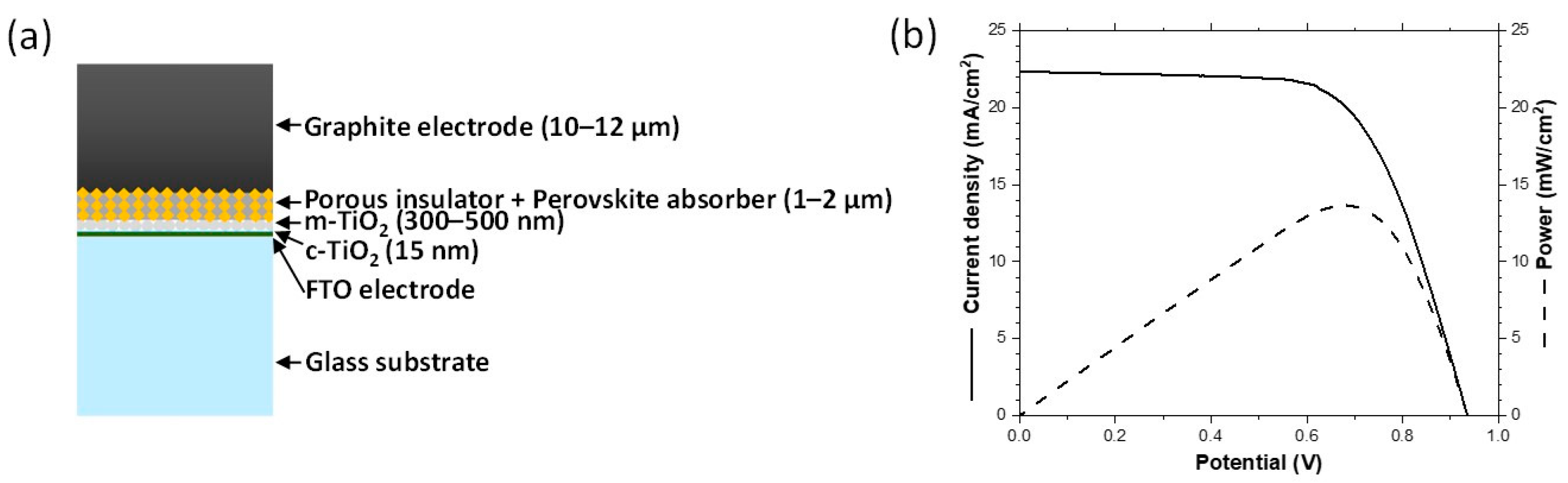
2.1. Fabrication of the c-PSC Devices
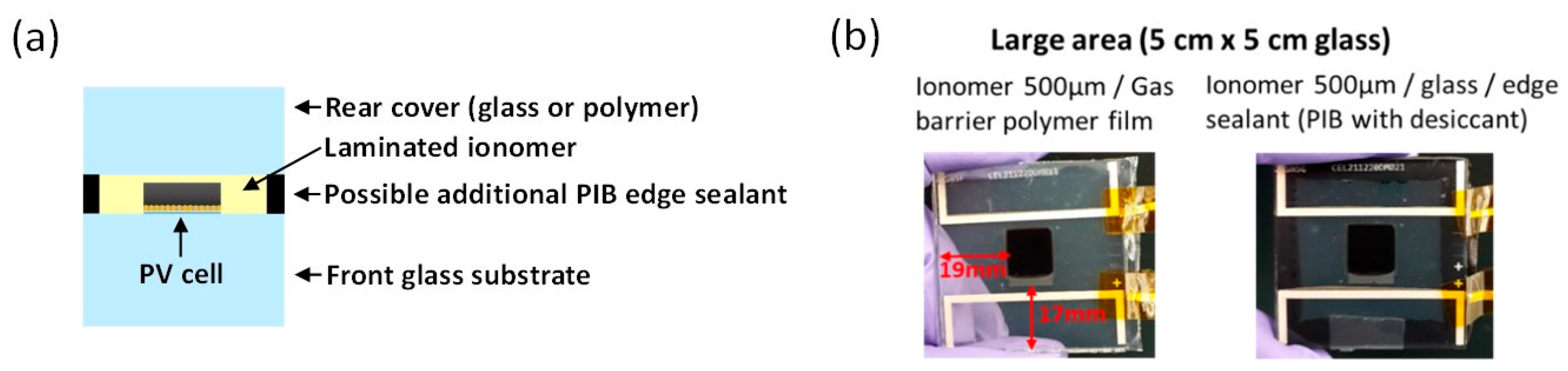
2.2. Encapsulation of the Photovoltaic Devices
2.3. Aging Campaigns
2.4. Characterizations
3. Results and Discussions
3.1. Impact of the Lamination Processes on c-PSC Devices
3.2. Aging of c-PSC Encapsulating Devices
3.2.1. Evolution of Photovoltaic Performances and Parameters
3.2.2. LBIC Mapping
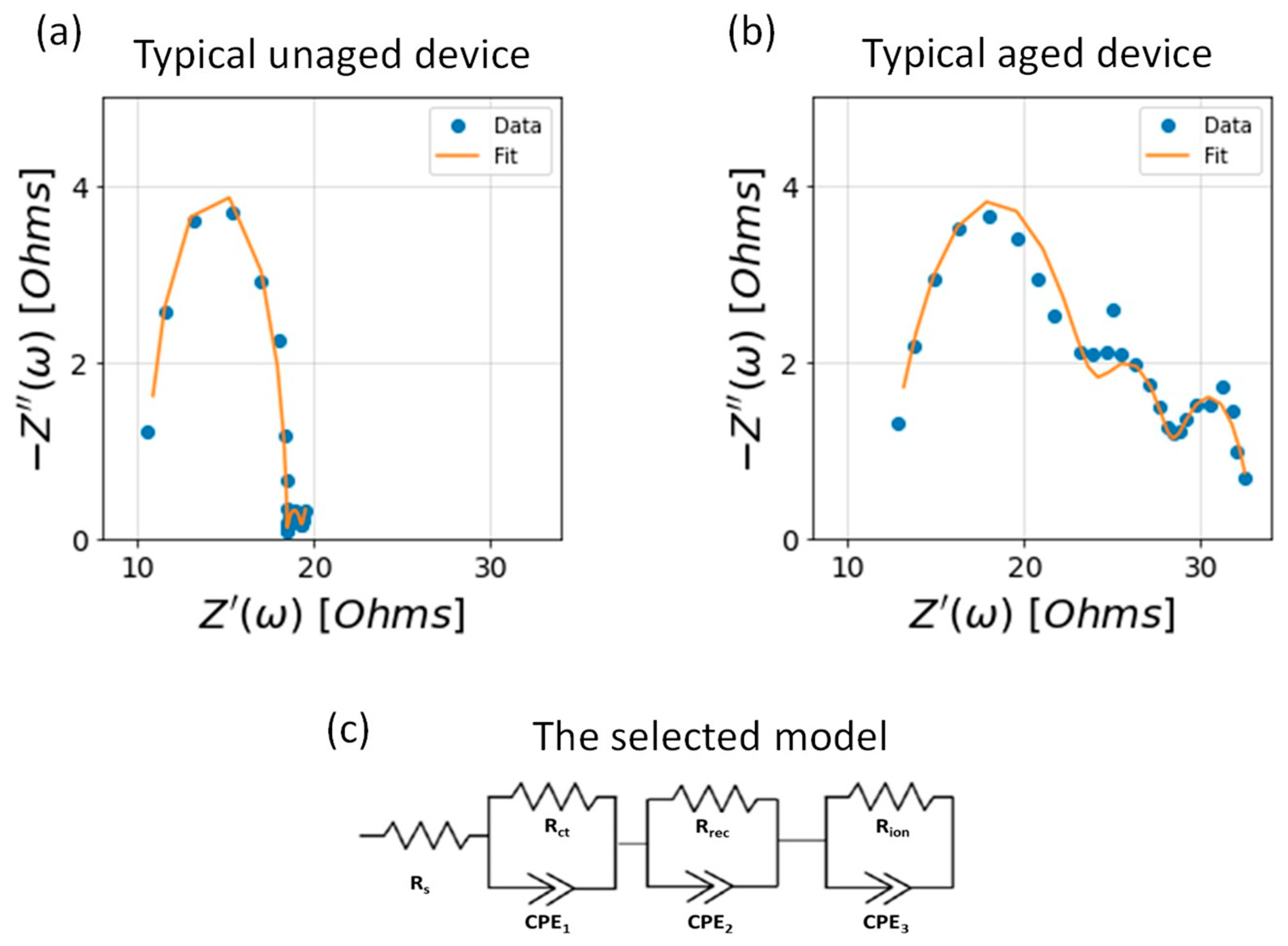
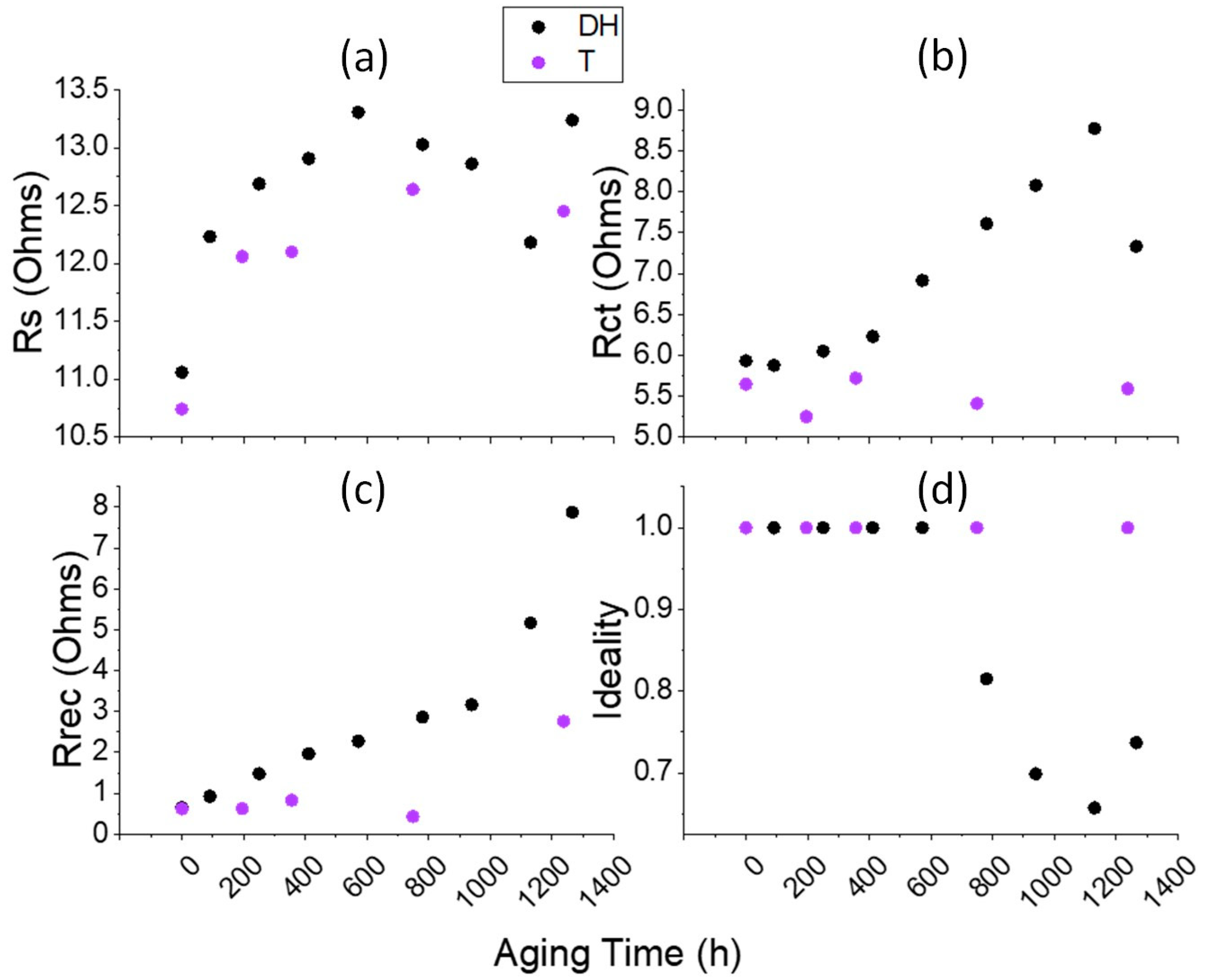
3.2.3. Impedance Spectroscopy
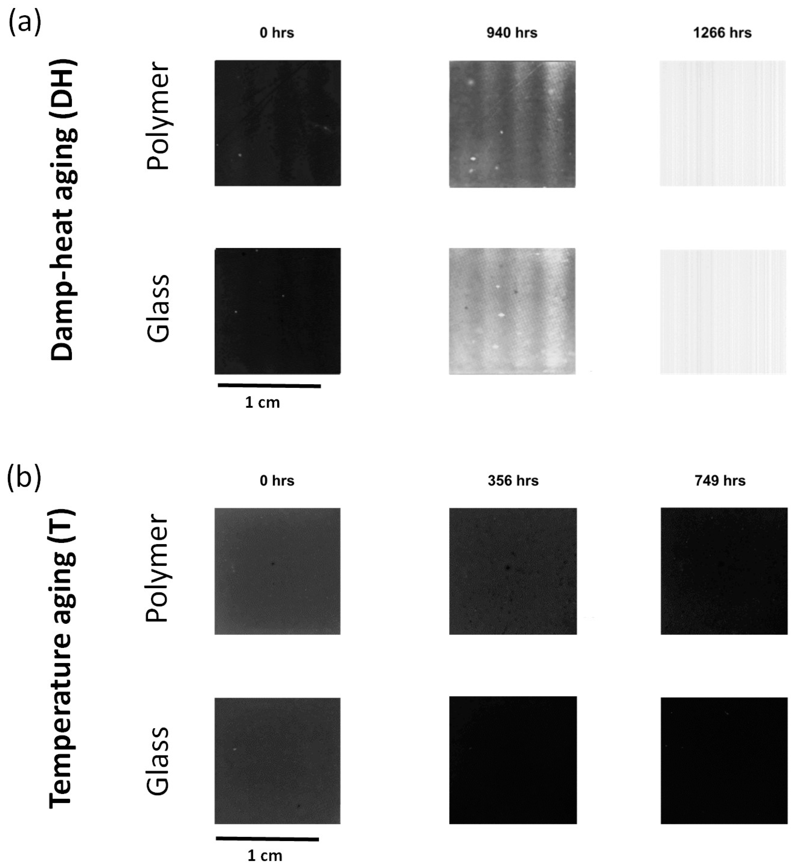
3.2.4. PL Imaging
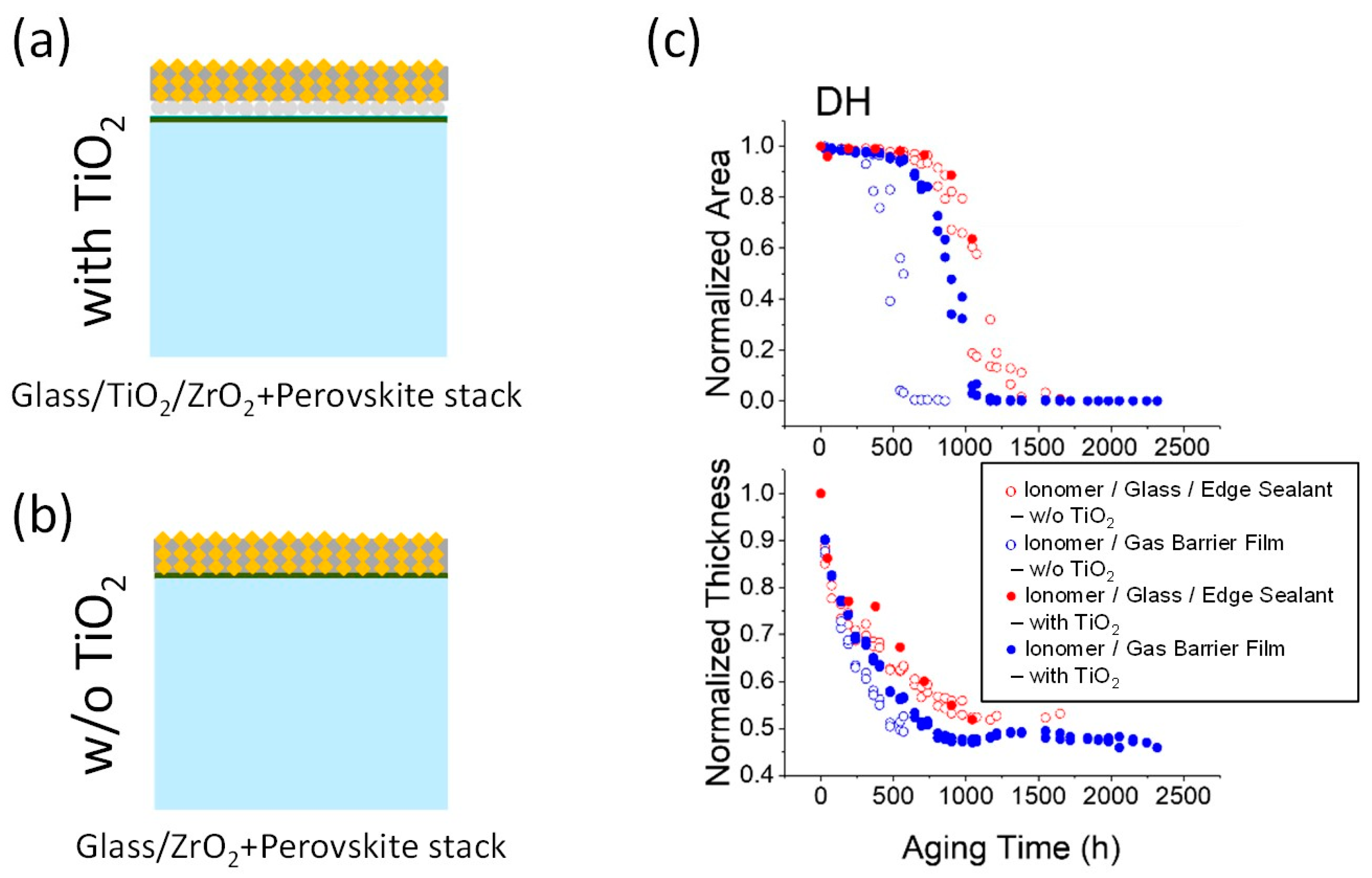
3.2.5. Area and Thickness Evolution of the Perovskite Layer
4. Conclusions
Supplementary Materials
Author Contributions
Funding
Data Availability Statement
Conflicts of Interest
References
- NREL. Best Research-Cell Efficiency Chart. Available online: https://www.nrel.gov/pv/cell-efficiency.html (accessed on 21 July 2023).
- Kim, H.-S.; Lee, C.-R.; Im, J.-H.; Lee, K.-B.; Moehl, T.; Marchioro, A.; Moon, S.-J.; Humphry-Baker, R.; Yum, J.-H.; Moser, J.E.; et al. Lead Iodide Perovskite Sensitized All-Solid-State Submicron Thin Film Mesoscopic Solar Cell with Efficiency Exceeding 9%. Sci. Rep. 2012, 2, 591. [Google Scholar] [CrossRef] [PubMed]
- Han, Y.; Meyer, S.; Dkhissi, Y.; Weber, K.; Pringle, J.M.; Bach, U.; Spiccia, L.; Cheng, Y.-B. Degradation Observations of Encapsulated Planar CH 3 NH 3 PbI 3 Perovskite Solar Cells at High Temperatures and Humidity. J. Mater. Chem. A 2015, 3, 8139–8147. [Google Scholar] [CrossRef]
- Burschka, J.; Pellet, N.; Moon, S.-J.; Humphry-Baker, R.; Gao, P.; Nazeeruddin, M.K.; Grätzel, M. Sequential Deposition as a Route to High-Performance Perovskite-Sensitized Solar Cells. Nature 2013, 499, 316–319. [Google Scholar] [CrossRef] [PubMed]
- Zheng, H.; Liu, G.; Zhang, C.; Zhu, L.; Alsaedi, A.; Hayat, T.; Pan, X.; Dai, S. The Influence of Perovskite Layer and Hole Transport Material on the Temperature Stability about Perovskite Solar Cells. Sol. Energy 2018, 159, 914–919. [Google Scholar] [CrossRef]
- Kobayashi, E.; Tsuji, R.; Martineau, D.; Hinsch, A.; Ito, S. Light-Induced Performance Increase of Carbon-Based Perovskite Solar Module for 20-Year Stability. Cell Rep. Phys. Sci. 2021, 2, 100648. [Google Scholar] [CrossRef]
- Emery, Q.; Remec, M.; Paramasivam, G.; Janke, S.; Dagar, J.; Ulbrich, C.; Schlatmann, R.; Stannowski, B.; Unger, E.; Khenkin, M. Encapsulation and Outdoor Testing of Perovskite Solar Cells: Comparing Industrially Relevant Process with a Simplified Lab Procedure. ACS Appl. Mater. Interfaces 2022, 14, 5159–5167. [Google Scholar] [CrossRef]
- Mei, A.; Li, X.; Liu, L.; Ku, Z.; Liu, T.; Rong, Y.; Xu, M.; Hu, M.; Chen, J.; Yang, Y.; et al. A Hole-Conductor-Free, Fully Printable Mesoscopic Perovskite Solar Cell with High Stability. Science 2014, 345, 295–298. [Google Scholar] [CrossRef]
- Fagiolari, L.; Bella, F. Carbon-Based Materials for Stable, Cheaper and Large-Scale Processable Perovskite Solar Cells. Energy Environ. Sci. 2019, 12, 3437–3472. [Google Scholar] [CrossRef]
- Zouhair, S.; Yoo, S.; Bogachuk, D.; Herterich, J.P.; Lim, J.; Kanda, H.; Son, B.; Yun, H.J.; Würfel, U.; Chahboun, A.; et al. Employing 2D-Perovskite as an Electron Blocking Layer in Highly Efficient (18.5%) Perovskite Solar Cells with Printable Low Temperature Carbon Electrode. Adv. Energy Mater. 2022, 12, 2200837. [Google Scholar] [CrossRef]
- Perrin, L.; Flandin, L.; Farha, C.; Narbey, S.; Martineau, D.; Planès, E. Investigation of Post-Treatment Improving Perovskite Solar Cells Initial Performances and Study of Its Impact on the Durability. Energies 2023, 16, 5254. [Google Scholar] [CrossRef]
- Bai, Y.; Mora-Seró, I.; De Angelis, F.; Bisquert, J.; Wang, P. Titanium Dioxide Nanomaterials for Photovoltaic Applications. Chem. Rev. 2014, 114, 10095–10130. [Google Scholar] [CrossRef]
- Gusmano, G.; Montesperelli, G.; Rapone, M.; Padeletti, G.; Cusmà, A.; Kaciulis, S.; Mezzi, A.; Maggio, R.D. Zirconia Primers for Corrosion Resistant Coatings. Surf. Coat. Technol. 2007, 201, 5822–5828. [Google Scholar] [CrossRef]
- Rao, M.K.; Sangeetha, D.N.; Selvakumar, M.; Sudhakar, Y.N.; Mahesha, M.G. Review on Persistent Challenges of Perovskite Solar Cells’ Stability. Sol. Energy 2021, 218, 469–491. [Google Scholar] [CrossRef]
- Pradid, P.; Sanglee, K.; Thongprong, N.; Chuangchote, S. Carbon Electrodes in Perovskite Photovoltaics. Materials 2021, 14, 5989. [Google Scholar] [CrossRef] [PubMed]
- Mei, A.; Sheng, Y.; Ming, Y.; Hu, Y.; Rong, Y.; Zhang, W.; Luo, S.; Na, G.; Tian, C.; Hou, X.; et al. Stabilizing Perovskite Solar Cells to IEC61215:2016 Standards with over 9000-h Operational Tracking. Joule 2020, 4, 2646–2660. [Google Scholar] [CrossRef]
- Huang, T.; Tan, S.; Yang, Y. Material, Phase, and Interface Stability of Photovoltaic Perovskite: A Perspective. J. Phys. Chem. C 2021, 125, 19088–19096. [Google Scholar] [CrossRef]
- Kundu, S.; Kelly, T.L. In Situ Studies of the Degradation Mechanisms of Perovskite Solar Cells. EcoMat 2020, 2, e12025. [Google Scholar] [CrossRef]
- Aitola, K.; Gava Sonai, G.; Markkanen, M.; Jaqueline Kaschuk, J.; Hou, X.; Miettunen, K.; Lund, P.D. Encapsulation of Commercial and Emerging Solar Cells with Focus on Perovskite Solar Cells. Sol. Energy 2022, 237, 264–283. [Google Scholar] [CrossRef]
- Fu, Z.; Xu, M.; Sheng, Y.; Yan, Z.; Meng, J.; Tong, C.; Li, D.; Wan, Z.; Ming, Y.; Mei, A.; et al. Encapsulation of Printable Mesoscopic Perovskite Solar Cells Enables High Temperature and Long-Term Outdoor Stability. Adv. Funct. Mater. 2019, 29, 1809129. [Google Scholar] [CrossRef]
- Shi, L.; Young, T.L.; Kim, J.; Sheng, Y.; Wang, L.; Chen, Y.; Feng, Z.; Keevers, M.J.; Hao, X.; Verlinden, P.J.; et al. Accelerated Lifetime Testing of Organic–Inorganic Perovskite Solar Cells Encapsulated by Polyisobutylene. ACS Appl. Mater. Interfaces 2017, 9, 25073–25081. [Google Scholar] [CrossRef]
- Cao, K.; Zuo, Z.; Cui, J.; Shen, Y.; Moehl, T.; Zakeeruddin, S.M.; Grätzel, M.; Wang, M. Efficient Screen Printed Perovskite Solar Cells Based on Mesoscopic TiO2/Al2O3/NiO/Carbon Architecture. Nano Energy 2015, 17, 171–179. [Google Scholar] [CrossRef]
- Martins, J.; Emami, S.; Madureira, R.; Mendes, J.; Ivanou, D.; Mendes, A. Novel Laser-Assisted Glass Frit Encapsulation for Long-Lifetime Perovskite Solar Cells. J. Mater. Chem. A 2020, 8, 20037–20046. [Google Scholar] [CrossRef]
- Luo, Q.; Ma, H.; Zhang, Y.; Yin, X.; Yao, Z.; Wang, N.; Li, J.; Fan, S.; Jiang, K.; Lin, H. Cross-Stacked Superaligned Carbon Nanotube Electrodes for Efficient Hole Conductor-Free Perovskite Solar Cells. J. Mater. Chem. A 2016, 4, 5569–5577. [Google Scholar] [CrossRef]
- Bella, F.; Griffini, G.; Correa-Baena, J.-P.; Saracco, G.; Gratzel, M.; Hagfeldt, A.; Turri, S.; Gerbaldi, C. Improving Efficiency and Stability of Perovskite Solar Cells with Photocurable Fluoropolymers. Science 2016, 354, 203–206. [Google Scholar] [CrossRef] [PubMed]
- Pescetelli, S.; Agresti, A.; Viskadouros, G.; Razza, S.; Rogdakis, K.; Kalogerakis, I.; Spiliarotis, E.; Leonardi, E.; Mariani, P.; Sorbello, L.; et al. Integration of Two-Dimensional Materials-Based Perovskite Solar Panels into a Stand-Alone Solar Farm. Nat. Energy 2022, 7, 597–607. [Google Scholar] [CrossRef]
- Li, J.; Xia, R.; Qi, W.; Zhou, X.; Cheng, J.; Chen, Y.; Hou, G.; Ding, Y.; Li, Y.; Zhao, Y.; et al. Encapsulation of Perovskite Solar Cells for Enhanced Stability: Structures, Materials and Characterization. J. Power Sources 2021, 485, 229313. [Google Scholar] [CrossRef]
- Wang, Y.; Ahmad, I.; Leung, T.; Lin, J.; Chen, W.; Liu, F.; Ng, A.M.C.; Zhang, Y.; Djurišić, A.B. Encapsulation and Stability Testing of Perovskite Solar Cells for Real Life Applications. ACS Mater. Au 2022, 2, 215–236. [Google Scholar] [CrossRef] [PubMed]
- Tracy, J.; Bosco, N.; Delgado, C.; Dauskardt, R. Durability of Ionomer Encapsulants in Photovoltaic Modules. Sol. Energy Mater. Sol. Cells 2020, 208, 110397. [Google Scholar] [CrossRef]
- Wiesmeier, C.; Headrich, I.; Weiss, K.-A.; Duerr, I. Overview of PV Module Encapsulation Materials. Photovolt. Int. 2013, 19, 85–92. [Google Scholar]
- Zhang, Y.; Xu, J.; Mao, J.; Tao, J.; Shen, H.; Chen, Y.; Feng, Z.; Verlinden, P.J.; Yang, P.; Chu, J. Long-Term Reliability of Silicon Wafer-Based Traditional Backsheet Modules and Double Glass Modules. RSC Adv. 2015, 5, 65768–65774. [Google Scholar] [CrossRef]
- Slauch, I.M.; Vishwakarma, S.; Tracy, J.; Gambogi, W.; Meier, R.; Rahman, F.; Hartley, J.Y.; Bertoni, M.I. Manufacturing Induced Bending Stresses: Glass-Glass vs. Glass-Backsheet. In Proceedings of the 2021 IEEE 48th Photovoltaic Specialists Conference (PVSC), IEEE, Fort Lauderdale, FL, USA, 20 June 2021; pp. 1943–1948. [Google Scholar]
- Singh, J.P.; Guo, S.; Peters, I.M.; Aberle, A.G.; Walsh, T.M. Comparison of Glass/Glass and Glass/Backsheet PV Modules Using Bifacial Silicon Solar Cells. IEEE J. Photovolt. 2015, 5, 783–791. [Google Scholar] [CrossRef]
- Stefanelli, M.; Vesce, L.; Di Carlo, A. Upscaling of Carbon-Based Perovskite Solar Module. Nanomaterials 2023, 13, 313. [Google Scholar] [CrossRef] [PubMed]
- Abdulrahim, S.M.; Ahmad, Z.; Bahadra, J.; Al-Thani, N.J. Electrochemical Impedance Spectroscopy Analysis of Hole Transporting Material Free Mesoporous and Planar Perovskite Solar Cells. Nanomaterials 2020, 10, 1635. [Google Scholar] [CrossRef]
- von Hauff, E. Impedance Spectroscopy for Emerging Photovoltaics. J. Phys. Chem. C 2019, 123, 11329–11346. [Google Scholar] [CrossRef]
- Getting Started with Impedance.Py. Available online: https://impedancepy.readthedocs.io/en/latest/getting-started.html (accessed on 21 July 2023).
- PyPI Pillow 9.1.0. Available online: https://pypi.org/project/Pillow (accessed on 21 July 2023).
- Booker, E.; Boutin, J.-B.; Roux, C.; Manceau, M.; Berson, S.; Cros, S. Perovskite Test: A High Throughput Method to Screen Ambient Encapsulation Conditions. Energy Technol. 2020, 8, 2000041. [Google Scholar] [CrossRef]
- Taherimakhsousi, N.; Fievez, M.; MacLeod, B.P.; Booker, E.P.; Fayard, E.; Matheron, M.; Manceau, M.; Cros, S.; Berson, S.; Berlinguette, C.P. A Machine Vision Tool for Facilitating the Optimization of Large-Area Perovskite Photovoltaics. NPJ Comput. Mater. 2021, 7, 190. [Google Scholar] [CrossRef]
- Lange, R.F.M.; Luo, Y.; Polo, R.; Zahnd, J. The Lamination of (Multi)Crystalline and Thin Film Based Photovoltaic Modules. Prog. Photovolt. Res. Appl. 2011, 19, 127–133. [Google Scholar] [CrossRef]
- Ramasamy, E.; Karthikeyan, V.; Rameshkumar, K.; Veerappan, G. Glass-to-Glass Encapsulation with Ultraviolet Light Curable Epoxy Edge Sealing for Stable Perovskite Solar Cells. Mater. Lett. 2019, 250, 51–54. [Google Scholar] [CrossRef]
- Kempe, M.D.; Nobles, D.L.; Postak, L.; Calderon, J.A. Moisture Ingress Prediction in Polyisobutylene-based Edge Seal with Molecular Sieve Desiccant. Prog. Photovolt. Res. Appl. 2018, 26, 93–101. [Google Scholar] [CrossRef]
- Chen, Y.; Meng, Q.; Xiao, Y.; Zhang, X.; Sun, J.; Han, C.B.; Gao, H.; Zhang, Y.; Lu, Y.; Yan, H. Mechanism of PbI2 in Situ Passivated Perovskite Films for Enhancing the Performance of Perovskite Solar Cells. ACS Appl. Mater. Interfaces 2019, 11, 44101–44108. [Google Scholar] [CrossRef]
- Boyd, C.C.; Cheacharoen, R.; Leijtens, T.; McGehee, M.D. Understanding Degradation Mechanisms and Improving Stability of Perovskite Photovoltaics. Chem. Rev. 2019, 119, 3418–3451. [Google Scholar] [CrossRef]
- Goetz, K.P.; Taylor, A.D.; Paulus, F.; Vaynzof, Y. Shining Light on the Photoluminescence Properties of Metal Halide Perovskites. Adv. Funct. Mater. 2020, 30, 1910004. [Google Scholar] [CrossRef]
- Wagner, L.; Mundt, L.E.; Mathiazhagan, G.; Mundus, M.; Schubert, M.C.; Mastroianni, S.; Würfel, U.; Hinsch, A.; Glunz, S.W. Distinguishing Crystallization Stages and Their Influence on Quantum Efficiency during Perovskite Solar Cell Formation in Real-Time. Sci. Rep. 2017, 7, 14899. [Google Scholar] [CrossRef]
- Tian, T.; Zhong, J.; Yang, M.; Feng, W.; Zhang, C.; Zhang, W.; Abdi, Y.; Wang, L.; Lei, B.; Wu, W. Interfacial Linkage and Carbon Encapsulation Enable Full Solution-Printed Perovskite Photovoltaics with Prolonged Lifespan. Angew. Chem. Int. Ed. 2021, 60, 23735–23742. [Google Scholar] [CrossRef] [PubMed]
- Choi, J.-M.; Suko, H.; Kim, K.; Han, J.; Lee, S.; Matsuo, Y.; Maruyama, S.; Jeon, I.; Daiguji, H. Multi-Walled Carbon Nanotube-Assisted Encapsulation Approach for Stable Perovskite Solar Cells. Molecules 2021, 26, 5060. [Google Scholar] [CrossRef] [PubMed]
- Runser, R.; Kodur, M.; Skaggs, J.H.; Cakan, D.N.; Foley, J.B.; Finn, M.; Fenning, D.P.; Lipomi, D.J. Stability of Perovskite Films Encapsulated in Single- and Multi-Layer Graphene Barriers. ACS Appl. Energy Mater. 2021, 4, 10314–10322. [Google Scholar] [CrossRef]
- IEC 61215-1:2021; Terrestrial Photovoltaic (PV) Modules—Design Qualification and Type Approval. IEC Webstore: Geneva, Switzerland, 2021. Available online: https://webstore.iec.ch/publication/61345 (accessed on 10 September 2023).


| 18 Cells Batch | PCE (%) | Jsc (mA/cm2) | Voc (V) | FF |
|---|---|---|---|---|
| Average value | 13.26 | 22.60 | 0.927 | 0.63 |
| Standard deviation | ±0.64 | ±0.59 | ±0.007 | ±0.02 |
| PCE (%) | Jsc (mA/cm2) | Voc (V) | FF | |
|---|---|---|---|---|
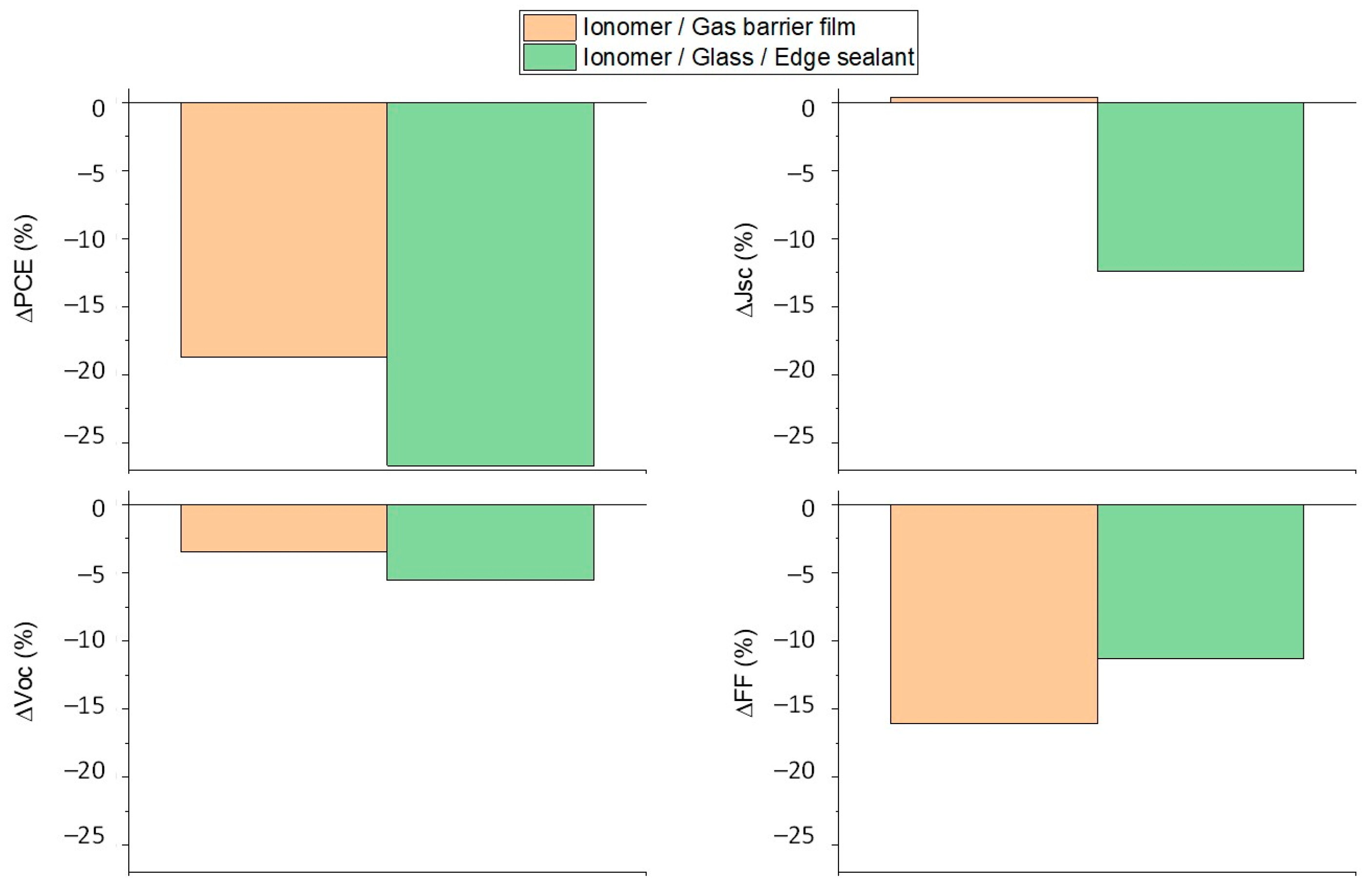
| Ionomer/Gas barrier film DH 2200 h | 1.73 | 4.01 | 0.885 | 0.49 |
| Standard Deviation | ±0.13 | ±0.15 | ±0.015 | ±0.03 |
| Ionomer/Glass/Edge sealant DH 2200 h | 0.44 | 1.23 | 0.753 | 0.41 |
| Standard Deviation | ±0.31 | ±0.69 | ±0.079 | ±0.06 |
| Ionomer/Gas barrier film T 2600 h | 7.36 | 19.63 | 0.915 | 0.41 |
| Standard Deviation | ±0.13 | ±0.11 | ±0.008 | ±0.01 |
| Ionomer/Glass/Edge sealant T 2600 h | 6.41 | 15.03 | 0.931 | 0.47 |
| Standard Deviation | ±1.88 | ±5.19 | ±0.006 | ±0.02 |
Disclaimer/Publisher’s Note: The statements, opinions and data contained in all publications are solely those of the individual author(s) and contributor(s) and not of MDPI and/or the editor(s). MDPI and/or the editor(s) disclaim responsibility for any injury to people or property resulting from any ideas, methods, instructions or products referred to in the content. |
© 2023 by the authors. Licensee MDPI, Basel, Switzerland. This article is an open access article distributed under the terms and conditions of the Creative Commons Attribution (CC BY) license (https://creativecommons.org/licenses/by/4.0/).
Share and Cite
Kyranaki, N.; Perrin, L.; Flandin, L.; Planès, E.; Farha, C.; Wagner, L.; Saddedine, K.; Martineau, D.; Cros, S. Comparison of Glass–Glass versus Glass–Backsheet Encapsulation Applied to Carbon-Based Perovskite Solar Cells. Processes 2023, 11, 2742. https://doi.org/10.3390/pr11092742
Kyranaki N, Perrin L, Flandin L, Planès E, Farha C, Wagner L, Saddedine K, Martineau D, Cros S. Comparison of Glass–Glass versus Glass–Backsheet Encapsulation Applied to Carbon-Based Perovskite Solar Cells. Processes. 2023; 11(9):2742. https://doi.org/10.3390/pr11092742
Chicago/Turabian StyleKyranaki, Nikoleta, Lara Perrin, Lionel Flandin, Emilie Planès, Cynthia Farha, Lukas Wagner, Karima Saddedine, David Martineau, and Stéphane Cros. 2023. "Comparison of Glass–Glass versus Glass–Backsheet Encapsulation Applied to Carbon-Based Perovskite Solar Cells" Processes 11, no. 9: 2742. https://doi.org/10.3390/pr11092742
APA StyleKyranaki, N., Perrin, L., Flandin, L., Planès, E., Farha, C., Wagner, L., Saddedine, K., Martineau, D., & Cros, S. (2023). Comparison of Glass–Glass versus Glass–Backsheet Encapsulation Applied to Carbon-Based Perovskite Solar Cells. Processes, 11(9), 2742. https://doi.org/10.3390/pr11092742