1. Introduction
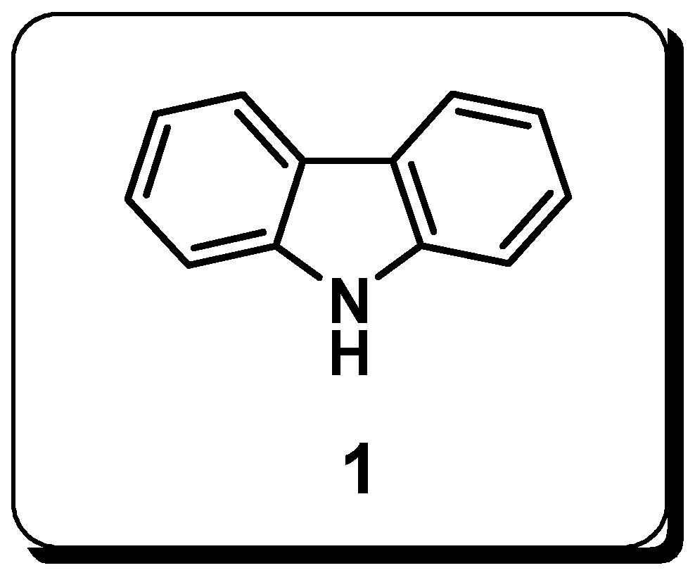
9H-Carbazole (1), often referred to as carbazole, shown in
Figure 1, is a tricyclic molecule that can be obtained from natural sources. It was first obtained from the anthracene fraction of distilled coal tar.
Carbazole has an aromatic system with extensive electron delocalization. The structure of the compound is based on the indole structure, in which a second benzene ring is fused to the five-membered ring at the 2–3 position of the indole or a pyrrole ring is fused to two benzene rings, both of which lead to the same final structure. The presence of pyrrole increases the electron-rich nature of carbazole, and its full aromaticity provides it with the property of hole transport. When excited, the lone pair of electrons of nitrogen occupies the lowest unoccupied molecular orbital (LUMO), generating a hole in the highest occupied molecular orbital (HOMO) that moves through the structure. Owing to the nitrogen of the pyrrole ring, carbazoles can be easily functionalized, generating a range of materials with diverse applications [
1]. However, the main properties discussed in this work are those of optoelectronic devices such as solar cells and light-emitting diodes. Carbazole is a molecular scaffold that offers advantages such as good hole transport, high thermal and electrochemical stability, high photoluminescence quantum yield (PLQY), and ease of functionalization at different sites [
2]. These characteristics impart attractive optical and electronic properties. Structural modification strategies have been applied to carbazole-based compounds to optimize their emission efficiency, triplet energy, and thermal stability. The advantages associated with carbazoles can be contrasted with the most efficient counterparts, which are metal-based dyes. While these compounds have lab-scale PCE (power conversion efficiency) up to 14.3%, there are several limitations since the most active ones are Ru-based complexes sensitizers, which suffer from issues related to high costs and toxicity, as well as poor stability to endure several years of turnover. In the case of quantum dots (QDs), many types of QDs, such as CdS, CdTe, or core–shell semiconducting nanocrystals (CdS/HgS, CdS/CdSe, and ZnSe/CdSe) have been explored within this class. Apart from the good extinction coefficients, the environmental concerns associated with the high percentage of heavy metals in its composition also represent an obstacle and a preventive factor for cost-effective and environment-friendly DSSC systems. Thus, metal-free systems can be versatile and cheap, demonstrating a huge potential to increase efficiency by tailoring electrochemical and optical properties [
3].
This mini-review aims to provide a brief overview of the fundamentals of OLEDs and solar cells, focusing on the use of carbazole derivatives and their applications in these devices. Firstly, the basics of solar cells, highlighting the main efficiency parameters, are presented. There have been several reported applications of carbazole polymers in organic electronics, and
Section 2 highlights recent developments through selected examples of the use of the molecular approach in third-generation dye-sensitized and perovskite solar cells. In the following section, the development of OLEDs in the context of carbazoles illustrates the versatility of these compounds, which have opened new frontiers in designing unique functional materials. To conclude this mini-review, we reinforce some characteristics of these compounds for advancing novel and efficient devices.
3. Photovoltaic Parameters
Photovoltaic cells assume the photovoltaic effect that occurs in a p–n junction of doped semiconductors, with the consequent passage of current through an external circuit from the illumination of this junction.
The specifications of the photovoltaic cell were obtained through well-standardized tests in various studies on the subject. The operating conditions in which the cells are subjected to the tests are lighting with a spectrum called Air Mass 1.5 G, which corresponds to the spectrum of sunlight when it is at an angle of 42° and the standardization of the power of the light source at 1000 W/m
2 or 100 mW/cm
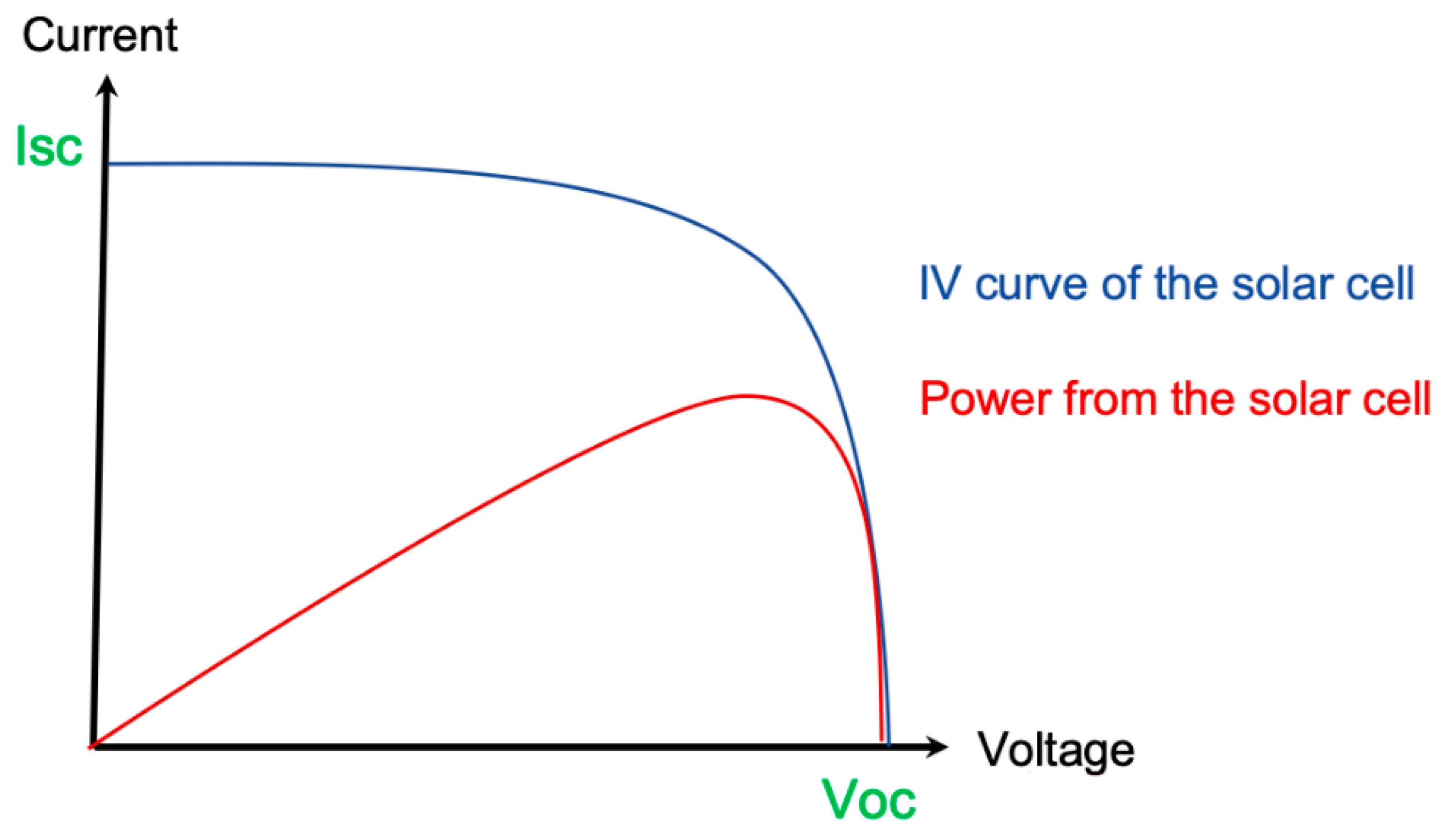
2. The cell was connected to a potentiostat to obtain the photovoltaic parameters. Linear voltammetry was performed under illumination. This technique involves varying the potential (V) while measuring current (I). This produces a voltammogram, which, in this type of study, is called the current versus potential curve (I × V), as shown in
Figure 3. Using the I × V curve, it is possible to obtain parameters such as the open circuit voltage or potential (V
oc, oc for open circuit), which is the maximum voltage value for a solar cell and occurs when the current passing the device is zero and the short circuit current (I
sc, sc for short circuit), that is the maximum current from a solar cell and occurs when the voltage across the device is zero. When the cell was illuminated, a current was produced. When the potential applied by the potentiostat was equal to zero, the device was in a short circuit condition. At this point, it presents the highest current under the operating conditions. When the potential is varied, a condition is reached in which the intrinsic potential of the cell is equal to that applied by the potentiostat, ceasing the flow of the current in the device. At this point, we have open circuit potential.
Cell power was obtained by multiplying the current and voltage parameters. The device power curve displays the maximum power (Pmax), at which point we have a corresponding voltage value (Vpmax) associated, and comparing this value to the I × V curve, we have the current value (Ipmax) that corresponds to the maximum power. It is common to normalize the current generated by a cell by dividing its value by the area of the device, thus obtaining the current density (J). This is because devices with larger areas lead to greater current generation, which would make it difficult to compare the two different devices. Therefore, the current density is usually used in calculations instead of the current generation. With the values of Jsc, Voc, Pmax, Vpmax, and Jpmax, it is possible to determine the performance of the solar cell through the efficiency (η) and fill factor (FF). The fill factor is the ratio of the powers that shows the relationship between the maximum power obtained and the maximum possible power. It is obtained by dividing the maximum power displayed by the device by the multiple of Jsc and Voc, which is also power.
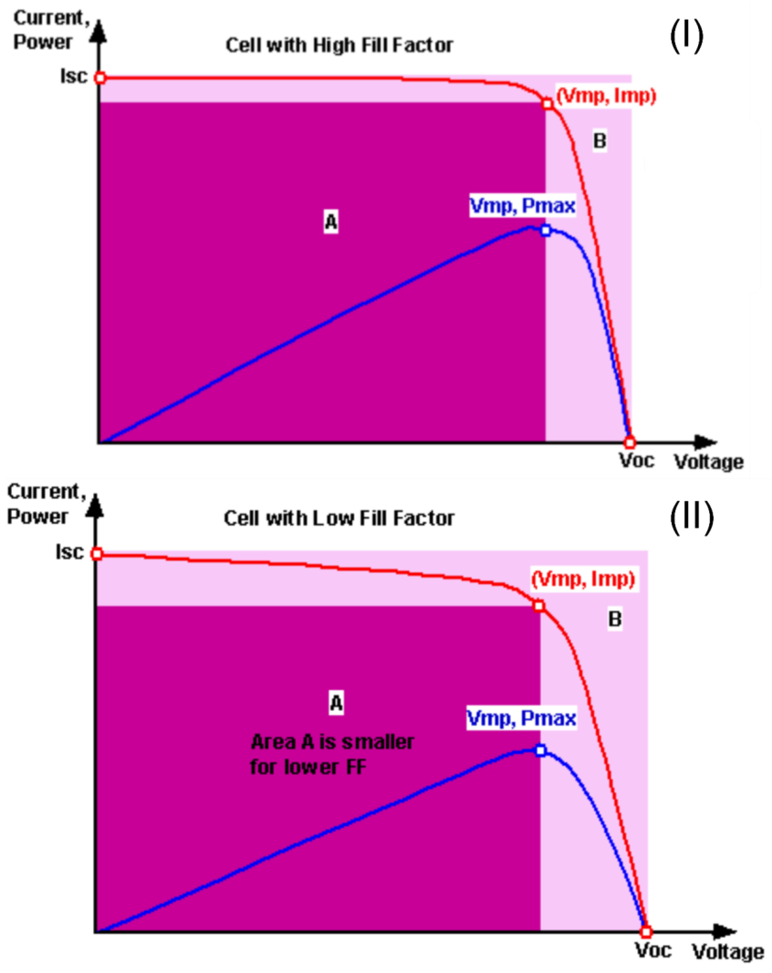
The maximum possible value that the fill factor could display is 1 (or 100%). The fill factor can also be interpreted graphically as the ratio between the areas. In the I × V graph (I) in
Figure 4, the fill factor is the ratio between areas A and B. In curve (II), the cell performance was lower than before, so the curve loses part of its characteristic shape, and consequently, area A is smaller, leading to a lower fill factor.
The efficiency (η) is a parameter that measures the efficiency of a device’s conversion of solar energy into electrical energy. It is the main parameter to be compared between the two different devices in this area of study.
4. Types of Solar Cells
Devices based on amorphous, polycrystalline, or monocrystalline semiconductor silicon have efficiencies between 5% and 15% [
9]. However, the disadvantages associated with this type of device are the high research cost associated with the relatively low conversion yield (below 30%) [
9] and the need to use high-purity semiconductor materials. According to Tiwari et al. [
10] and Hagfeldt et al. [
11], solar cells can be divided into three generations based on the type of technology used in their production.
First Generation: Consists of devices based on silicon with high purity (99.9999%), with a single p–n junction, presenting a large area, and involving processes that demand a lot of energy, making it difficult to reduce production costs.
Second Generation: These are based on the use of thin films using materials such as amorphous and microporous silicon and cadmium telluride (CdTe), which are the most promising. This generation also uses different production techniques, such as electrochemical and vapor deposition, to reduce costs.
Third generation: Large-scale energy production by increasing the efficiency of photovoltaic devices, especially those of the second generation, using cheaper materials and techniques to reduce the cost of the device. This definition also includes the combination of technologies and devices that surpass Shockley–Queisser’s limit (the maximum theoretical density of a solar cell in which the only loss is radiative recombination) [
12].
5. Dye-Sensitized Solar Cells Employing Carbazoles
Regarding third-generation cells, in 1991, Grätzel et al. [
13] proposed a dye-sensitized solar cell (DSSC) using relatively inexpensive materials, such as TiO
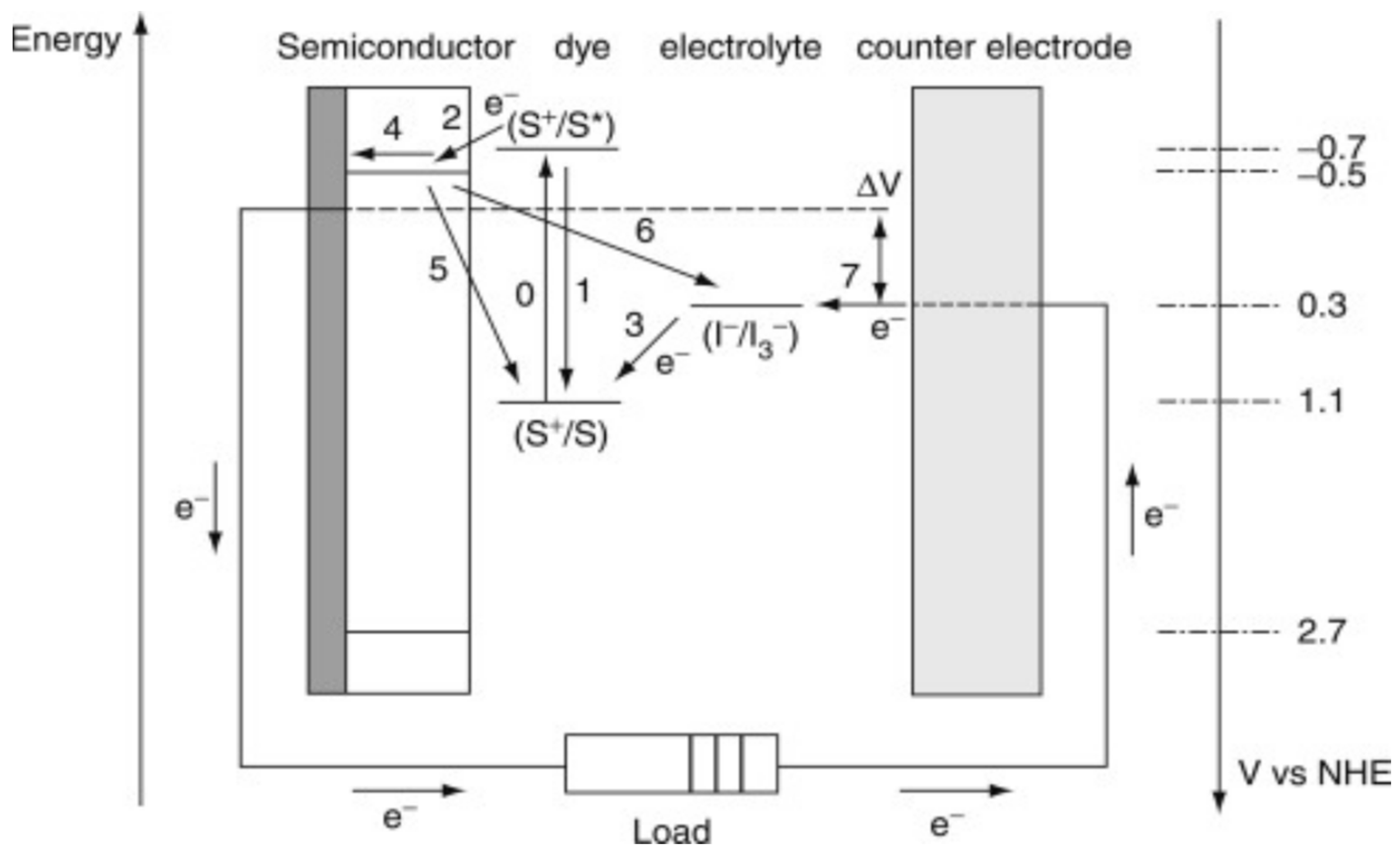
2 as the photoanode. This device is known as a dye-sensitized solar cell or a Grätzel cell. The operating mode is illustrated in
Figure 5. In general, the operation of the Grätzel cell involves the absorption of a photon by a dye molecule (D), leading to the excitation of an electron between the HOMO and LUMO of D, with subsequent injection of this electron into the conduction band (BC) of TiO
2 (the anode). The electron injected into the conduction band migrates to an external circuit, which is connected to the counter electrode. The dye then interacts with the electrolyte, which is originally based on an I
−/ I
3− solution, and its electrons are restored. Simultaneously, the generated iodine is reduced to iodide at the counter electrode (cathode) by the electrons that travel through the external circuit. Thus, the device generates electrical energy without undergoing permanent chemical transformation. The efficiency of conversion of artificial sunlight (AM 1.5 G) into electrical energy for the Grätzel cell is 11% on a laboratory scale (<1 cm
2 active area) and 8% for modules with larger areas (25–100 cm
2) [
14].
The presence of impurities in the crystal lattice of semiconductors can cause an excess of electrons or holes, increasing or reducing the conductivity of the semiconductor. DSSCs increase the conductivity of the semiconductor by transferring electrons to its conduction band (BC) without generating holes in the valence band (VB); the hole remains in the HOMO and LUMO orbitals of the dye. Therefore, the impregnation of an organic dye into the structure of the semiconductor of a solar cell (such as TiO
2) is essential because it needs to be in intimate contact. When excited, the electrons in the higher energy-filled molecular orbitals (HOMO) move to the conduction band of the semiconductor; that is, they become conduction electrons [
15].
The classical sensitizing dye is the cis-bis(isothiocyanate)-bis(2,2′bipyridyl-4,4′-dicarboxylate)-ruthenium (II) complex, represented by the code “N719”. However, this complex has a high acquisition cost, mainly because Ru is used as a metal core. In an attempt to reduce the operational cost, recent approaches have also been directed toward metal-free organic dyes because of the possibility of modulating the molar absorption coefficient through specific structural modifications [
16]. Many of these dyes have a structure that follows a donor-π spacer-acceptor (D-π-A) architecture [
17]. Carboxylic and cyanoacrylic acids [
18] and rhodamines [
19] are cores frequently added to D-π-A systems as electronic acceptors; donors and acceptors are interconnected by spacers such as polyenes, oligophenylenevinylenes, and oligothiophenes [
20]; coumarins [
21], indolines [
22], triphenylamines [
23], tetrahydroquinolines [
24], and carbazoles [
25] are used as electron donor units with good performance.
With regard to carbazole in sensitizing dyes, Elmorsy et al. [
25] reported the joint use of triphenylamine and N-substituted carbazole as donor units of D-π-A systems varying the acceptor unit from cyanoacrilic to carboxylic, nitrite and dicyanide motifs. Cell efficiency (
η) ranged from 6.51% to 8.89%, with the best result related to the employment of cyanoacrilic acid acceptor, while the fill factor (
FF) values ranged from 0.54 to 0.67. Again, the best result was associated with the presence of cyanoacrilic moiety in the structure. The authors affirmed that this sensitizing dye had the smallest HOMO–LUMO energy difference, which is related to decreased hardness, and hence to facilitated charge transfer. It is important to note that the results for the best performance dye overcame the classical N719 dye (
η = 7.60%;
FF = 0.56).
Naik et al. [
26] described the use of some donor structures containing carbazoles in different structural designs, such as D-π-A, D-D-π-A, and A-π-D-π-A with the same cyanoacetic acid as the acceptor unit. The main result is that the di-anchoring of the A-π-D-π-A architecture afforded superior cell VOC while the D-D-π-A structure with electron-releasing anisole as an auxiliary donor exhibited better
JSC; in contrast, all tested architectures gave an efficiency of 3.7%.
Derince et al. [
27] suggested the use of N-substituted carbazole as the donor unit and -CF3 moiety as the acceptor and anchoring unit in a ZnO-based DSSC. The efficiency values ranged from 0.004% to 0.025% and
FF from 0.36 to 0.42. No remarkable results were obtained; therefore, it is difficult to assign a cause for the cell’s underperformance. It would be necessary to know the role of CF3 units in attachment and charge transfer to the semiconductor layer, as well as to employ TiO
2 instead of ZnO in one experiment to detect any improvements the use of carbazoles with CF3 units brought to the classical DSSC.
Badu, Naik, and Keremone [
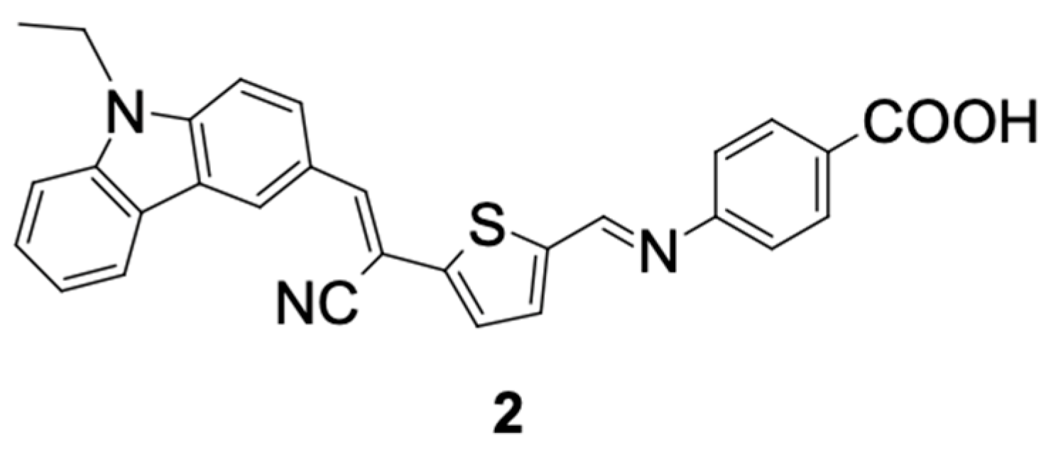
28] designed a new sensitizing dye called DP-1 (2), as shown in
Figure 6, for use in the construction of DSSCs. DP-1 (2) contains N-ethylcarbazole as a donor group, thiophene as a spacer group, and an acceptor group formed from 4-aminobenzoic acid. They reported that the presence of an ethyl group in the carbazole core reduces the aggregation state of the dye and unwanted recombination of the electrolyte. In addition, they suggested that π-conjugated bridges are essential for the stability of dyes.
Using the electronic absorption spectrum in the range of 300–550 nm, with a maximum peak at 431 nm, the sensitizing dye DP-1 (2) showed a 2.60% conversion efficiency (η), with a short circuit current (Jsc) of 5.95 mA.cm−2 and an open circuit current (Voc) of 0.59 V.
Neshile et al. [
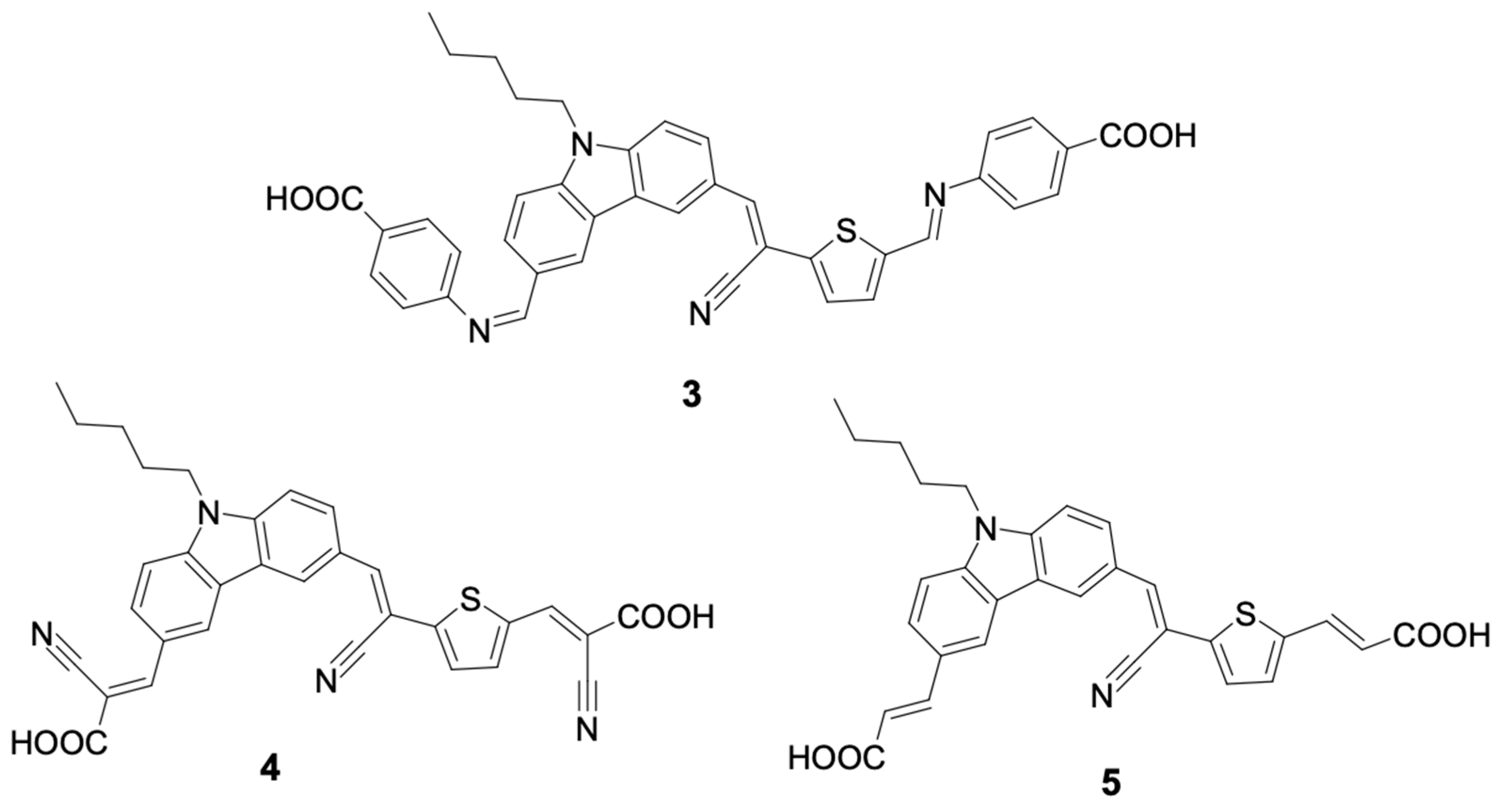
29] designed three new sensitizing dyes containing two electron acceptor groups and one electron donor group. Because of these two acceptor units, the approach was called di-anchoring, and the sensitizing dyes were named Car-Amin (
3), Car-Cy (
4), and Car-Mal (
5).
Figure 7 shows the structures of these dyes.
In the structures Car-Amin (3), Car-Cy (4), and Car-Mal (5), the donor unit is N-pentylcarbazole, which is a π-conjugated fragment formed by the cyano, vinylene, and thiophene groups, and the acceptor unit, which is derived from 2-cyanoacetic (Car-Cy, 4), 4-aminobenzoic (Car-Amin, 3), and malonic (Car-Mal, 5) acids. The Car-Amin dye (3) showed better energy conversion efficiency (PCE) under standard solar conditions, with a short circuit current (Jsc) of 2.27 mA.cm−2 and an open circuit current (Voc) of 0.54 V.
Kusumawati and Pamungkas [
30] constructed, from the carbazole core, two new sensitizing dyes capable of di-anchoring, named CBC0 (
6) and CBP1 (
7). In the structure of CBP0 (
6), the acceptor units are the two carboxyl groups. The replacement of the carboxyl group with a phosphonic group gives rise to the structure of CBP1 (
7). In the structures of CBP0 (
6) and CBP1 (
7), as shown in
Figure 8, the atom connected to the carbazole core was hydrogen.
The authors do not provide data on conversion efficiency (
η) and short circuit current (
Jsc) for the structures of CBP0 (
6) and CBP1 (
7). However, they provide information on open circuit current (
Voc) for both 2.741 V for CBP0 (
6) and 2.763 V for CBP1 (
7). The replacement of the carboxyl group by the phosphonic group proposed by the authors aims to investigate the effect on the electronic properties of these structures. Furthermore, in order to improve the electronic properties of the dye CBP1 (
7), the authors functionalized the nitrogen atom present in the structure of 9H-carbazole (
1) with ten different electron-donating groups, as shown in
Figure 9.
As previously mentioned, the authors do not show the conversion efficiency (η) and short circuit current (Jsc) data for the dyes derived from CBP1 (7). However, they once again describe the open circuit current data, which are in the range between 2.734 V and 2.766 V.
6. Perovskite Solar Cells Employing Carbazoles
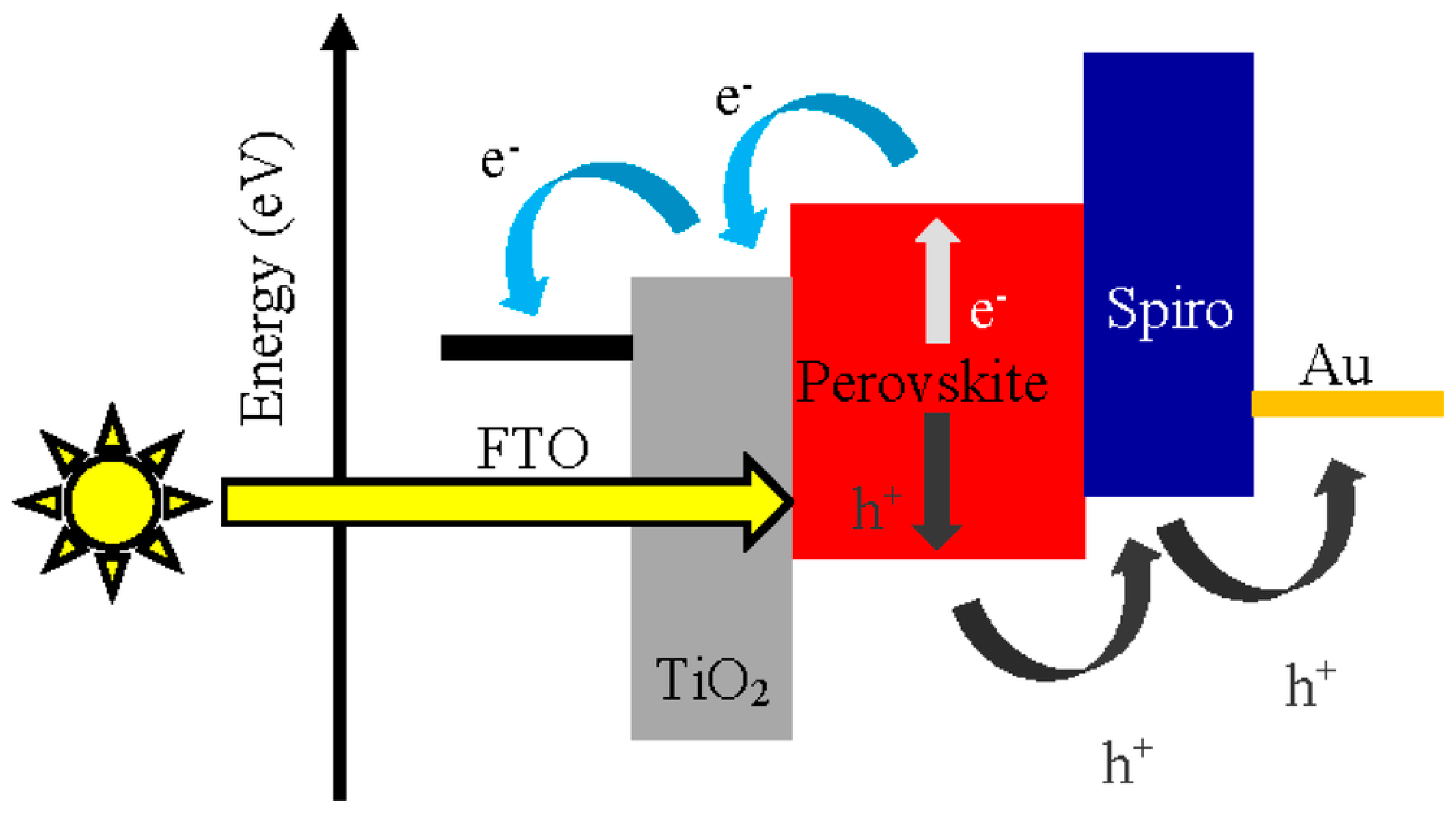
Perovskite solar cells (PSCs,
Figure 10) stand out among third-generation cells, having a similar operation to those that use sensitizing dyes, with the following basic structure: FTO/ETL/perovskite/HTL/Metal, with TiO
2 as the electron carrier (ETL) and SPIRO-OMeTAD (2,2′,7,7′-tetrakis[N,N-di(4-methoxyphenyl)amino]-9,9′-spirobifluorene) as the most common hole transport layer (HTL) (
Figure 10). However, its production cost, due to the complex synthesis of SPIRO-OMeTAD, and its efficiency (10%) are factors that limit its dissemination [
31]. However, this HTL has high charge recombination at the TiO
2/OMeTAD interface when there are holes present in the perovskite structure.
Currently, materials based on small organic molecules, such as carbazoles, have demonstrated better photovoltaic activities, easy functionalization, and simplified synthesis. Furthermore, studies reveal that perovskite solar cells that use this core as HTL have a good interface between their components, which is essential for the cell to function since the hole transporter needs not only to have an energy level of HOMO and LUMO suitable for the conduction and valence bands of TiO
2 but also good adsorption to the crystalline structure of the perovskite film [
33].
Regarding the use of carbazole units in perovskite solar cells, Gao et al. [
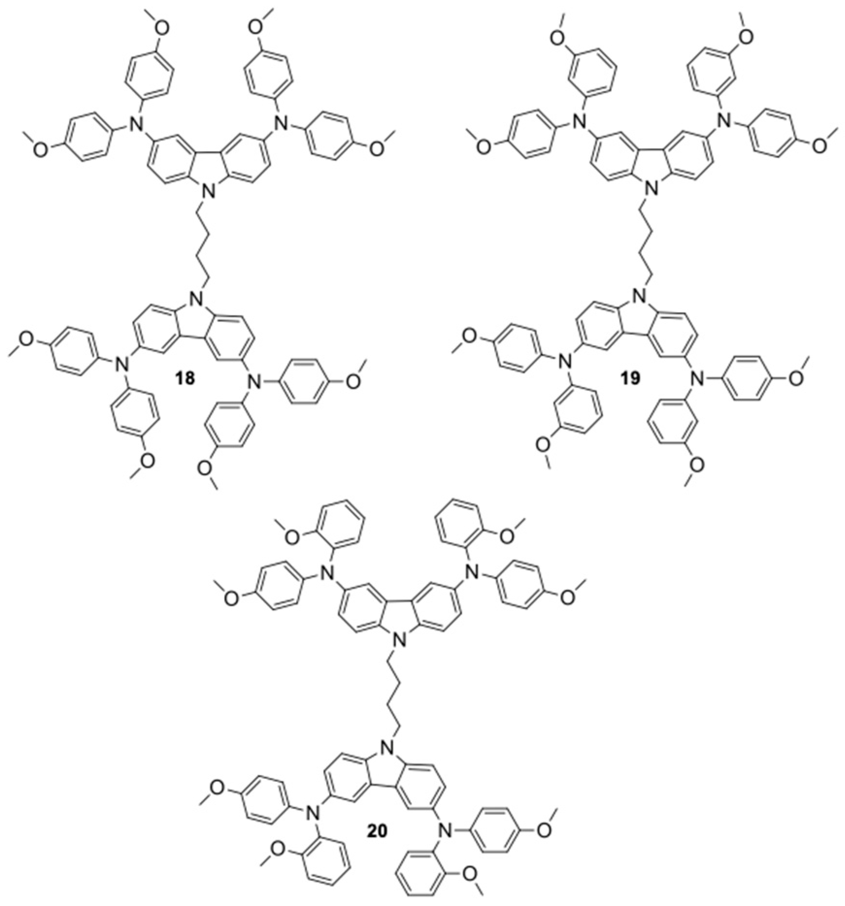
34] reported that branched carbazole cores are important for their applications as HTLs in PSCs, in addition to presenting low cost and high efficiency. Furthermore, they highlighted that ligands that do not present conjugation are not very efficient in the synthesis of organic semiconductors and, consequently, can hinder charge transport. Thus, they prepared three HTLs, named GJ-pp (
18), GJ-pm (
19), and GJ-po (
20), which presented in their structures two carbazole cores connected by a butyl group and four diphenylamine-derived ligands in the 3,6 positions of the carbazole cores. The structures of the three HTLs are represented in
Figure 11.
Under standard solar conditions (Standard Spectrum AM 1.5), the GJ-po (20) structure presented a short circuit current (Jsc) of 22.77 mA.cm−2, an open circuit current (Voc) of 1.022 V and a conversion efficiency (η) of 16.78%. In GJ-pm (39), a short circuit current (Jsc) of 17.09 mA.cm−2, an open circuit current (Voc) of 1.045 V, and a conversion efficiency (η) of 17.09% were observed. However, the structure with the best conversion efficiency was GJ-pp (18), with a short circuit current (Jsc) of 23.22 mA.cm−2, an open circuit current (Voc) of 1.022 V, and a conversion efficiency (η) of 17.23%.
Jegorové et al. [
35] reported, through a series of syntheses of different chromophores bearing carbazole as the central nucleus by means of a one-step palladium-catalyzed Buchwald–Hartwig C–N cross-coupling reaction between 3,6-diaminocarbazole and 2-bromo-N-alkylcarbazoles, in a way that in addition to the photovoltaic properties, these structures have high thermal stability. Thermogravimetric analysis demonstrated that these carbazoles are thermally stable at temperatures higher than 400 °C, which is essential for the processes involved in the production of PCSs. Furthermore, they have higher HOMO (−4.86 eV) and LUMO (−2.11 eV) levels than the conduction and valence bands of typical perovskite materials such as MAPbI3 (MA: methylammonium, VB = −5.45 eV, CB = −3.90 eV).
Jeong et al. [
36] demonstrated a novel application of carbazole derivatives in PSCs of perovskite films based on formamidinium lead triiodide (FAPbI3), which has high efficiency due to a band gap close to the Shockley–Queisser (SQ) limit. However, perovskite materials based on FAPbI3 as the absorber layer have imperfections that induce degradation of their crystal structure at the interface between the perovskite and HTM layers or at the grain boundaries of the light absorber due to contact with the HTM and the absorption of moisture from the ambient air, which shortens their useful life and prevents their efficiency from reaching the theoretical limit (25% efficiency) for this type of solar cell.
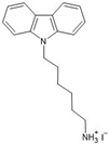
As an alternative to improve these cells [
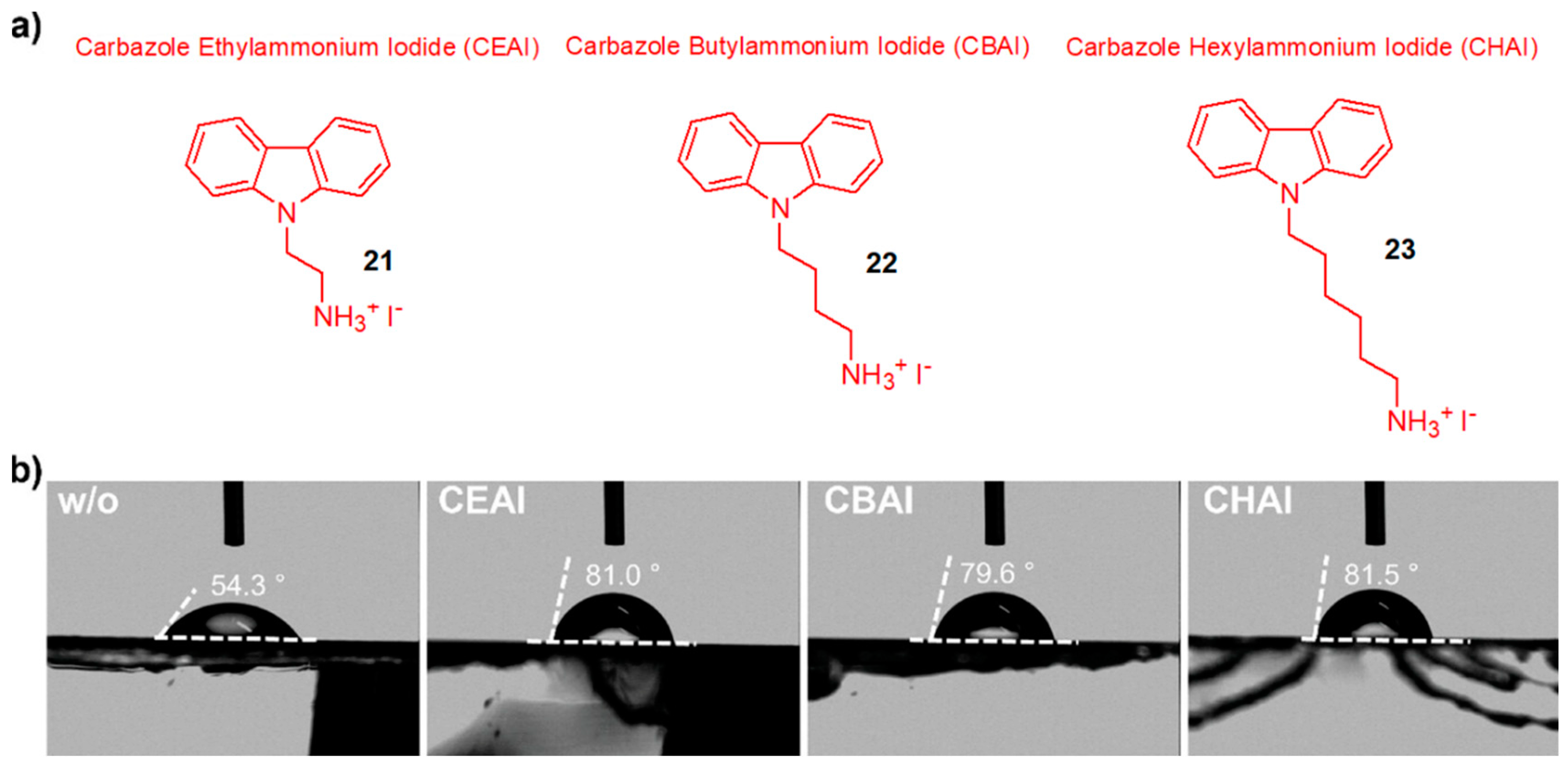
36], passivation using carbazoles modified with ammonium iodide connected by means of alkyl chains of different lengths (ethyl, butyl, and hexyl chains) was proposed, as shown in
Figure 12.
The ammonium group linked to the carbazole through the alkyl chain serves to couple the carbazole to the perovskite surface, which, due to its hydrophobicity, provides greater stability to the perovskite structure and inhibits trap-assisted recombination in perovskite films.
Additionally, the synthesis of these
N-substituted carbazole ammonium salts can be achieved through a carbon–nitrogen cross-coupling reaction starting from halides of alkyl amines [
37].
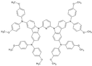
Other studies related to changes in the structure of carbazoles indicate an improvement in photovoltaic performance, such as carbazole molecules substituted by diphenylamine (arm) of the pyridine bridge (core), which attributes more effective optoelectronic properties to PSCs than the HTM of SPIRO-OMeTAD, as they can contribute more to the passivation of defects found in perovskite and in π-conjugation, due to the large amount of delocalized electrons in this core. In addition, HOMO and LUMO energy values were found to be −5.11 and −2.7 eV, respectively [
38].
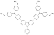
However, simpler carbazole structures that have pyridine linked to the central ring nitrogen have been shown to be more effective than the more complex ones mentioned above—which have a pyridine bridge—as reported by Liu et al. [
39] who developed four triphenylamine–carbazole hole transport materials (HTMs), two with a pyridine and two with a phenyl group linked to the carbazole nitrogen. They found that PSCs based on HTMs containing pyridine increased the efficiency of the photovoltaic cell to 18.45%, compared to 17.81% for PSCs with HTMs based on SPIRO-OMeTAD, due to the bathochromic shift that this ligand causes in the absorption and emission spectra of the triphenylamine-carbazole precursor, resulting in HOMO and LUMO levels (−5.28 and −2.35 eV, respectively) that are more energetically favorable for the transfer of electrons to the perovskite (FAPbI3) 0.85 (MAPbBr3) 0.15, which has a conduction band of −3.92 eV.
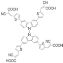
Chalkias et al. [
40] proposed a different approach for the application of carbazoles in DSSCs, where, taking advantage of their versatility, they synthesized di-carbazole molecules as a potential sensitizer for solar cells. This new dye was synthesized with the central core (di-carbazole) as an electron donor and anchoring groups (cyanoacrylic acid) in the TiO
2 semiconductor structure, which serve as bridges in the transfer of electrons between di-carbazole (HTL) and TiO
2 (ETL). The synthesis of the Cz-2 dye was divided into three stages, which involved Suzuki–Miyaura coupling reactions (I) and Knoevenagel condensation (II), as shown in
Figure 13.
The absorption spectrum of the working electrode sensitized by the Cz-2 dye is broad and located in the blue-green region of visible light (400 to 550 nm). This species obtained energy levels of HOMO (−5.89 eV) and LUMO (−3.33 eV), favorable to the electronic transition, which allowed its subsequent application in a DSSC. In addition, through thermogravimetric analysis, it was observed that the prepared di-carbazole presented thermal stability (up to 230 °C) similar to the mono-carbazoles reported by Jegorové et al. [
35], cited above. The
Table 1 shows the data related to the different carbazoles and their respective works.
Apart from their use in solar cells, perovskite photodetectors [
41,
42] are increasingly gaining attention because of their outstanding photoelectric characteristics, such as carrier migration behavior, tunable band gap, and light harvesting capability. The application of perovskites containing carbazoles in the field of photodetectors is still poorly explored, but a recent work reported their use to harvest an optimal detectivity in the visible wavelength by using carbazole-based organic cations in 2D hybrid perovskites as photodiode-type photodetectors [
43].
7. Organic Light-Emitting Diodes (OLEDs)
Contemporary life depends on light-emitting screens. Most homes and businesses around the world have at least one device equipped with a screen (or display) for image reproduction, be it a cell phone, television, monitor, video game, or tablet, among others. Therefore, the development of new technologies in this area is extremely important and attracts a lot of attention from researchers in the academy and industry [
44].
Light-emitting diodes (LEDs) and light-emitting electrochemical cells (LEECs) are widely used nowadays due to their great potential for application in lighting. Due to some limitations arising from liquid crystal devices (LCDs), LED/LEEC technologies have become predominant for the development of light-emitting sources. However, the relatively high production costs of emitting layer components, such as gallium nitride (GaN) and indium gallium nitride (InGaN), have intensified the search for alternative technologies based on organic light-emitting diodes (OLEDs) [
45,
46].
The study and development of OLEDs is still an area with a long way to go for the academic community. They have received a lot of attention due to their promising properties, such as high energy efficiency and color quality, in addition to their lower relative cost when compared to inorganic counterparts. This makes them suitable candidates for large-scale solid-state lighting applications. In addition, the easy processing and a certain versatility in the synthetic modulation of organic materials could enable a new generation of “smart” and flexible displays. However, this technology presents some important challenges that must be solved, including long-term stability and operational stability, especially for materials emitting in the blue region [
47] (JONG, 2019).
Kalyani and Dhobe [
48] remarked that one of the greatest global demands is the search for expanding the electricity generation matrix. OLED panels are called self-illuminating by the industry; that is, each OLED device contained in a panel is responsible for emitting light in each pixel, and an OLED panel is a collection of many individually controlled OLED devices. Thus, a black image means that the device is not emitting light and consequently is not consuming energy for light emission, which makes the device environmentally friendly and saves energy when compared to predecessor technologies (LED, LCD, or Plasma). Even for solid-state lighting, OLEDs are used to replace the lighting system of tungsten or fluorescent lamps, and their use can be a step toward solving energy problems. They are extremely thin and flexible, varying in shapes, colors, and sizes, some even transparent, providing a beautiful ambient glow.
In addition to better image definition, better contrast, better colors, and lower energy consumption, OLED screens can be built with reduced thickness or be foldable. In recent years, emissive OLED screens have gained strength and compete in the market with LCDs in TVs and smartphones because of their unprecedented contrast, smaller thickness, and free form factor [
48,
49].
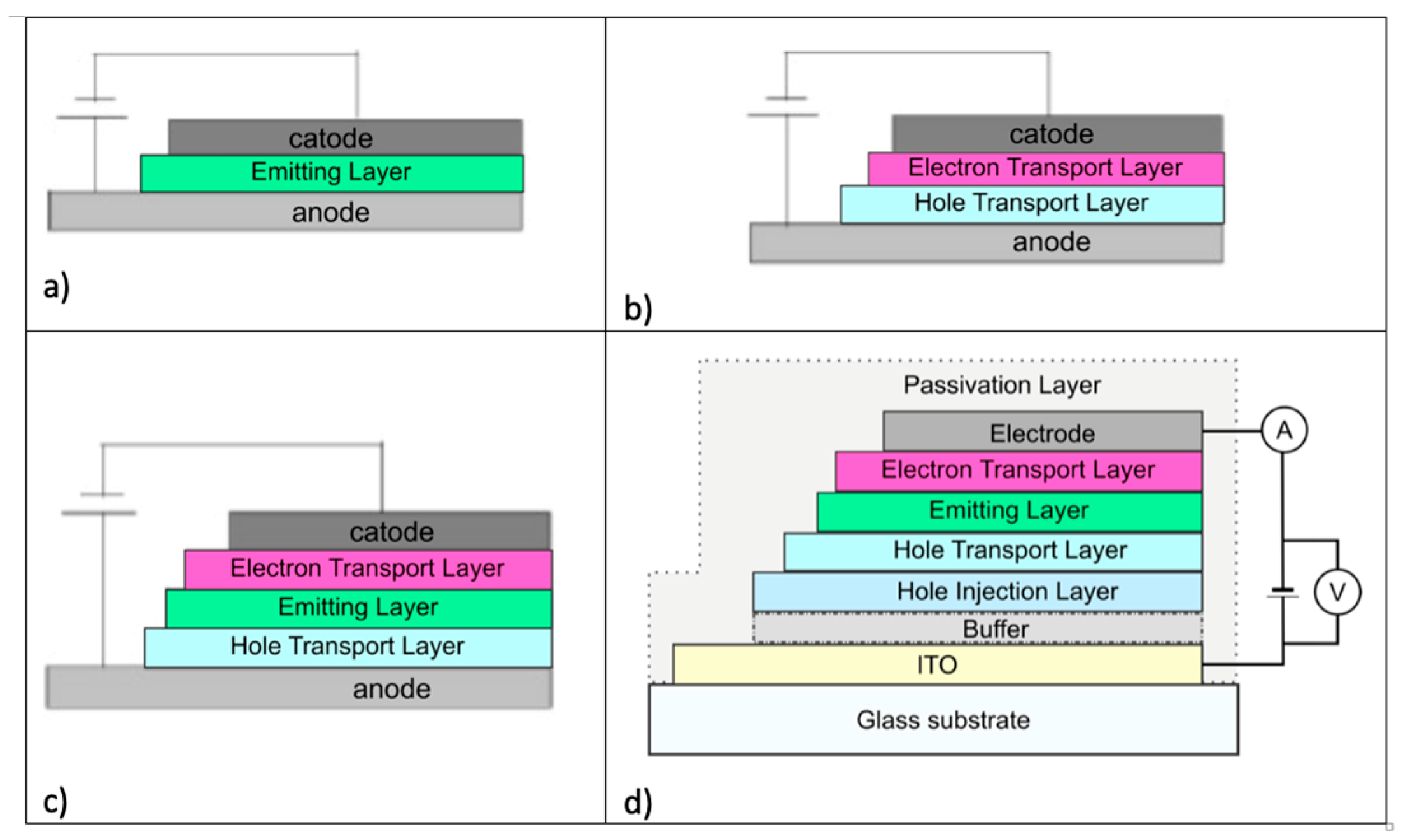
In the structure of materials present in an OLED device, one of the most important components is the semiconductor layer of organic emitting material. Improving emission efficiency with low molar mass materials and better processability for the formation of thin films has been the target of several researches. OLED devices can be arranged in a variety of ways, as their architecture can vary from the number of layers to the way they are deposited on top of each other. In this sense, OLEDs can be structured with layers for hole injection, for hole transport, for light emission, for electron injection and for electron transport. Through a direct approach to describe the fundamental principles of the OLED mechanism, a three-layer structure can be defined as a light-emitting layer (EML) that is positioned between an electron transport layer (ETL) and a hole transport layer (HTL).
In this general mechanism, four steps are crucial for the final light emission. (i) Charge injection: Both electrons and holes are injected from opposite electrodes, the cathode and anode. They represent the negative and positive charges, respectively. (ii) Charge transport: This defines the holes’ and electrons’ migration into the transport layers, HTL and ETL, respectively, before localizing on the emissive molecules in the EML. (iii) Exciton formation: This process involves the combination of a hole on the highest occupied molecular orbital (HOMO) and an electron on the lowest unoccupied molecular orbital (LUMO). (iv) Light emission: When there is the radiative recombination of the exciton, it results in the formation of light, which is visible since it passes through a transparent anode and substrate.
Based on the number of organic layers, we can call OLEDs monolayer, bilayer, trilayer, or even multilayer [
50].
A monolayer OLED is made with only a single organic layer between the cathode and anode. This layer must not only have high quantum efficiency for luminescence but also have good hole and electron transport properties to be able to emit photons [
48]. In a bilayer OLED, one organic layer is specifically chosen to transport holes, and the other layer is chosen to transport electrons. Recombination of the hole–electron pair occurs at the interface between the two layers, which generates electroluminescence [
48]. In a trilayer OLED, an additional layer is placed between the hole transport layer and the electron transport layer. The emitting layer is primarily the site of hole–electron recombination and, thus, electroluminescence [
48]. Finally, In a multilayer OLED, an electron and/or hole injection layer is also included [
48]. In summary, the layers are [
44]:
Substrate—usually a transparent polymer, glass, or metal foil;
Anode—transparent electrode for injecting holes into the organic layers, usually made of indium-doped tin oxide (ITO);
Hole Injection Layer—used for injecting holes from the anode. These are materials with high mobility, electron-blocking capacity, and high glass transition temperature;
Hole Transport Layer—used for transporting holes between the hole injection layer and the emitting layer and for blocking electrons, preventing electrons from reaching the opposite electrode without recombining with the holes;
Emitting Layer—used for transporting electrons/holes and their recombination to form an exciton, which generates light emission. This layer can be composed of a material based on low molecular weight organic molecules or polymers with high emission efficiency, stability, and color purity.
Electron Transport Layer—used to transport electrons between the electron injection layer and the emitting layer and to block holes;
Electron Injection Layer—used to inject electrons from the cathode;
Cathode—typically a metal alloy.
Figure 14 shows the structure of different types of OLEDs.
Concerning the five key parameters involved in the overall performance of OLEDs, it is important to present their definitions. (i) The external quantum efficiency (
EQE) is a useful quantity related to LEDs. It can be defined as the quotient of optical power emitted per electrical input power or the number of photons emitted from the device per electron-hole combined [
51]. (ii) The turn-on voltage, also known as the forward voltage (
Vf), is the minimum voltage related to the OLED light emission in visible and is influenced by the material composition, temperature, and current level, among other factors. (iii) The current efficiency can be defined as the amount of light emitted per unit of electrical current, which is usually measured in candela per ampere (cd/A). (iv) The power efficiency is related to the measurement of the light output involved in the electrical power consumed, which is expressed in lumens per watt (lm/W). (v) The device lifetime is a parameter that concerns the time taken for brightness to degrade to 50% of its initial value under standard operating conditions. In fact, it is the operational durability of the OLED device.
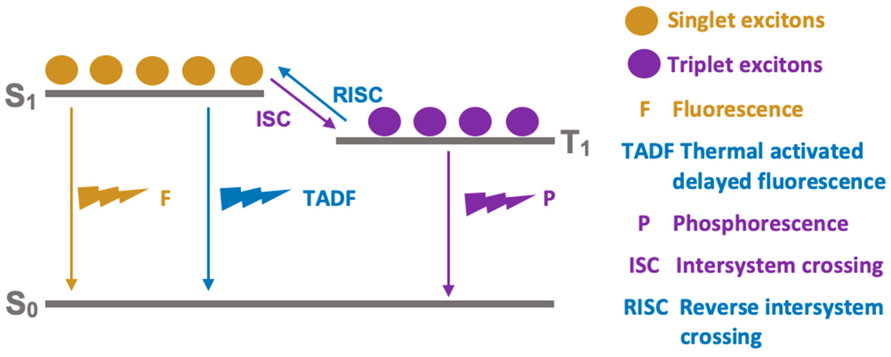
The operating mechanism of an OLED device can be described as follows. When voltage is applied to the device, the cathode supplies electrons and the anode supplies holes to the emitting layer. The electrons and holes migrate from layer to layer until they meet again in the recombination zone, forming pairs of excitons. The exciton is known as a neutral quasi-particle because it is an electron–hole “bound” state that carries energy but has no charge, i.e., a neutral “bound” state. The energy from the excitons can be transferred to the excited states of the material, both singlet (
S1) and triplet (
T1) states. Emission occurs through the decay of these excited states to lower energy states according to the processes shown in
Figure 15. The fluorescence (
F) process is a direct relaxation from
S1 to
S0 states, while phosphorescence (
P) encompasses the intermediate energy
T1 state in the decay process via an Intersystem Crossing (
ISC,
Figure 15). It is important to note that a third exciton relaxation is known, proceeding via a reverse
ISC from
T1 to
S1 and then
S0, and it is known as Thermally Activated Delayed Fluorescence (TADF,
Figure 15). The color of the light depends on the type of organic molecule in the emitting layer and is basically determined by the energy difference between the HOMO and LUMO of the emitting organic material [
48].
In recent years, carbazole-based materials have demonstrated interesting physical properties, including good charge injection and transport, electroluminescence, better thermal and morphological stability, as well as excellent processability during the formation of thin films. In addition, the relatively high level of triplet states of some carbazoles make them suitable candidates for the development of blue, green, and red emitters and as host materials for electrophosphorescent OLEDs [
53]. Thus, carbazole-based compounds (polymeric and low molecular weight derivatives) are among the most studied materials for electronic applications due to the high mobility of holes in their layers and good photoconductive properties.
8. Carbazoles in the Context of OLEDs
Carbazoles, as already described, are versatile compounds widely used as “building blocks” in several electronic applications, but especially in OLEDs. Their ability to tune the properties of organic materials through the combination of different blocks conjugated with π systems makes carbazoles attractive candidates for OLEDs [
54].
They can be used as conventional luminescent emitters, host materials for phosphorescent OLEDs (PhOLEDs), and thermally activated delayed fluorescence (TADF) emitters. The performance of these derivatives is strongly influenced by the molecular design, which directly impacts their electronic and photophysical properties. Next, we will describe how these carbazole derivatives perform these specific functions in OLED devices.
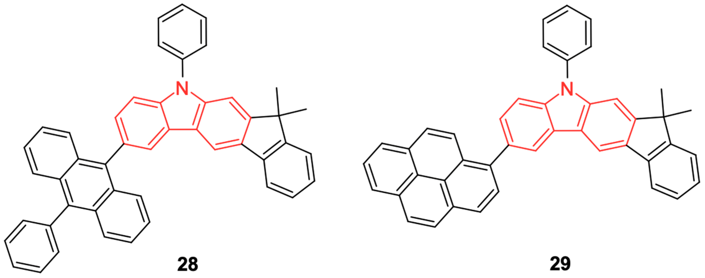
In fluorescent OLEDs, carbazoles contribute as emitting layers to high fluorescence quantum yields; however, the external quantum efficiency (
EQE) is limited since only singlet excitons are used, restricting the maximum theoretical efficiency to 25%. Examples are indolocarbazole derivatives, such as IDC-PA and IDC-Py (
Figure 16), which present high photoluminescence yields (0.84 and 0.78, respectively) and are used in deep blue emission OLEDs; these compounds maintain high efficiency even at high brightnesses [
55].
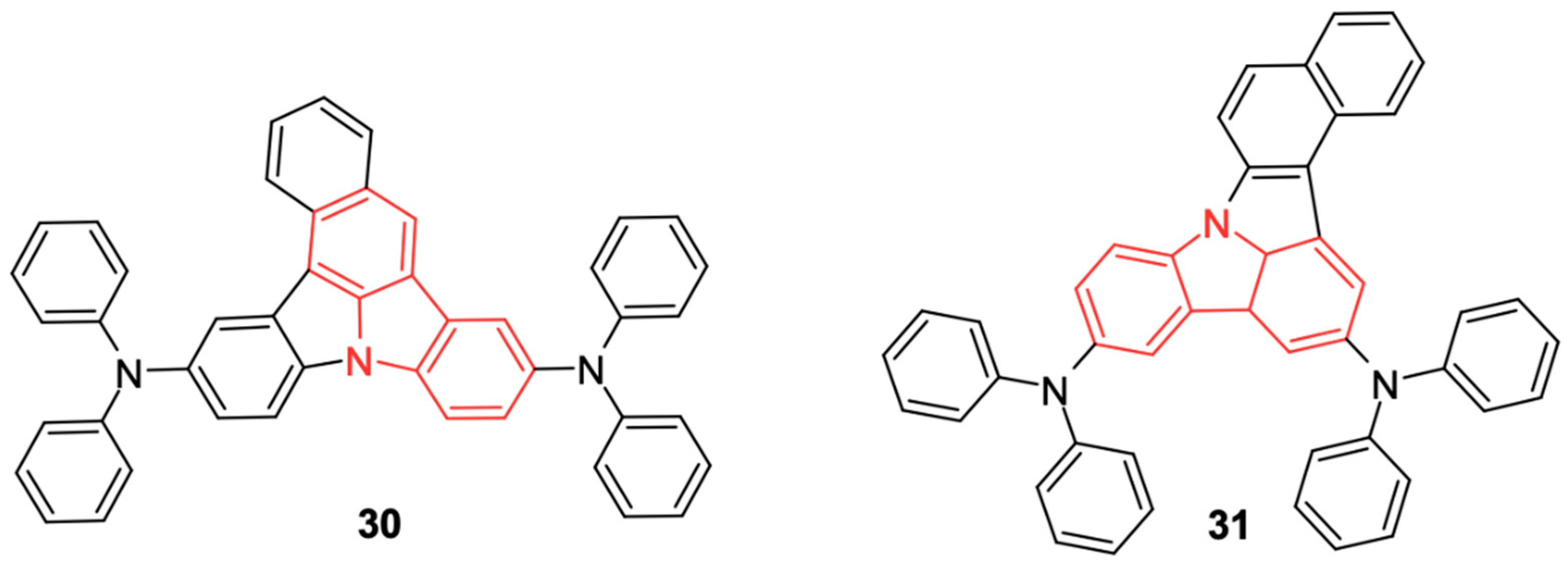
There are also benzocarbazole chromophores, such as NIDPA-1 and NIDPA-2, which can be seen in
Figure 17. These emitters can achieve
EQEs of up to 4.9% in blue OLEDs, presenting high luminance stability, which makes them suitable for practical applications in display technologies [
56].
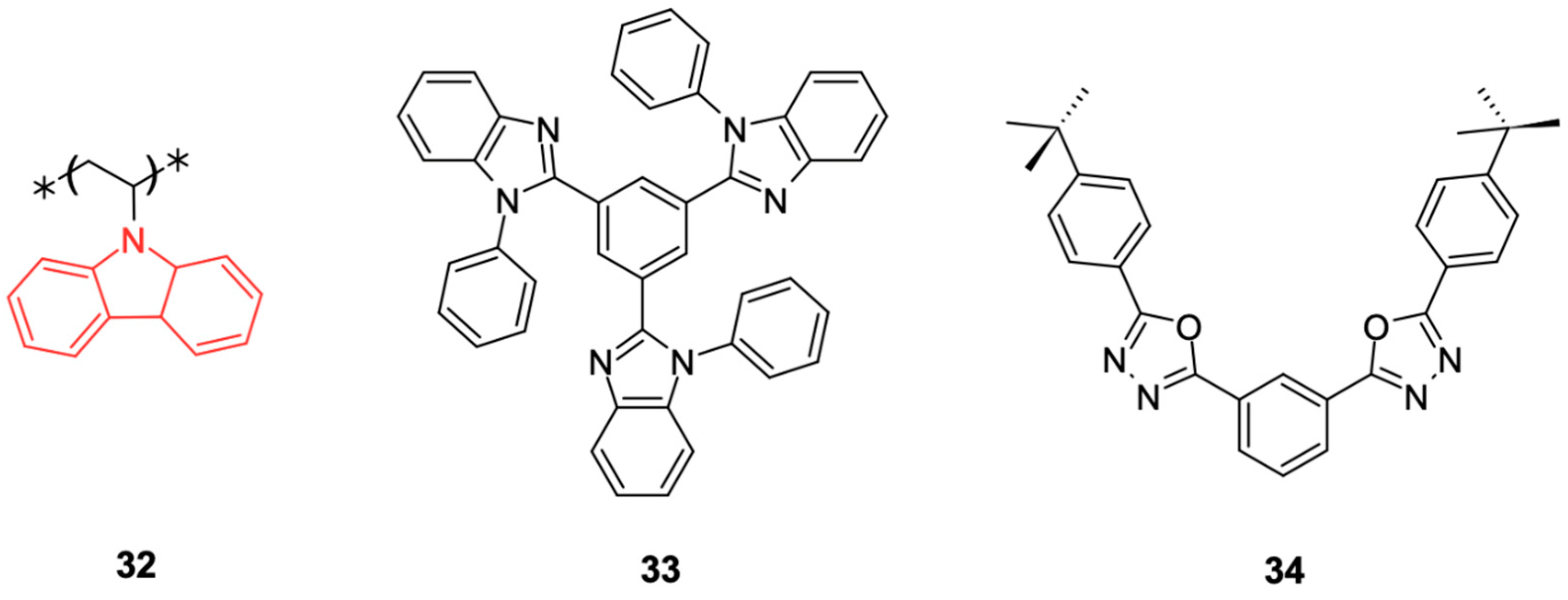
N-Phenylcarbazole derivatives, 3,6-Bis(carbazol-9-yl)-9-(2-ethylhexyl)carbazole (Tris-PCz) and carbazole-based polymers, such as Poly(N-vinylcarbazole) (PVK), although not pure emitters, are often used as host materials due to their electroactive properties. PVK (
Figure 18) has been widely considered as a polymeric host for PLEDs (polymer light emitting diodes) and still constitutes a reference for evaluating the device performance of newly synthesized carbazole-based polymeric hosts. Precisely, the hole mobility of PVK is about 3 orders higher than that of the electron mobility. Electron transport materials that are classically blended with PVK are 1,3,4-oxadiazol-2,2-(1,3-phenylene)bis [5-[4-(1,1-dimethylethyl)phenyl]] (OXD-7) and 1,3,5-tris(N-phenylbenziazol-2-yl)benzene (TPBi) [
57].
Other carbazole derivatives are used as host materials (emitting layers) in phosphorescent OLEDs (PhOLEDs), playing a crucial role in the efficient transfer of triplet excitons to phosphorescent dopants, which improves the efficiency of the devices by taking advantage of both singlet and triplet excitons. There are different types of host materials, such as carbazole bipolar hosts, which combine carbazole donors and triazine acceptors to balance charge transport and avoid triplet exciton quenching, where these materials achieve EQEs higher than 20% in green and red OLEDs [
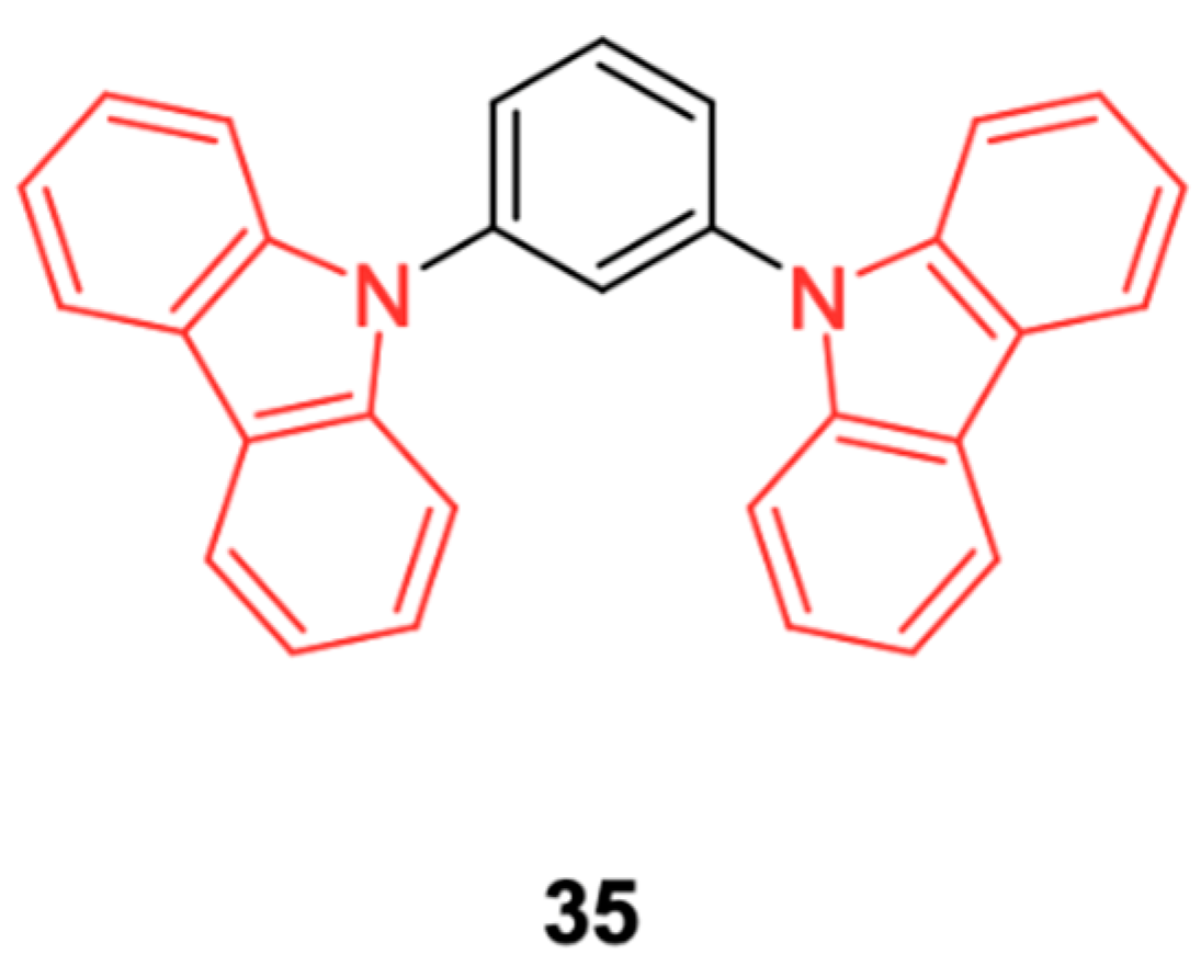
54], and high triplet energy hosts, examples of which include 4,4′-bis(9-carbazolyl)biphenyl (CBP), 1,3-Bis(N-carbazolyl)benzene (mCP), and N,N′-Di(naphthalen-1-yl)-N,N′-diphenylbenzidine (NPB), which, although more common in hole transport layers, can also act as a host material in PhOLEDs. The chemical structure of 1,3-Bis(N-carbazolyl)benzene (mCP) can be seen in
Figure 19.
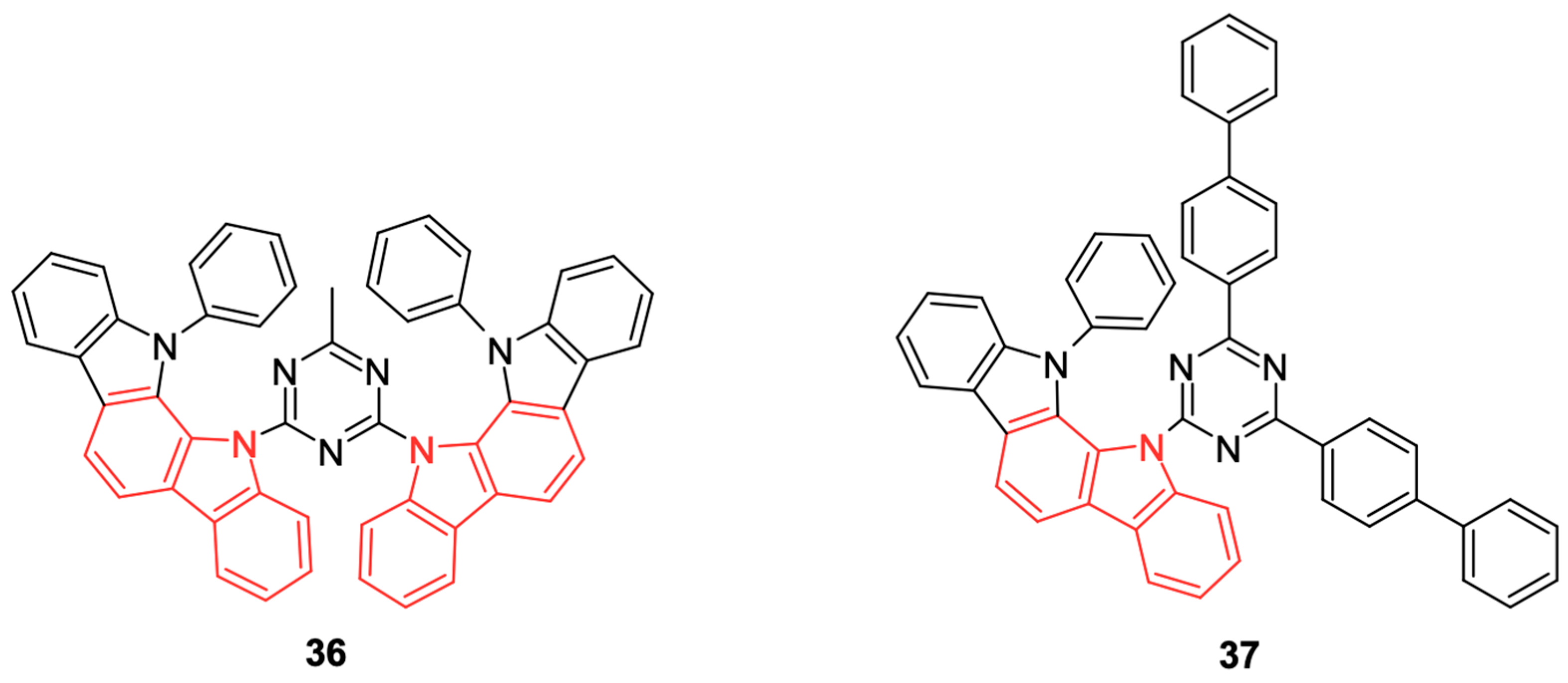
In
Figure 20, indolocarbazole donors combine with a triazine acceptor to obtain BICT, PBICT, POBICT, and BBICT (bipolar carbazole hosts) [
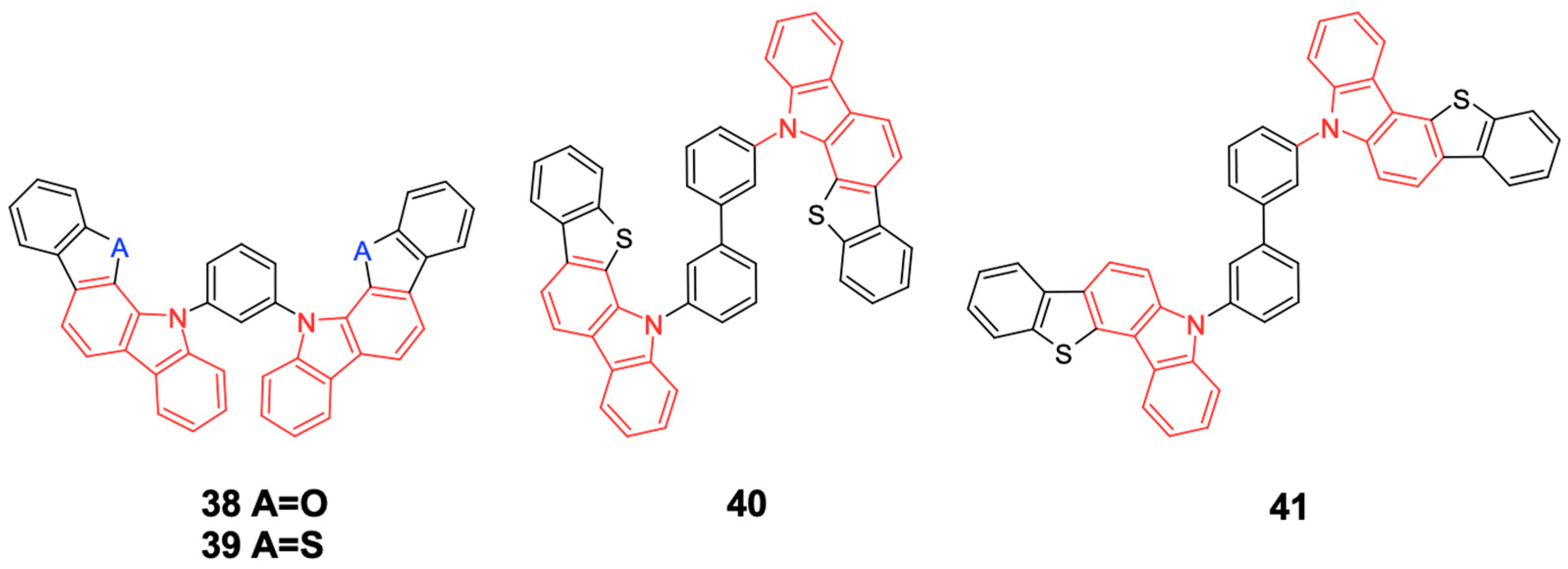
59] can be seen. In
Figure 21, the benzofuran and benzothienocarbazole derivatives BFCz and BTCz, which were designed as analogs of mCP, can be seen. These isomeric benzothieno[3,2-c] carbazole (BTCz) derivatives m1BTCBP and m4BTCBP have been studied as high triplet energy host materials [
60].
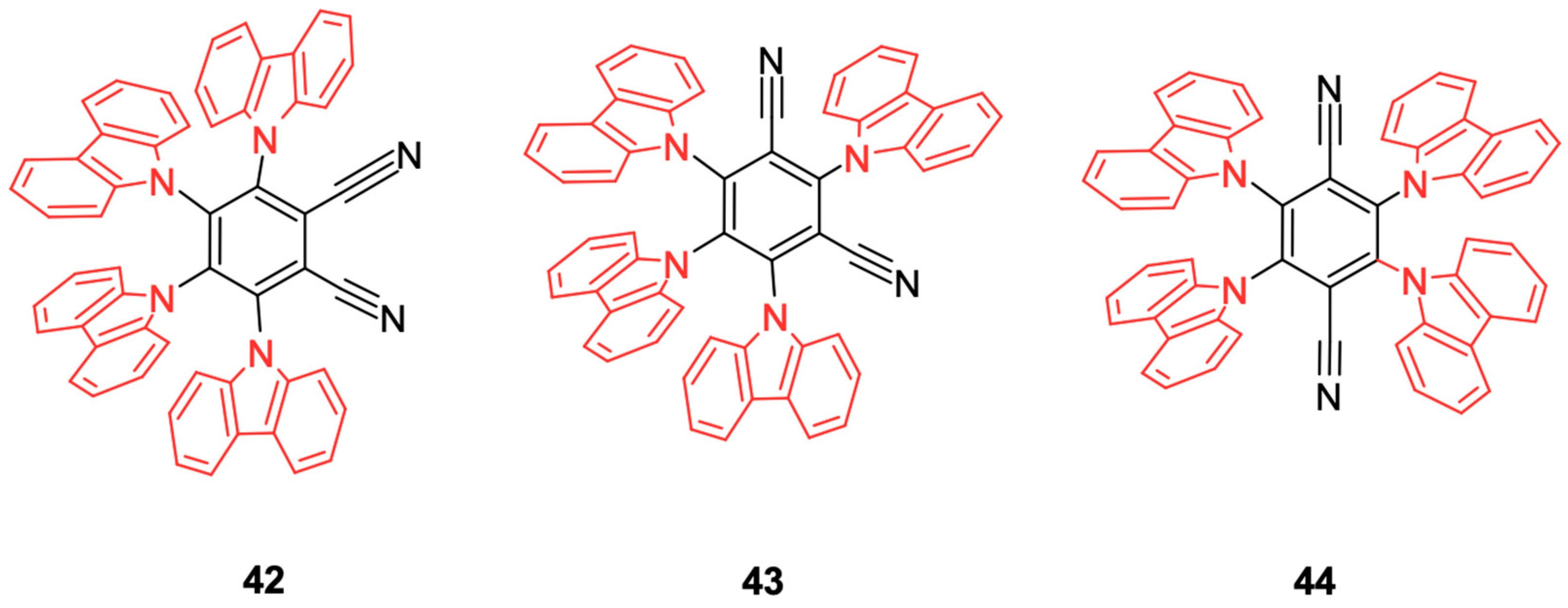
Another type of carbazole derivative used in OLEDs are TADF (Thermally Activated Delayed Fluorescence) emitters. These emitters utilize a donor–acceptor structure, present in carbazoles, to enable reverse triplet-to-singlet conversion (RISC), which can lead to internal quantum efficiencies of up to 100%. There are different types of carbazole-based TADF emitters. For example, carbazole donor–acceptor structures, molecules like DF1 (
Figure 22), which have a small energy difference between the singlet and triplet states, resulting in OLEDs with high external quantum efficiency (
EQE), reaching up to 19.3% for green emissions and 8.0% for blue [
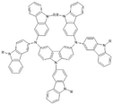
2], and MR-TADF emitters (
Figure 23), which use rigid carbazole-based molecular structures, providing high color purity and narrow emission peaks being ideal for displays requiring vivid and accurate colors [
61].
