Article

A Bidirectional Isolated DC-to-DC Converter with Hybrid Control of Pulse Width Modulation and Pulse Frequency Modulation

1
Department of Electrical Engineering, National Yunlin University of Science and Technology, Douliou 64002, Taiwan
2
Graduate School of Engineering Science and Technology, National Yunlin University of Science and Technology, Douliu 64002, Taiwan
*
Author to whom correspondence should be addressed.
Processes 2024, 12(12), 2866; https://doi.org/10.3390/pr12122866
Submission received: 17 November 2024 / Revised: 10 December 2024 / Accepted: 12 December 2024 / Published: 13 December 2024

Abstract

:
This paper proposes a modified bidirectional isolated DC/DC converter with hybrid control, which can be applied to bidirectional power transfer between energy storage systems and DC microgrids. Batteries are usually applied to energy storage systems. The battery lifespan may be shortened if the converter has large current ripple during the battery charging process. The proposed topology consists of a CLLC converter and an interleaved buck converter. The first stage is an isolated full bridge CLLC converter, and the second stage is an interleaved buck converter with hybrid control of pulse width modulation (PWM) and pulse frequency modulation (PFM). Additionally, the proposed topology achieves zero voltage switching (ZVS) for all switches and reduces the output current ripple. The operational principles of bidirectional power flow in both directions are described in detail. Finally, a 1.5 kW experimental prototype, rated with a high side voltage of 380 V and low side voltage range of 40–58 V, was constructed and tested to investigate the system performance. The measured highest efficiency for the proposed converter is 90% in charging mode, and 94% in discharging mode.

1. Introduction

With the advancement of technology and the increasing demand for energy, it is important to recognize the need for efficient energy utilization. Excessive reliance on non-renewable energy sources has led to serious environmental pollution. The growing awareness of environmental protection has driven the development of renewable energy sources worldwide. As renewable energy usage increases, the role of DC power systems and DC microgrids [1,2] with energy storage systems (ESSs) becomes essential for enhancing power quality, conversion efficiency, and the reliability of power generation. Therefore, energy conservation is a primary concern in this industry. Improving the efficiency of power converters is a key objective to achieve this goal. ESSs typically consist of a battery operating at a lower voltage than the DC bus. A bidirectional DC/DC converter is used to charge and discharge the battery set of an ESS. Enhancing the efficiency and power density of bidirectional DC/DC converters is crucial for enabling residential energy storage systems. Additionally, galvanic isolation is necessary to guarantee converter safety, usually achieved through the implementation of an isolated converter topology such as dual-active-bridge (DAB) converters, LLC converters, and CLLC converters.
The DAB converters [3,4,5,6] use the leakage inductance of the high-frequency transformer as the power transfer element thereby increasing power density with simple control requirements. However, DC sources such as energy storage systems, Li-Ion Battery, or renewable energy sources have wide voltage variations, leading to a limited zero voltage switching range and high circulating current, especially at light loads. Ensuring soft switching across the entire load range was proposed through complex modulation involving three or more control variables [7,8]. However, this approach complicates the controller implementation and necessitates an offline optimization to select the optimal combination of variables.
The isolated bidirectional LLC [9,10,11] and CLLC resonant DC/DC converters [12,13,14,15,16,17] consist of dual bridges and resonant tanks. Compared to the DAB converter, resonant converters have a wider zero voltage switching (ZVS) load range, which leads to higher efficiency. Nevertheless, resonant converters may suffer the problem of reduced efficiency when the switching frequency is deviated from the resonant frequency. Therefore, resonant converters may not operate in optimal condition at the entire load range if the converter is designed as a single-stage structure.
In [9], the proposed topology can overcome the problem of circulating current when the LLC converter operates at its resonant frequency. However, this topology incorporates two sets of LLC resonant tanks, which increases the number of switches and could potentially reduce the overall efficiency of the converter. Ref. [14] presents a detailed design procedure for a CLLC-type resonant converter for battery charging, ensuring soft-switching in all switches and enabling high-frequency operation. The design methodology includes determining transformer turns ratio, magnetizing inductance design, and calculating resonant inductance and capacitance.
In [17], a hybrid control strategy is proposed. This innovative control strategy combines pulse frequency modulation (PFM) and phase-shift modulation (PSM) to achieve high efficiency and stable operation. The proposed control can be easily implemented using a digital signal processor, making it a practical solution for power electronics applications. These circuit topologies offer several advantages such as soft switching, wide voltage gains, and minimized circulating currents. However, CLLC converters have a large output ripple, which may reduce battery life.
To deal with the issue of output ripple, a two-stage circuit was implemented, in which the second stage circuit adjusts the output voltage [18,19,20,21]. Ref. [22] introduces a digital adaptive control for a bidirectional DC/DC charger/discharger; this method achieves ZVS [23,24,25,26,27,28] without the need for an auxiliary zero-crossing detection (ZCD) circuit. It determines the appropriate switching frequency through digital calculation to satisfy ZVS conditions, allowing for soft switching over a wide range of input and output voltages. Although using a two-stage circuit increases the number of components, which may slightly decrease overall efficiency, it allows for an extension of the output voltage range and a reduction in output ripple.
This paper proposes a modified bidirectional isolated DC/DC converter with hybrid control, as illustrated in Figure 1. The first stage circuit is a full bridge CLLC converter that functions as a transformer to achieve galvanic isolation and uses an open-loop fixed frequency control to reduce electromagnetic interference. This topology facilitates the achievement of ZVS and zero current switching (ZCS) thereby improving the overall efficiency of the converter. The second stage circuit is an interleaved buck converter that employs pulse width modulation (PWM) and PFM controls to extend the output voltage range and enhance converter efficiency under light load conditions. The proposed approach allows for an expanded output voltage range and reduced output current ripple. The article is organized as follows: In Section 2, the operational principles and hybrid control strategy are described in detail. In Section 3, the circuit parameters are designed, and an experimental prototype is built and tested to verify the theoretical analysis. Finally, the conclusion is presented in Section 4.

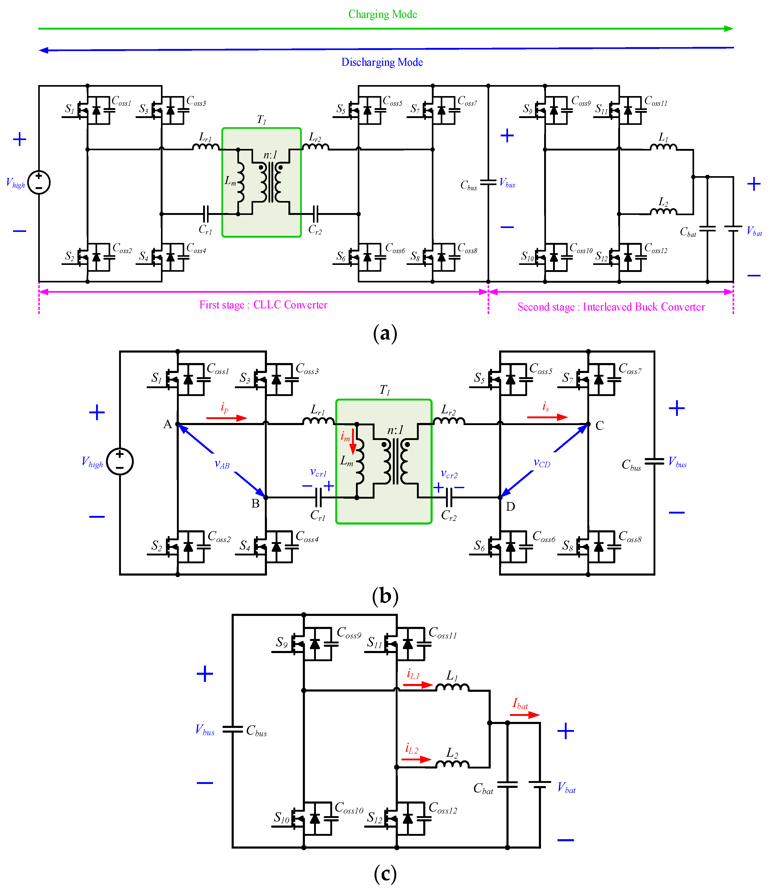
2. Proposed Bidirectional Converter and Operation Principle

The proposed bidirectional isolated DC/DC converter with hybrid control is shown in Figure 1. The power flow is transferred from Vhigh to Vbat when the converter is operating in charging mode. In the discharging mode, the converter operation is reversed. Since the operation principles of the converter are similar in both charging and discharging modes, only the analysis of the operation principle for the proposed converter in the charging mode will be presented. In this article, the analysis of the first stage circuit and the second stage circuit will be provided.

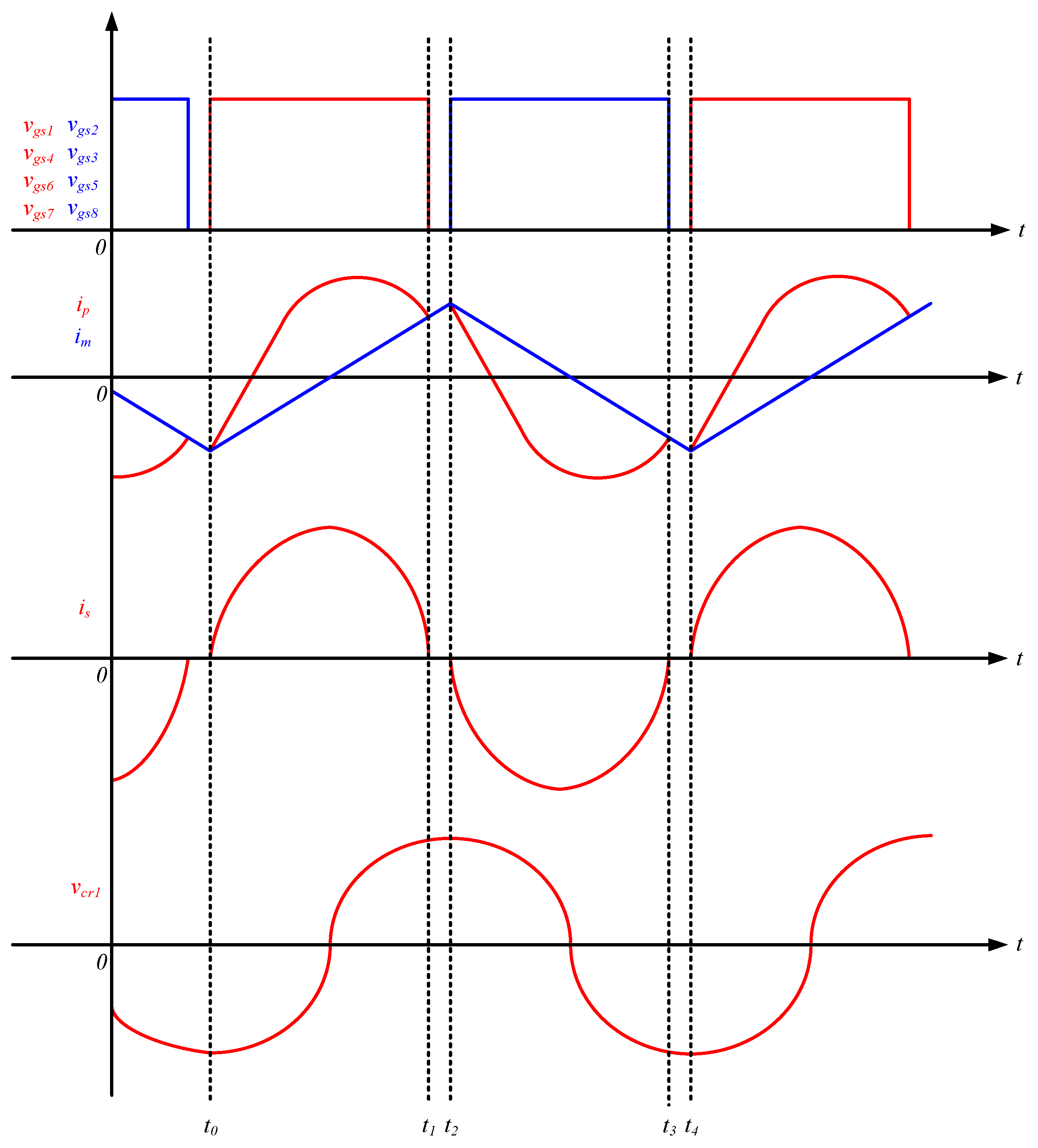
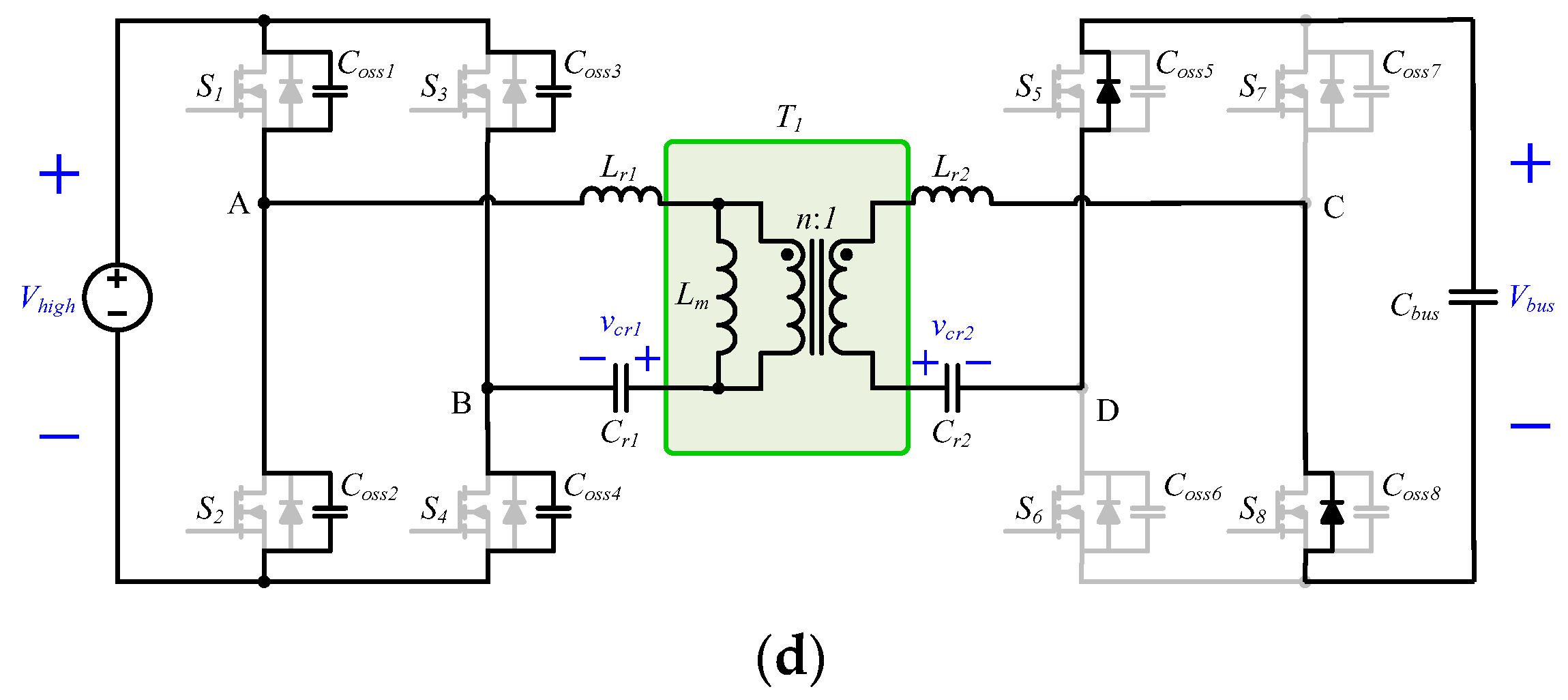
2.1. CLLC Resonant Converter

The CLLC resonant converter, as illustrated in Figure 1b, is capable of bidirectional power transfer. In charging mode, the direction of power flow is transferred from the Vhigh to the Vbus, and vice versa in discharging mode. The CLLC converter comprises two full bridge circuits and the resonant tank including Lr1, Cr1, Lm, Lr2, and Cr2. The primary side bridge functions as a high-frequency inverter, while the secondary side bridge performs rectification in charging mode. In discharging mode, the roles of these two full bridges are reversed.
Therefore, the resonant frequency fr, the quality factor Q, and the inductance ratio k, are obtained as follows:
f r = 1 2 π L r 1 C r 1
Q = Z r R o , e
k = L r 1 L m
where the characteristic impedance Zr and equivalent resistance of resonant network Ro,e are given by
Z r = L r 1 C r 1
R o , e = 8 n 2 π 2 R o
As shown in Figure 2, the operation of the CLLC resonant converter can be divided into four stages. The operations of Stages 1–4 are presented as follows:
Stage 1 [t0t1, Figure 3a]: In Stage 1, S1, S4, S6, and S7 are turned on, and S2, S3, S5, and S8 are turned off. The inductor current flows through the secondary resonant inductor and capacitor to the Vbus. In this mode, the resonant current ip flows through the resonant inductor and capacitor, changing its direction from negative to positive.
Stage 2 [t1t2, Figure 3b]: S1, S4, S6, and S7 are turned off and the CLLC converter enters into the duration of dead time. The voltage of parasitic capacitors Coss1 and Coss4 are charging from zero to Vhigh. Meanwhile, the voltage of parasitic capacitors Coss2 and Coss3 are discharging from Vhigh to zero. At this stage, the primary side current ip decreases, and the primary current commutation is completed. The stage ends when S2, S3, S5, and S8 are turned on.
Stage 3 [t2t3, Figure 3c]: In Stage 3, S2 and S3 are turned on under ZVS condition. Energy is transmitted to the secondary side through the transformer. During this stage, the primary side current ip flows through the resonant inductor and capacitor, reversing the direction from positive to negative.
Stage 4 [t3t4, Figure 3d]: In this stage, the operation principle is similar to Stage 2. The difference between Stage 4 and Stage 2 is that the voltage of Coss1 and Coss4 discharges to zero and the voltage of Coss2 and Coss3 charges to Vhigh. When S1, S4, S6, and S7 are turned on, this stage ends.

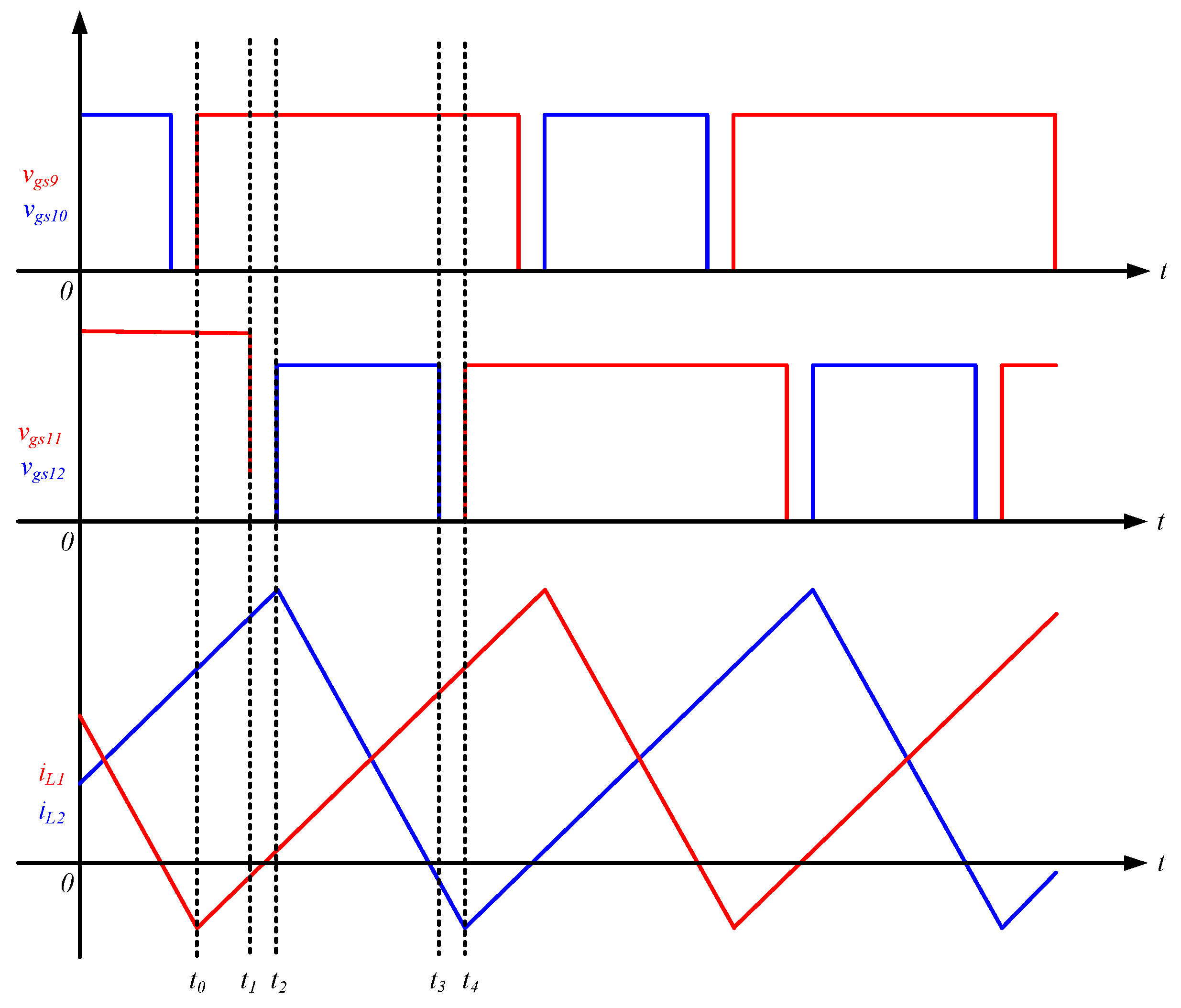
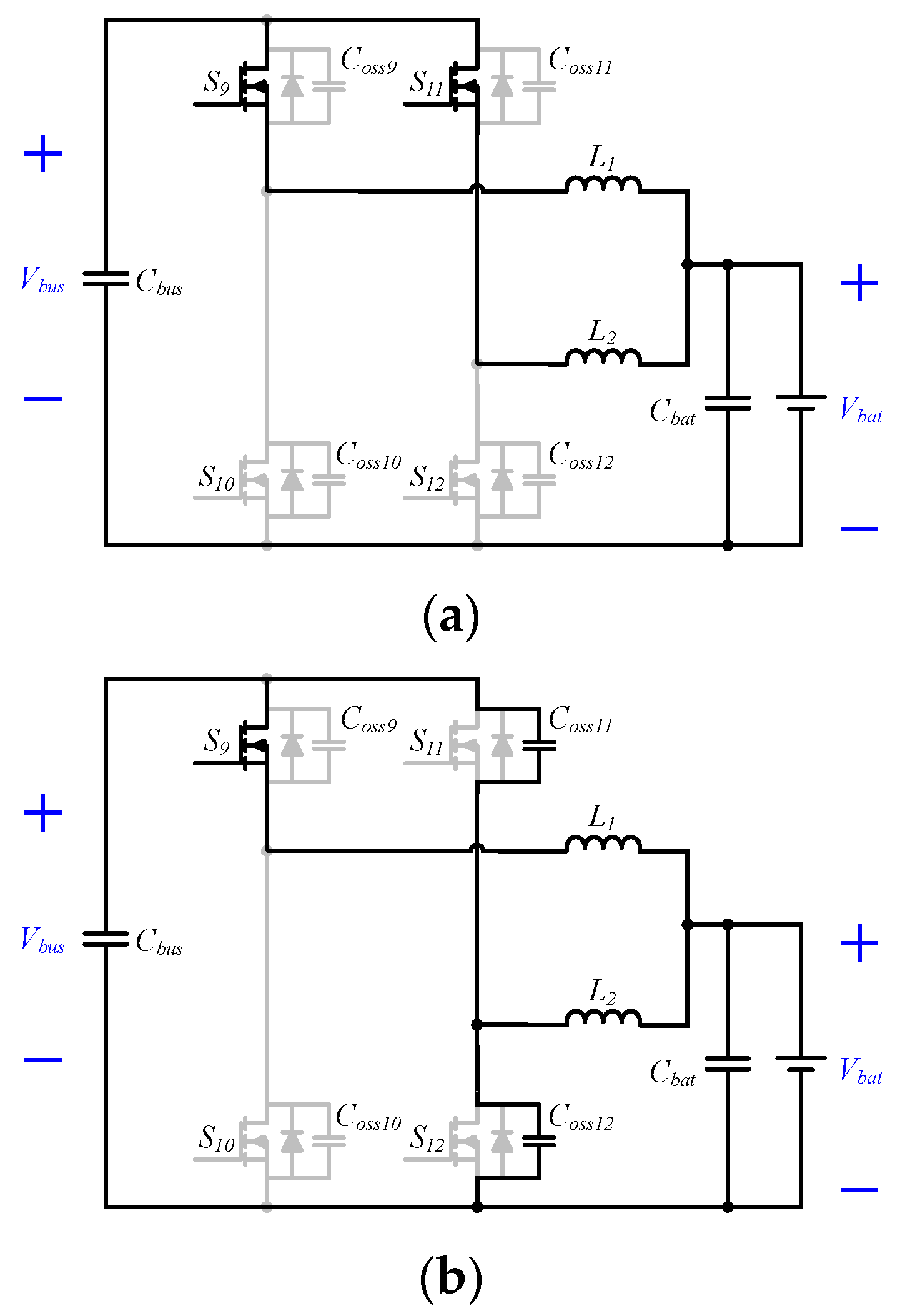
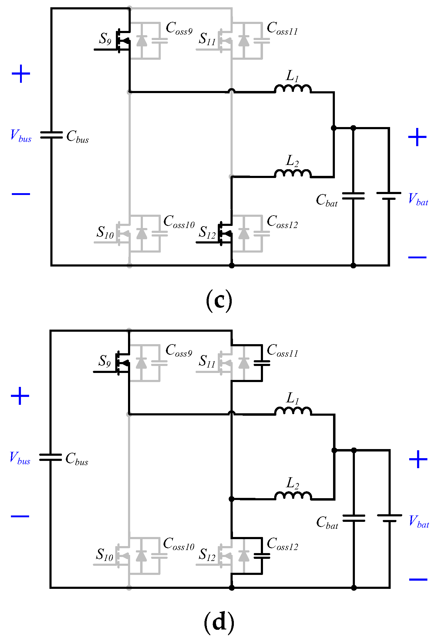
2.2. Interleaved Buck Converter

The interleaved buck converter, as illustrated in Figure 1c, is capable of bidirectional power transfer between Vbus and Vbat. The proposed converter is operated in boundary conduction mode (BCM) using hybrid control to reduce inductor current ripple, enabling S9 to S12 achieve ZVS. The operation of the main structure can be divided into eight stages. The operations of Stages 1–4, as shown in Figure 4, are similar to that of Stages 5–8 thus only Stages 1–4 are presented.
As shown in Figure 4, S9 and S10 are complementary, as are S11 and S12. The two sets of signals are driven with a phase-shift of 180 degree. The inductor currents are interleaved to reduce output current ripple.
In this circuit, the average current of each phase can be obtained by
I L , a v g = I b a t N p h a s e
The peak inductor current IL,peak can be expressed as follows:
I L , p e a k = 2 ( I L , a v g + I R )
Using the inductor volt-second balance, the equations for calculating the duty cycle Dbuck, and switching frequency fsw,buck of the interleaved buck converter can be obtained as follows:
D b u c k = V b a t V b u s
f s w , b u c k = V b a t ( V b u s V b a t ) L V b u s I L , p e a k
By substituting IL,peak into Equation (10), the required inductor value for the circuit can be obtained from Equation (10).
L = L 1 = L 2 = V b a t ( V b u s V b a t ) f s w , m i n V b u s ( I L , p e a k + I R )
Stage 1 [t0t1, Figure 5a]: In Stage 1, S9 and S11 are turned on, and S10 and S12 are turned off. The inductor current iL1 and iL2 will increase to the maximum value.
Stage 2 [t1t2, Figure 5b]: This stage is the dead time between S11 and S12. S11 is turned off, and the inductor L2 changes from stored energy to release energy. The inductor L1 still stores energy.
Stage 3 [t2t3, Figure 5c]: S12 turns on under ZVS condition. The inductor L2 releases energy. The inductor current iL2 decreases linearly to the minimum value.
Stage 4 [t3t4, Figure 5d]: This stage is similar to Stage 2. S12 turns off, the inductor L2 changes from released energy to stored energy.

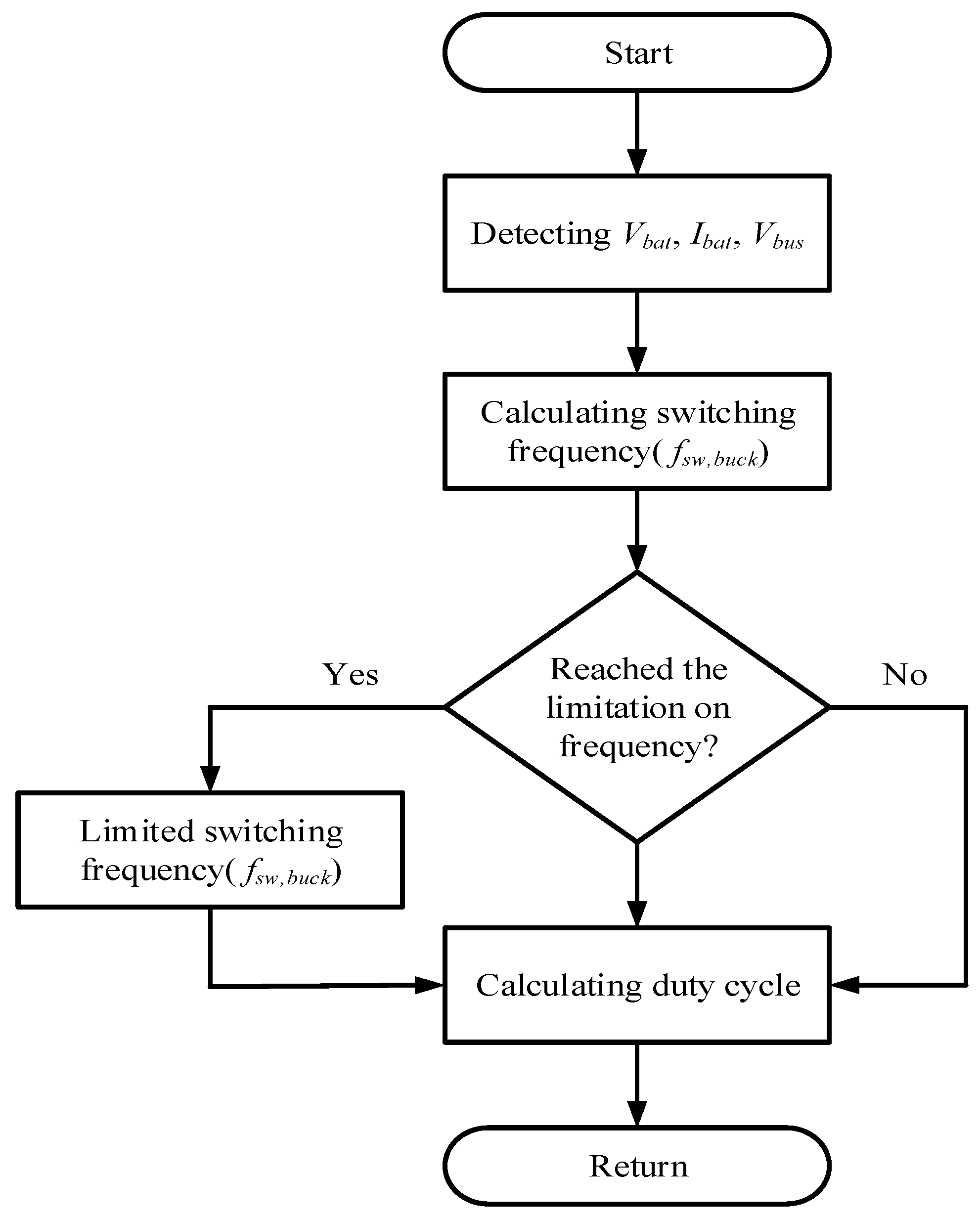
2.3. Proposed Digital Hybrid Control

A flowchart of the hybrid control is illustrated in Figure 6. The proposed digital hybrid control combines PWM with PFM and is implemented using the digital signal processor (DSP) TMS320F28335. An analog-digital-converter (ADC) module is used to detect the Vbat, Ibat, and Vbus.
When the circuit parameters and operating conditions are defined, the switching frequency primarily dictates the operating mode of the converter. If the switching frequency is too high, the interleaved buck converter operates in continuous conduction mode (CCM), resulting in the loss of ZVS for the switches. It is less efficient due to increased switching losses. Conversely, if the switching frequency is too low, the converter generates a higher circulating current, leading to increased conduction losses, which also adversely affects the converter efficiency. Therefore, selecting an appropriate switching frequency based on the specific operating conditions is crucial to ensure that the converter can operate under various load conditions efficiently and increase the proposed converter performance and reduce power losses.
For balancing the trade-offs between switching losses and conduction losses to achieve possible maximum efficiency, the interleaved buck converter can operate in BCM. According to Equation (9), the inductance value and battery voltage are used to calculate the maximum and minimum values of fsw,buck. The maximum and minimum values of fsw,buck are set as the upper and lower boundary of the switching frequency. If the calculated result is over the boundary, fsw,buck will be limited at the maximum or minimum value and the modulation will be changed from PFM to PWM. Conversely, the PFM is used continually.

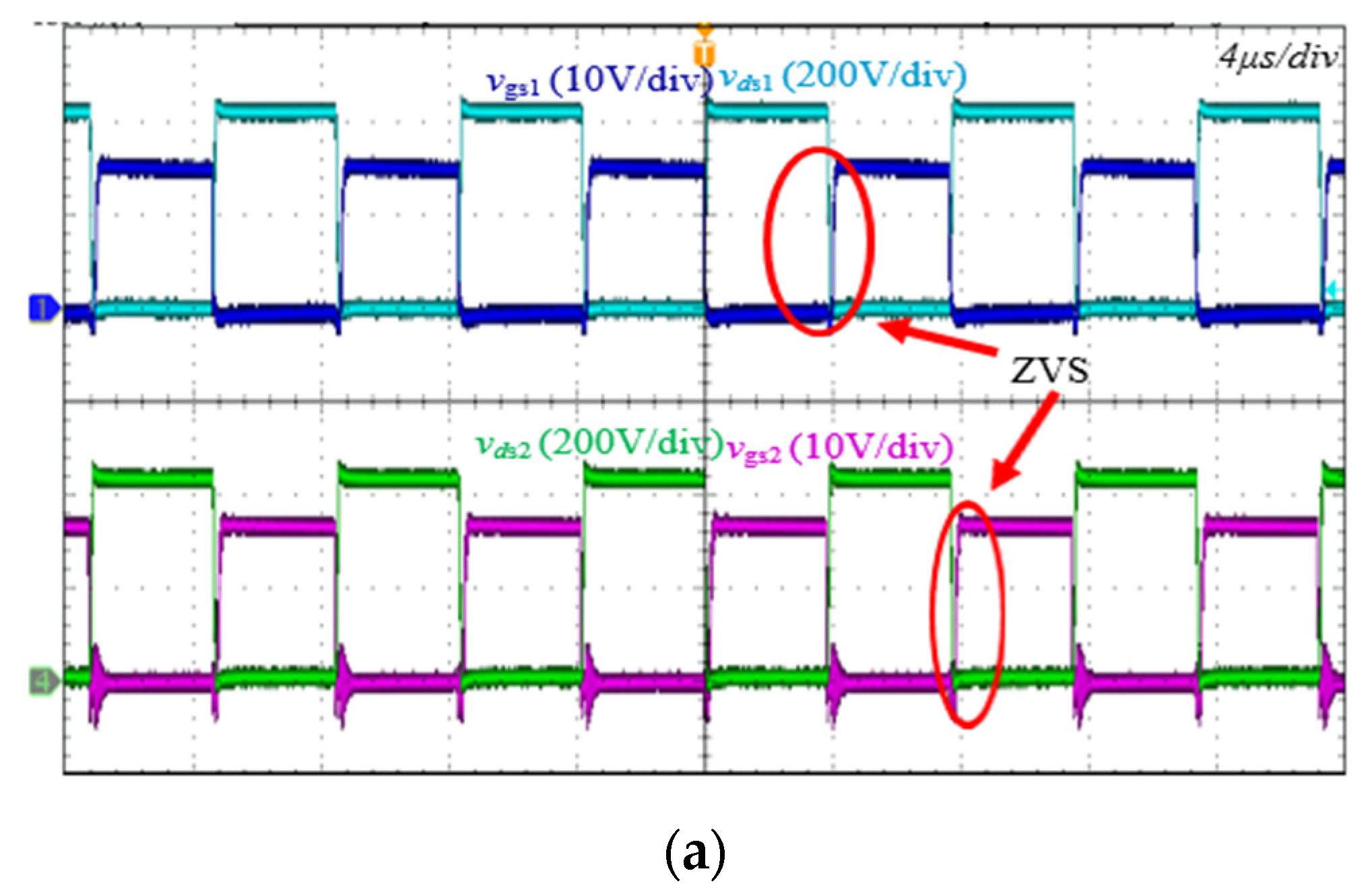
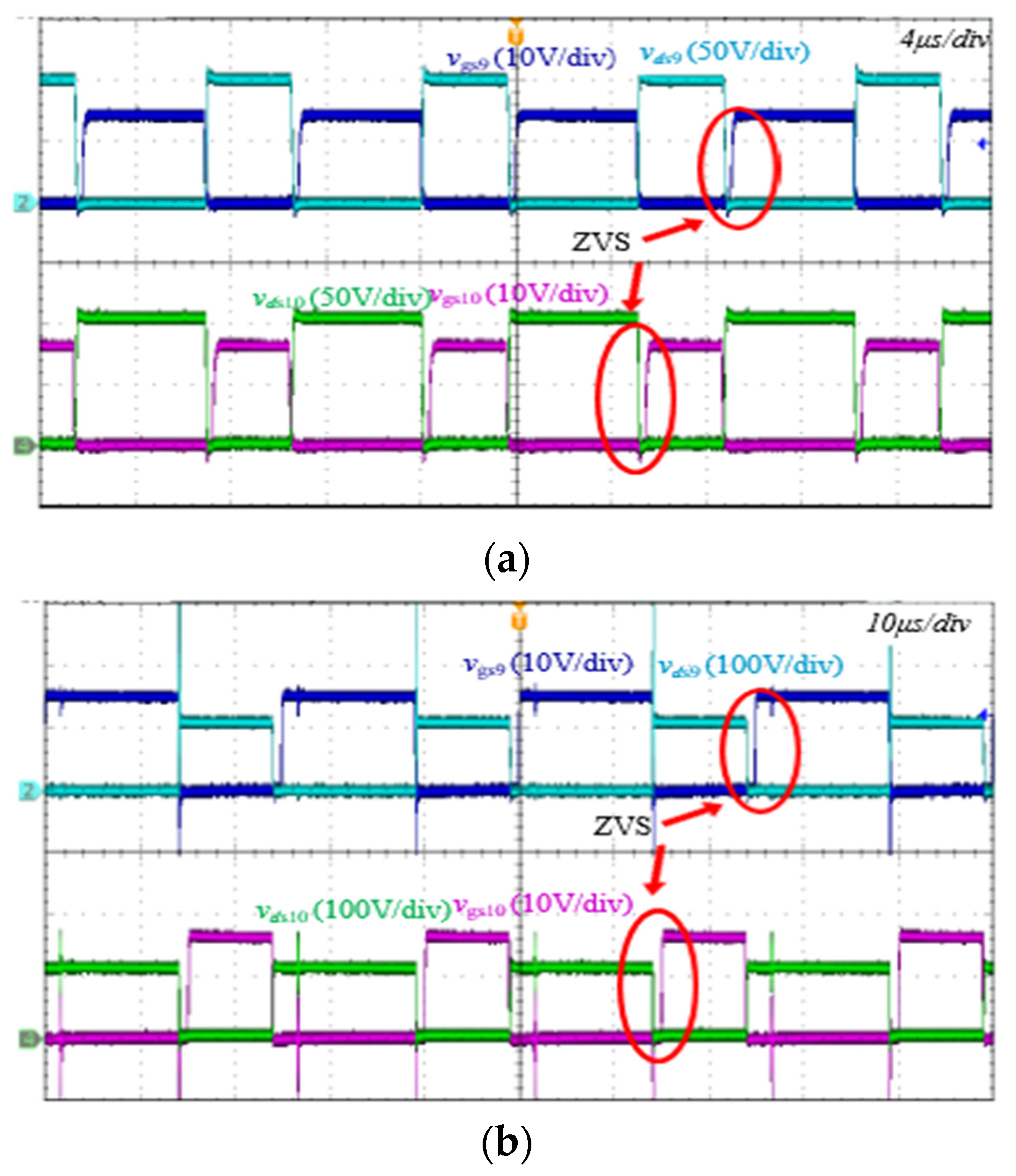
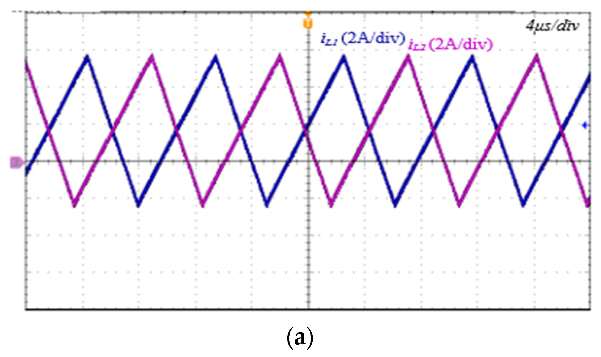
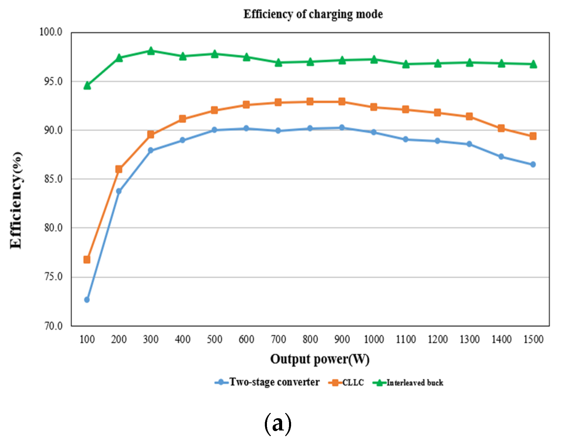
3. Experimental Results

Based on the design conditions described in Section 2, a 1.5 kW experimental prototype incorporating the proposed digital hybrid control was constructed to verify the converter performance. The high side voltage of the converter ranges from 380 to 400 V, and the battery voltage ranges from 40 to 58 V. The switching frequency of the first stage CLLC converter is 130 kHz, while the switching frequency of the second stage interleaved buck converter is between 40 kHz and 110 kHz. The parameters of the proposed converter are listed in Table 1.
Figure 7, Figure 8, Figure 9 and Figure 10 show the experimental waveforms for the proposed converter with output power 150 W (10% of full load) and 1.5 kW (full load) in charging mode. Figure 7 and Figure 8 show that the CLLC converter can achieve ZVS when operating under a light load and full load conditions. Figure 9 and Figure 10 show that the interleaved buck converter can operate at different switching frequencies with different loads. Figure 10 shows the current waveforms of the inductors L1 and L2. The two-phase interleaving operation of the proposed converter can be achieved effectively, which significantly reduces output current ripples, thus enhancing system overall performance and stability.
The efficiency curves of the proposed converter are shown in Figure 11. The blue line represents the efficiency of the proposed converter, the orange line shows the efficiency of the first stage CLLC converter, and the green line indicates the efficiency of the second stage interleaved buck converter. Because the proposed converter is a two-stage topology, the efficiency equation of the converter in both modes can be expressed as follows:
η o v e r a l l = η C L L C η b u c k
It was found that the proposed interleaved buck converter is more efficient than the traditional converter under light load conditions. This efficiency improvement in both charging and discharging modes enhances the overall performance for the proposed converter. The maximum efficiency of the proposed converter is 90% in charging mode and 94% in discharging mode.
The proposed converter was compared to different converters with similar voltage gain in [3,29,30] and the converter of two-stage topology was compared in [31], as shown in Table 2. Although the proposed converter uses more components than the converter in [3,10,29,30,31], the output power of proposed one is higher. Compared with [3,10,17,30], although they have higher efficiency, the higher output current ripple will lead to a reduced lifespan of the ESS.

4. Conclusions

This paper has presented a modified bidirectional isolated DC/DC converter with hybrid control to enhance power conversion efficiency and performance. The proposed converter integrates a CLLC resonant converter in the first stage and an interleaved buck converter in the second stage, resulting in significant efficiency improvements and high operational stability. The hybrid control combining PWM and PFM techniques enhances light load efficiency for the converter by balancing switching and conduction losses. The CLLC converter achieves ZVS under light load and full load conditions, while the interleaved buck converter reduces output current ripples at different switching frequencies and various loads. Efficiency curves show the proposed converter achieved a maximum efficiency of 90% in charging mode and 94% in discharging mode. Even though the proposed converter used more components, the efficiency of the converter in both charging and discharging modes make it ideal for bidirectional power transfer in the applications of energy storage systems and DC microgrids.

Author Contributions

C.-C.H. and J.-B.L. conceived and designed the prototype circuit; J.-B.L. performed simulations and experiments and analyzed data; C.-C.H. contributed equipment, materials, and analysis tools; J.-B.L. wrote the paper; C.-C.H. revised the paper. All authors have read and agreed to the published version of the manuscript.

Funding

This research was supported by the National Science and Technology Council of Taiwan under grant number MOST 112-2221-E-224-004.

Data Availability Statement

The original contributions presented in this study are included in the article. Further inquiries can be directed to the corresponding author.

Conflicts of Interest

The authors declare no conflicts of interest.

Abbreviations

IL,avgAverage current of each phase
IbatBattery current
VbatBattery voltage
VbusBus voltage
ZrCharacteristic impedance
iL(n)Current of nth inductance
DbuckDuty cycle of interleaved buck converter
η C L L C Efficiency of CLLC converter
η b u c k Efficiency of interleaved buck converter
η o v e r a l l Efficiency of proposed converter
Ro,eEquivalent resistance of CLLC converter
vgs(n)Gate-source voltage of nth switch
VhighHigh side voltage
kInductance ratio
RoLoad resistance of CLLC converter
LmMagnetizing inductance
imMagnetizing inductance current
fsw,minMinimum switching frequency of interleaved buck converter
NphaseNumber of phases used in interleaved buck converter
PoOutput power
Coss(n)Parasitic capacitance of n-th switch
IL,peakPeak inductor current
IRPeak inductor reverse current
ipPrimary side current
QQuality factor
Cr(n)Resonant capacitance with nth
frResonant frequency of CLLC resonant converter
Lr(n)Resonant inductance with n-th
isSecondary side current
fsw,CLLCSwitching frequency of CLLC resonant converter
fsw,buckSwitching frequency of interleaved buck converter
T1Transformer of CLLC converter
nTransformer turn ratio
vcr(n)Voltage of nth resonant capacitance

References

  1. Dobakhshari, A.S.; Azizi, S.; Ranjbar, A.M. Control of microgrids: Aspects and prospects. In Proceedings of the 2011 International Conference on Networking, Sensing and Control, Delft, The Netherlands, 11–13 April 2011; pp. 38–43. [Google Scholar]
  2. Kanjiya, P.; Khadkikar, V. Enhancing power quality and stability of future smart grid with intermittent renewable energy sources using electric springs. In Proceedings of the 2013 International Conference on Renewable Energy Research and Applications (ICRERA), Madrid, Spain, 20–23 October 2013; pp. 918–922. [Google Scholar]
  3. Bal, S.; Yelaverthi, D.B.; Rathore, A.K.; Srinivasan, D. Improved Modulation Strategy Using Dual Phase Shift Modulation for Active Commutated Current-Fed Dual Active Bridge. IEEE Trans. Power Electron. 2018, 33, 7359–7375. [Google Scholar] [CrossRef]
  4. Zeng, J.; Yan, Z.; Liu, J.; Huang, Z. A High Voltage-Gain Bidirectional DC–DC Converter with Full-Range ZVS Using Decoupling Control Strategy. IEEE J. Emerg. Sel. Top. Power Electron. 2020, 8, 2775–2784. [Google Scholar] [CrossRef]
  5. Hu, J.; Cui, S.; Wang, S.; De Doncker, R.W. Instantaneous Flux and Current Control for a Three-Phase Dual-Active Bridge DC–DC Converter. IEEE Trans. Power Electron. 2020, 35, 2184–2195. [Google Scholar] [CrossRef]
  6. Zhang, Y.; Hou, N.; Li, Y. An Alternative-Fed Dual-Active-Bridge DC/DC Converter with Wide Voltage Gains and Low Current Ripples. IEEE Trans. Power Electron. 2024, 39, 7823–7827. [Google Scholar] [CrossRef]
  7. Costinett, D.; Zane, R.; Maksimovic, D. Automatic Voltage and Dead Time Control for Efficiency Optimization in a Dual Active Bridge Converter. In Proceedings of the 2012 Twenty-Seventh Annual IEEE Applied Power Electronics Conference and Exposition (APEC), Orlando, FL, USA, 5–9 February 2012; pp. 1104–1111. [Google Scholar]
  8. Ma, X.; Tong, A.; Li, B.; Hang, L.; Li, G.; Shen, P. ZVS Operation of DAB Converter Based on Triple-phase-shift Modulation Scheme with Optimized Inductor Current. In Proceedings of the IECON 2017—43rd Annual Conference of the IEEE Industrial Electronics Society, Beijing, China, 29 October–1 November 2017; pp. 4702–4707. [Google Scholar]
  9. Chen, X.; Xu, G.; Xie, S.; Han, H.; Su, M.; Sun, Y. A Natural Bidirectional Input-Series–Output-Parallel LLC-DCX Converter with Automatic Power Sharing and Power Limitation Capability for Li-Ion Battery Formation and Grading System. IEEE J. Emerg. Sel. Top. Power Electron. 2020, 8, 3618–3632. [Google Scholar] [CrossRef]
  10. Jiang, T.; Zhang, J.; Wu, X.; Sheng, K.; Wang, Y. A Bidirectional LLC Resonant Converter with Automatic Forward and Backward Mode Transition. IEEE Trans. Power Electron. 2015, 30, 757–770. [Google Scholar] [CrossRef]
  11. Li, H.; Zhang, Z.; Wang, S.; Tang, J.; Ren, X.; Chen, Q. A 300-kHz 6.6-kW SiC Bidirectional LLC Onboard Charger. IEEE Trans. Ind. Electron. 2020, 67, 1435–1445. [Google Scholar] [CrossRef]
  12. Emamalipour, R.; Lam, J. A Multi-Mode Full-Bridge/Modified-Stacked- Switches Structured CLLC Resonant Converter for Energy Storage Applications. IEEE Trans. Power Electron. 2024, 39, 5967–5981. [Google Scholar] [CrossRef]
  13. Jung, J.-H.; Kim, H.-S.; Ryu, M.-H.; Baek, J.-W. Design Methodology of Bidirectional CLLC Resonant Converter for High-Frequency Isolation of DC Distribution Systems. IEEE Trans. Power Electron. 2013, 28, 1741–1755. [Google Scholar] [CrossRef]
  14. Zahid, Z.U.; Dalala, Z.M.; Chen, R.; Chen, B.; Lai, J.-S. Design of Bidirectional DC–DC Resonant Converter for Vehicle-to-Grid (V2G) Applications. IEEE Trans. Transp. Electrif. 2015, 1, 232–244. [Google Scholar] [CrossRef]
  15. Zhu, H.; Hu, S.; Tahir, M.; Bai, Y.; Wu, X. CLLC Modelling and Control in V2G Mode to Mitigate Double-Line Frequency Current for High-Power Density On-Board Charger. IEEE J. Emerg. Sel. Top. Power Electron. 2024, 12, 219–230. [Google Scholar] [CrossRef]
  16. Chen, W.; Rong, P.; Lu, Z. Snubber-less Bidirectional DC–DC Converter with New CLLC Resonant Tank Featuring Minimized Switching Loss. IEEE Trans. Ind. Electron. 2010, 57, 3075–3086. [Google Scholar] [CrossRef]
  17. Tang, C.-Y.; Wang, C.-W.; Chien, H.-C. A Dynamic Smooth Transition Control Integrated with Hybrid Modulation for Wide Output Voltage Range Bidirectional CLLC Resonant Converters. IEEE Trans. Power Electron. 2023, 38, 13587–13593. [Google Scholar] [CrossRef]
  18. Alemdar, Ö.Ş.; Keysan, O. Design and implementation of an unregulated DC-DC transformer (DCX) module using LLC resonant converter. In Proceedings of the 8th IET International Conference on Power Electronics, Machines and Drives (PEMD 2016), Glasgow, UK, 19–21 April 2016; pp. 1–6. [Google Scholar]
  19. Fei, C.; Ahmed, M.H.; Lee, F.C.; Li, Q. Two-Stage 48 V-12 V/6 V-1.8 V Voltage Regulator Module with Dynamic Bus Voltage Control for Light-Load Efficiency Improvement. IEEE Trans. Power Electron. 2017, 32, 5628–5636. [Google Scholar] [CrossRef]
  20. Ma, H.; Liu, W.; Wang, J.; Zheng, C.; Lu, G. Two-stage power supply based on double resonant tank LLC-DCX for magnetic levitation control system applications. In Proceedings of the 2015 IEEE Applied Power Electronics Conference and Exposition (APEC), Charlotte, NC, USA, 15–19 March 2015; pp. 3195–3200. [Google Scholar]
  21. Liu, Y.-C.; Chen, C.; Chen, K.-D.; Syu, Y.-L.; Dung, N.A. High-Frequency and High-Efficiency Isolated Two-Stage Bidirectional DC–DC Converter for Residential Energy Storage Systems. IEEE J. Emerg. Sel. Top. Power Electron. 2020, 8, 1994–2006. [Google Scholar] [CrossRef]
  22. Baek, J.-B.; Choi, W.-I.; Cho, B.-H. Digital Adaptive Frequency Modulation for Bidirectional DC–DC Converter. IEEE Trans. Ind. Electron. 2013, 60, 5167–5176. [Google Scholar] [CrossRef]
  23. Cao, Y.; Ngo, M.; Dong, D.; Burgos, R. The ZVS Transition Analysis and Optimization for CLLC-Type Resonant DC Transformer. In Proceedings of the 2021 IEEE Energy Conversion Congress and Exposition (ECCE), Vancouver, BC, Canada, 10–14 October 2021; pp. 3126–3133. [Google Scholar]
  24. Mishima, T.; Koga, Y. Variable Frequency Phase-Difference Controlled CLLC Resonant Bidirectional DC-DC Converter Featuring Wide-Range ZVS Performance and Reactive Power Reduction. In Proceedings of the 2018 IEEE Energy Conversion Congress and Exposition (ECCE), Portland, OR, USA, 23–27 September 2018; pp. 6283–6290. [Google Scholar]
  25. Chen, W.; Wang, S.; Hong, X.; Lu, Z.; Ye, S. Fully soft-switched bidirectional resonant dc-dc converter with a new CLLC tank. In Proceedings of the 2010 Twenty-Fifth Annual IEEE Applied Power Electronics Conference and Exposition (APEC), Palm Springs, CA, USA, 21–25 February 2010; pp. 1238–1242. [Google Scholar]
  26. Bhajana, V.V.S.K.; Drabek, P. A novel ZCS bidirectional buck-boost DC-DC converters for energy storage applications. In Proceedings of the 2015 IEEE International Conference on Industrial Technology (ICIT), Seville, Spain, 17–19 March 2015; pp. 872–877. [Google Scholar]
  27. Tania, H.M.; Patra, J.K.; Raghuraj, N.; Niveditha, R.; Manavaalan, G. Efficiency improvement of a 24V DC nanogrid system with ZCS technique. In Proceedings of the 2017 IEEE International Conference on Power, Control, Signals and Instrumentation Engineering (ICPCSI), Chennai, India, 21–22 September 2017; pp. 479–482. [Google Scholar]
  28. Rasoulinezhad, R.; Abosnina, A.; Moschopoulos, G. A novel AC-DC interleaved ZCS-PWM boost converter. In Proceedings of the 2018 IEEE Applied Power Electronics Conference and Exposition (APEC), San Antonio, TX, USA, 4–8 March 2018; pp. 716–722. [Google Scholar]
  29. Li, W.; Wu, H.; Yu, H.; He, X. Isolated Winding-Coupled Bidirectional ZVS Converter with PWM Plus Phase-Shift (PPS) Control Strategy. IEEE Trans. Power Electron. 2011, 26, 3560–3570. [Google Scholar] [CrossRef]
  30. Ma, X.; Wang, P.; Bi, H.; Wang, Z. A Bidirectional LLCL Resonant DC-DC Converter with Reduced Resonant Tank Currents and Reduced Voltage Stress of the Resonant Capacitor. IEEE Access 2020, 8, 125549–125564. [Google Scholar] [CrossRef]
  31. Li, Y.; Wang, Y.; Guan, Y.; Xu, D. Optimized Bidirectional DC-DC Converter Adapted to High Voltage Gain and Wide ZVS Range. IEEE Trans. Power Electron. 2023, 38, 3486–3499. [Google Scholar] [CrossRef]
Figure 1. Proposed bidirectional two-stage converter. (a) Two-stage converter, (b) CLLC converter, (c) interleaved buck converter.
Processes 12 02866 g001
Figure 2. Key waveforms of CLLC converter.
Processes 12 02866 g002
Figure 3. Operation of CLLC converter. (a) Stage 1, (b) Stage 2, (c) Stage 3, (d) Stage 4.
Processes 12 02866 g003aProcesses 12 02866 g003b
Figure 4. Key waveforms of interleaved buck converter.
Processes 12 02866 g004
Figure 5. Operation of interleaved buck converter. (a) Stage 1, (b) Stage 2, (c) Stage 3, (d) Stage 4.
Processes 12 02866 g005aProcesses 12 02866 g005b
Figure 6. Flowchart of proposed digital hybrid control.
Processes 12 02866 g006
Figure 7. Switching waveform of 10% load in charging mode. (a) vgs and vds of S1 and S2; (b) vgs and vds of S5 and S6.
Processes 12 02866 g007
Figure 8. Switching waveform of 100% load in charging mode. (a) vgs and vds of S1 and S2; (b) vgs and vds of S5 and S6.
Processes 12 02866 g008aProcesses 12 02866 g008b
Figure 9. Switching waveform of vgs and vds of S9 and S10 in charging mode; (a) 10% load, (b) 100% load.
Processes 12 02866 g009
Figure 10. Inductor current waveform iL1 and iL2; (a) 10% load, (b) 100% load.
Processes 12 02866 g010aProcesses 12 02866 g010b
Figure 11. Efficiency curves of proposed converter. (a) Charging mode. (b) Discharging mode.
Processes 12 02866 g011aProcesses 12 02866 g011b
Table 1. The parameters of the proposed converter.
High side voltage Vhigh380–400 V
Bus voltage Vbus100 V
Battery voltage Vbat40–58 V
Rated power Po1.5 kW
Switching frequency fsw,CLLC130 kHz
Switching frequency fsw,buck40~110 kHz
Magnetizing inductor Lm208 μH
Resonant inductor Lr177 μH
Resonant inductor Lr25.5 μH
Resonant capacitor Cr118.56 nF
Resonant capacitor Cr2291.3 nF
Transformer turn ratio n:14:1
Inductor L1, L220 μH
Table 2. Comparison of proposed converter with different converters.
ConditionProposed Converter[3][10][17][29][30][31]
Rated Power (W)15001000100020001000500500
Number of Switches128886810
Output Current Ripplelowhighhighhighlowhighhigh
Implementation Complexitymediummediumsimplemediummediumsimplemedium
Peak Efficiency (%)94979797969794
Disclaimer/Publisher’s Note: The statements, opinions and data contained in all publications are solely those of the individual author(s) and contributor(s) and not of MDPI and/or the editor(s). MDPI and/or the editor(s) disclaim responsibility for any injury to people or property resulting from any ideas, methods, instructions or products referred to in the content.

