Article

Growth of (Ag,Cu)(In,Ga)Se2 Absorbers under Band Gap Variation and Characterization with a Focus on Optical Spectroscopy

Faculty of Physics & CENIDE, University of Duisburg-Essen, 47057 Duisburg, Germany
*
Author to whom correspondence should be addressed.
Processes 2023, 11(2), 392; https://doi.org/10.3390/pr11020392
Submission received: 24 December 2022 / Revised: 21 January 2023 / Accepted: 24 January 2023 / Published: 27 January 2023
(This article belongs to the Section Materials Processes)

Abstract

:
Whilst Cu(In,Ga)Se2 (CIGSe) is an extremely promising material for solar cell fabrication, the widening of the band gap beyond the standard 1.1 eV is highly desirable for semitransparent applications. By replacing Cu with Ag and increasing the Ga content, we fabricate ACIGSe absorbers with band gaps ranging from 1.27–1.55 eV. An Ag/(Ag + Cu) ratio from 0.36–1.00 is chosen, as well as a Ga/(Ga + In) ratio from 0.25–0.59. The larger Ag and Ga contents lead to the expected band gap widening, which is, together with high sub-gap transparency, essential for semitransparent applications. The crystalline properties are confirmed by Raman spectroscopy and X-ray diffraction, which both reveal peak shifts according to the composition variations: a higher Ag content results in lower Raman shifts as well as in lower angles of X-ray diffraction for the main peaks due to the larger mass of Ag compared to Cu and the larger lattice constant of Ag-rich compounds. Increased open circuit voltages and decreased short circuit current densities are confirmed for higher band gaps. An overall trend of increased power conversion efficiency of the related devices is promising for future research of wide band gap Ag-chalcopyrites and their semitransparent application.

1. Introduction

Chalcopyrites have been and remain a highly promising material for thin-film solar cells due to their chemical stability, tolerance against environmental factors of influence like space radiation, and variability of properties, including band gap [1]. The current record efficiency is 23.35% for a Cu(In,Ga)(S,Se)2 (CIGSSe)-based solar cell with a band gap of 1.08 eV [2]. This band gap still lies at the lower edge of band gaps accessible in the CIGSSe system with Eg = 1.45 eV for pure CIS, Eg = 1.65 eV for pure CGSe, and Eg = 2.38 eV for pure CGS [3]. As the numbers indicate, the band gap can be widened by replacing In with Ga or Se with S. With increasing Ga content, the conduction band minimum (CBM) increases (upshifting), whereas the valence band maximum (VBM) does not change significantly [3,4,5]. On the contrary, the S incorporation simultaneously affects both the VBM (downshifting) and the CBM (upshifting), leading to a wider band gap of the chalcopyrite absorber [4]. The larger band gap promises increased open circuit voltage Voc and resulting higher efficiency [3,5]. However, in practice, the benefit of increasing the Ga or S content was found to be limited. The reason is a growing Voc deficit, i.e., the difference between theoretically possible and experimentally achieved Voc increases significantly with higher Ga or S incorporation [5].
An alternative approach for band gap widening is the replacement of Cu with Ag, leading to maximum band gaps of Eg = 1.37 eV for pure AISe and Eg = 1.8 eV for pure AGSe [6,7]. The replacement of the Cu ion by Ag is not only beneficial because of the band gap widening but also because the Ag incorporation reduces the formation temperature of the liquid phase (221 °C for the Ag-Se system, compared to 523 °C for the Cu-Se system) [8]. As a consequence, 19.6% efficient CIGSe solar cells containing Ag could be fabricated in a three-stage co-evaporation process at 353 °C [9]. Furthermore, compared to CIGSe, (Ag,Cu)(In,Ga)Se2 (ACIGSe) exhibits fewer structural defects and less sub-band-gap disorder [9]. ACIGSe has been researched since the beginning of the century and early recorded efficiencies as high as 17.6% for Eg = 1.31 eV and 15.1% for Eg = 1.45 eV were reached [6,10]. Additionally, these efficiencies of ACIGS can come along with transmission values above 80% below the high band gap, making the devices suitable for application in, e.g., tandem solar cells [11].
Aside from the clear goal of introducing larger fractions of Ag for band gap tuning to achieve wide-gap chalcopyrites, the addition of low Ag contents to CIGSe has also attracted considerable attention in the last several years. So far, the highest efficiency of the Ag-doped CIGSSe device reaches 20.56% [12]. The major aim of this latter approach is to improve the crystal quality of the absorber even at low process temperatures, e.g., to reduce structural defects and sub-band gap disorder [9]. The efficiency of CIGS improves significantly after the passivation of bulk defects by Ag atoms [13]. The activation energy for the migration of Ag is smaller than that for Cu; therefore, the Ag atoms diffuse more easily than the Cu atoms (see also above) [3]. The ACIGSe films display larger grains than the CIGS films, speaking in favor of Ag incorporation [14]. High-quality absorber material is crucial to achieving high solar cell efficiency.
The present work focuses on band gap variation of CIGSe by the variation of Ag along with Ga content. A major focus is on the investigation of resulting absorbers by optical spectroscopy, including UV-Vis-NIR photospectrometry and Raman spectroscopy, and a correlation of optical (band gap and sub-gap transmission) and electrical (open circuit voltage and short circuit current density) parameters with structural information and composition values.

2. Materials and Methods

2.1. Material Growth

The ACIGSe absorbers were grown by evaporation of the elements in a two-step process: Firstly, a thin layer of Ag was deposited by thermal evaporation from a tungsten boat. The thicknesses ranged from 75 to 250 nm for variation of the Ag content. Then, samples of two different Ag thicknesses, respectively, were loaded into a PVD (physical vapor deposition) machine for a one-stage co-evaporation process of CIGSe. In the one-stage process, all of the elements Cu, In, Ga and Se are offered simultaneously and the rates are controlled by prior thickness calibration of the individual elements. The Cu and Ga amounts were tuned by time and source temperature to steer the Cu/(Ga + In) (CGI) and Ga/(Ga + In) (GGI) ratios. Essentially, two series of absorbers were prepared: one with a low GGI of 0.25–0.30 and one with a high GGI of 0.50–0.59. The Ag content expressed as Ag/(Ag + Cu) (AAC) ratio varied from 0.36–1.00. The measured thickness of the final absorbers was between approx. 900 and 1300 nm with the majority of the samples having 1170 ± 50 nm thickness.
As substrates, Schott Borofloat 33 glass was used for samples subject to structural and optical investigations and 800 nm Molybdenum on soda lime glass was used for the subsequent processing to solar cells and electrical characterization.
For solar cell completion, firstly, an 80 nm CdS layer was grown by chemical bath deposition. Subsequently, a bilayer of 80 nm intrinsic and 300 nm Al-doped ZnO was sputtered. Front contact grids consist of 15 nm Ni and 2 µm Al coated by thermal evaporation. The substrates were mechanically scribed to obtain 8 solar cells of 0.5 cm2 area each.

2.2. Characterization

For basic characterization of the composition of the ACIGSe layers along with their thickness, X-ray fluorescence (XRF) was measured using a Spectro Xepos C. From the extracted element content also the CGI, GGI, and AAC ratios were derived. The naming of the samples is defined by AAC_GGI. Two groups of GGI content can be found according to the ranges [0.25, 0.30] and [0.50, 0.59], respectively.
Transmission and reflection of the absorber layers were measured using a PerkinElmer Lambda 1050+ UV-Vis-NIR spectrometer equipped with an integrating sphere of 150 mm diameter. Generally, total transmission and reflection were taken in the spectral range from 250 to 2500 nm wavelength. For special cases also diffuse reflection was recorded.
A focus of structural characterization was placed on Raman spectroscopy using a home-built system by Femtika. The system uses a cw laser with 532 nm excitation wavelength, which is focused on the sample by a 20×/0.8 objective, resulting in a spot size of 0.81 µm. The Raman scattered light is passing a multi-modal Kymera-spectrograph from Oxford instruments and gets detected by an electron-multiplying CCD camera from Andor Technology for ultra-sensitive and ultrafast spectroscopy. The CCD sensor exhibits a 1600 × 200 array of 16 µm × 16 µm pixels optimized for high-resolution spectroscopy. The Raman signal was background corrected and a baseline subtraction was performed using asymmetric least squares smoothing. The peak positions were determined by Gaussian fitting.
Further structural characterization was carried out by X-ray diffraction (XRD) on a Rigaku SmartLab high-resolution X-ray diffractometer with Cu Kα radiation. The XRD measurements were performed with Theta/2Theta scan type. On exemplary samples, scanning electron microscopy (SEM) pictures were also taken.
For the samples processed to complete solar cells, electrical characterization was performed under standard test conditions (solar spectrum fulfilling AAA requirements for AM 1.5, 1000 W/m2 irradiation power density, 25 °C substrate temperature) by using a Wacom WXS-140S-Super Solar Simulator with a tandem light source. To record the current-voltage (jV) characteristics, the cells were contacted by two double-tip contacts and measured with a Keithley 238 SMU.

3. Results and Discussion

3.1. Transmission/Reflection

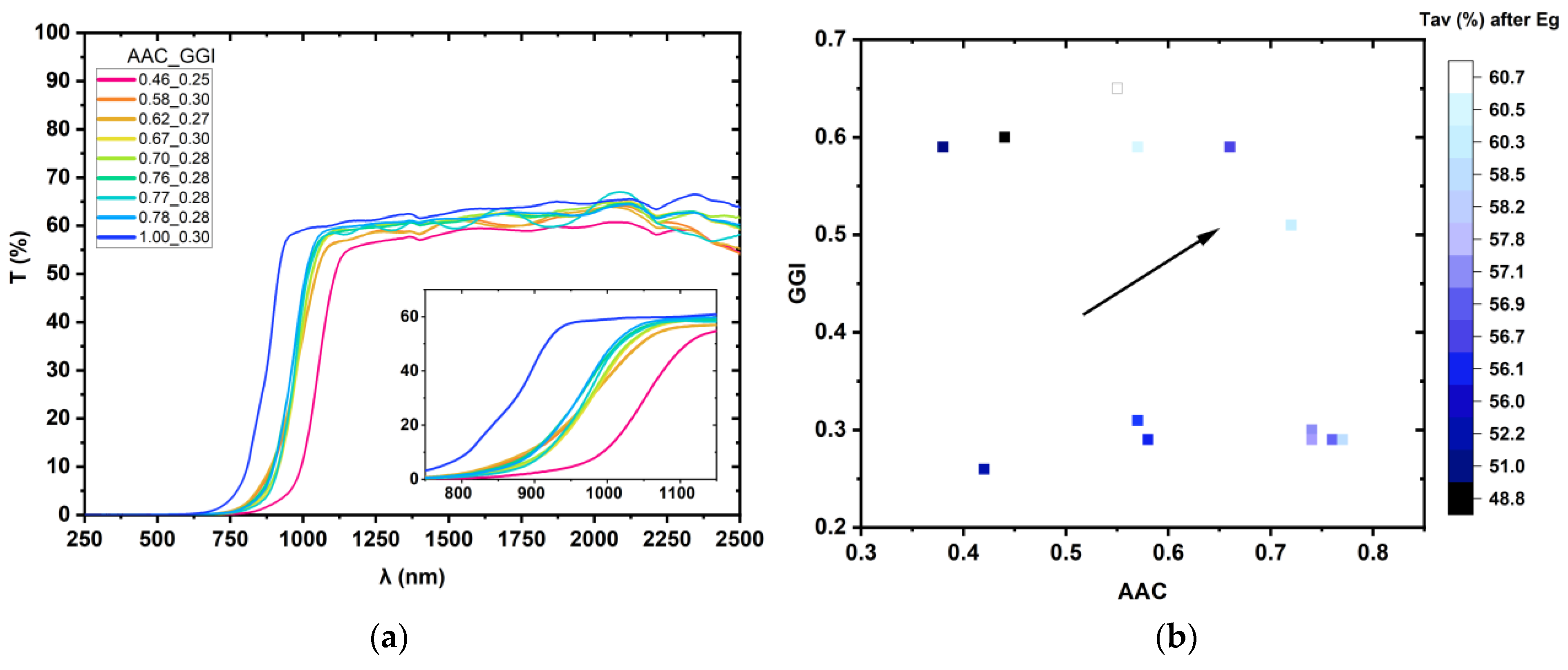
Transmission measurements of the sample series with low Ga content (GGI ratio between 0.25 and 0.30) and AAC varying between 0.46 and 1.00 are shown in Figure 1a. The corresponding data for the series with high Ga content (GGI ratio between 0.50 and 0.59) and AAC between 0.40 and 1.00 is given in the Supplementary Materials Figure S1a. Different groups of compositions can be identified with a similar wavelength where the steep transmission rise occurs (see also the inset). The largest gap wavelength is found for GGI = 0.25 and AAC = 0.46, and the lowest one for GGI = 0.30 and AAC = 1.00, indicating a clear rise in band gap with increasing Ga and Ag content, as will be detailed below. Interestingly, all the other compositions in-between group around a similar gap wavelength, resulting from the highly comparable Ga content and a variation of AAC from 0.58 to 0.78 only. The transmission rise shortly below the gap wavelength is comparably small for all cases, indicating a promisingly low number of states reaching into the band gap. Above the band gap wavelength, the transmission curves stay at a relatively constant level. Furthermore, it can be observed that in some cases clear Fabry-Perot interferences occur, whereas for other samples basically a flat profile is identified. The mostly flat profiles can be related to a high surface roughness of the samples which is also indicated by SEM topographical views and a high diffuse reflection (not shown here).
The average sub-gap transmission Tav was calculated by integration of the transmission from the wavelength of half maximum at the steep transmission rise to the long wavelength end (and accordingly later for reflection). After division by the number of wavelengths included in the integral, an average was obtained, as shown in Figure 1b. The values ranged between approx. 50 and 60%, still leaving room for improvement when thinking about application in, e.g., tandem solar cells. However, it has to be considered that these transmission values were taken for absorbers on glass substrates with a high refractive index contrast of 1 (air) to approx. 2.5 (absorber), resulting in a theoretical reflection of, on average, 25% and an experimentally measured one of approx. 30% (see Figure S1b). The high experimental values can also be correlated with the extremely high diffuse contribution of roughly two-thirds of the reflection values. In the device, including the window layers of CdS, i-ZnO and Al:ZnO, and perhaps even an antireflection coating, these numbers will be significantly reduced. The trend to be noted from Figure 1b is an increase in average sub-gap transmission with increasing Ag content and generally a further benefit of higher Ga ratios (compare the indicative arrow in the figure).
The optical data were utilized for band gap extraction of the various absorbers. Therefore, in the first and preferred case, the transmission curves were linearly fitted in the range of steepest slope and the wavelength values read out for 0% T. Subsequent conversion to the energy delivered the band gap values. An alternative, and the second approach of band gap extraction from transmission and reflection data, is via a Tauc plot of (αhν)² vs. (hν), where α represents the absorption coefficient and (hν) stands for the photon energy. The following equation is used to determine the absorption coefficient [15]
α = 1 d l n ( ( 1 R ) ² T ) ,
where d is the film thickness, and R and T are the recorded reflectance and transmittance, respectively.
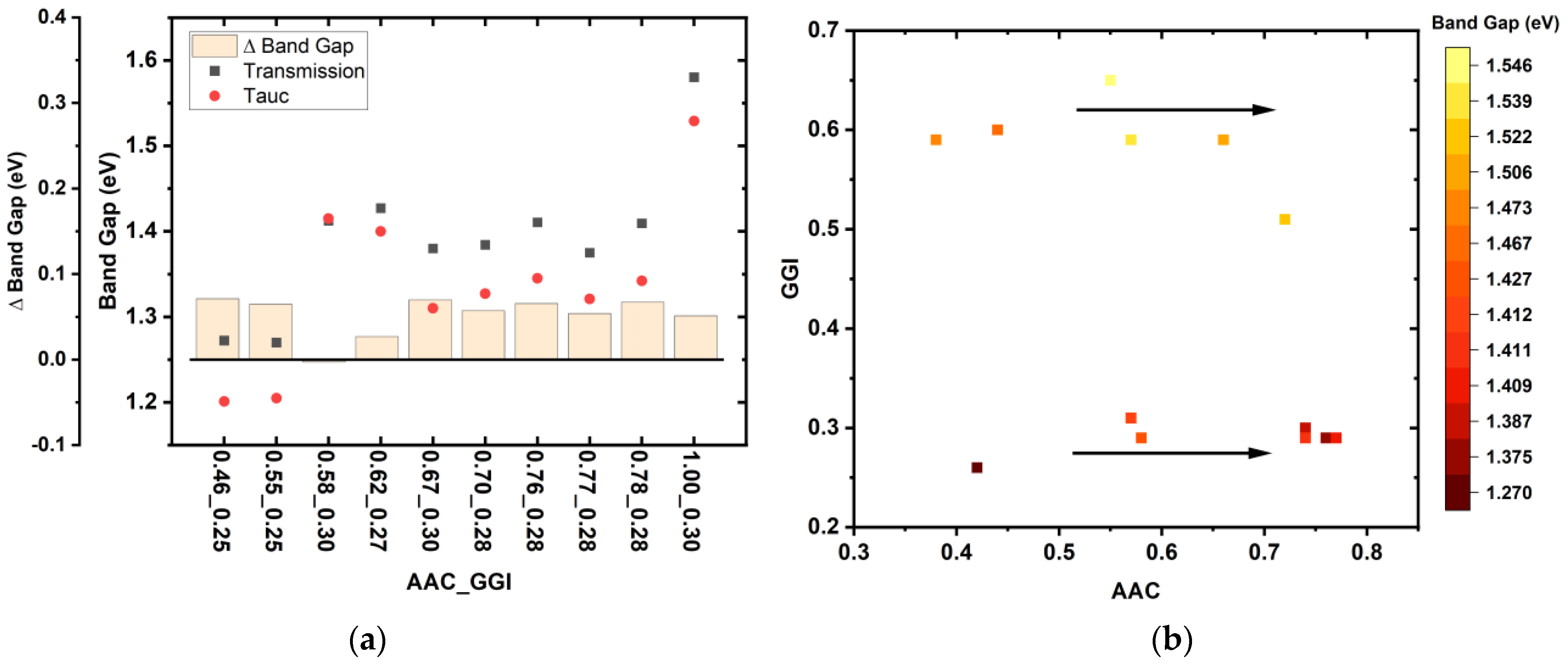
The resulting band gap values and their differences are plotted together in Figure 2a. The two approaches deliver comparable results with approx. 0.050.07 eV higher values for the direct extraction from transmission values. As a constant offset is observed, we favor the first approach of direct slope fitting due to the ease of access and independence of additional parameters (in particular, film thickness). Compared to literature values [10], our band gap numbers are on average 0.1 eV higher for similar compositions, which may be explained by the usage of Tauc plots in the literature references.
An overview of band gap values for our samples is given in Figure 2b as a function of AAC and GGI ratio. Band gap values between 1.27 and 1.55 are found within our composition ranges of AAC between 0.36 and 1.00 and GGI between 0.25 and 0.59. Clear trends of increasing band gap with increasing Ag and increasing Ga content are confirmed as the arrows indicate.

3.2. Raman Spectroscopy

The most common Raman peak of CIGSe is the A1 mode correlated to the vibration of the Se atoms. The A1 mode means that the Se anions are vibrating in the a-b plane and the cations remain fixed [16]. The location of the CIGSe A1 Raman mode is between 173 cm1 (CISe) and 183 cm1 (CGSe) [17]. Another peak around 220 cm1 or above may be correlated to mixed B2/E vibrational modes [18]. Hereby, the B2 mode appears more prominent and relates to the vibration of the cations against the anions in the c-direction [16]. Furthermore, subtle peaks can appear at 150 cm−1, indicating ODCs (ordered defect compounds), or at 260 cm−1, representing the A1 mode of Cu2-xSe [18]. Whereas ODCs are typical for Cu-poor samples, copper selenides occur with Cu-rich compositions.
The investigation of ACIGSe with Raman spectroscopy is less well understood. The Raman peak of ACIGSe is expected to be found between 176 cm1 and 184 cm1 depending on the Ag content (and in the reference, GGI = 0.85) [7]. Generally, it can be noted that the A1 Raman peak shifts to the left (smaller wavenumbers) for larger and to the right (larger wavenumbers) for smaller cations. As Ag has a larger atomic radius than Cu (160 pm as opposed to 135 pm [19]), but In is larger than Ga (155 pm as opposed to 130 pm [19]), the peak shifts to the left with increasing Ag but to the right with increasing Ga content. The higher radii are correlated to larger masses as well as to increased lattice constants, both contributing to smaller Raman shifts [11]. Furthermore, an increasing Cu content (as long as below the stoichiometric ratio of CGI = 1) was correlated to a left shift of the A1 mode, [18] leading to the same expectation for Ag + Cu (AC/IG ratio).
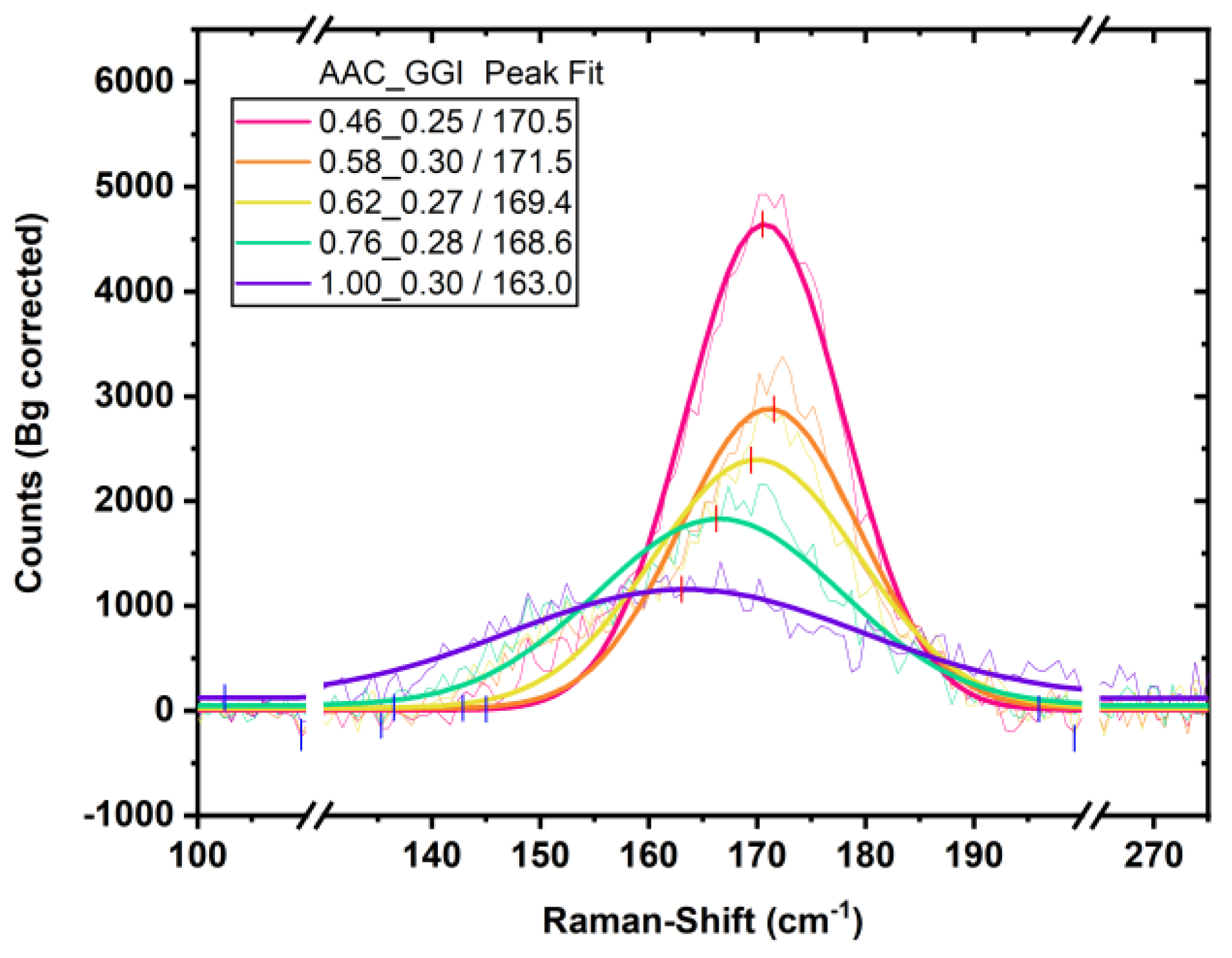
Figure 3 shows the background-corrected and baseline-subtracted main Raman signal of ACIGSe with various Ag contents and GGI around 0.3. The peak values determined by Gaussian fitting are also indicated in the legend. The general trend of decreasing Raman shift with increasing Ag content is clearly confirmed. Here the values lie between 163 cm1 and 171 cm1 as we are looking at low GGI ratios of 0.250.30. At the left side of the main A1 peak, a small shoulder is observed which could be correlated to the existence of an ODC [11]. Corresponding to the left shift of the Raman peak with increasing Ag content, the intensity also decreases. This observation can again be correlated to the larger atomic size of Ag compared to Cu and a resulting distortion in the crystal lattice, which is reflected in a less pronounced Raman signal. The decrease in intensity is also in line with a generally observed larger FWHM (full width at half maximum) of the Raman peaks with increasing AAC (not shown here).
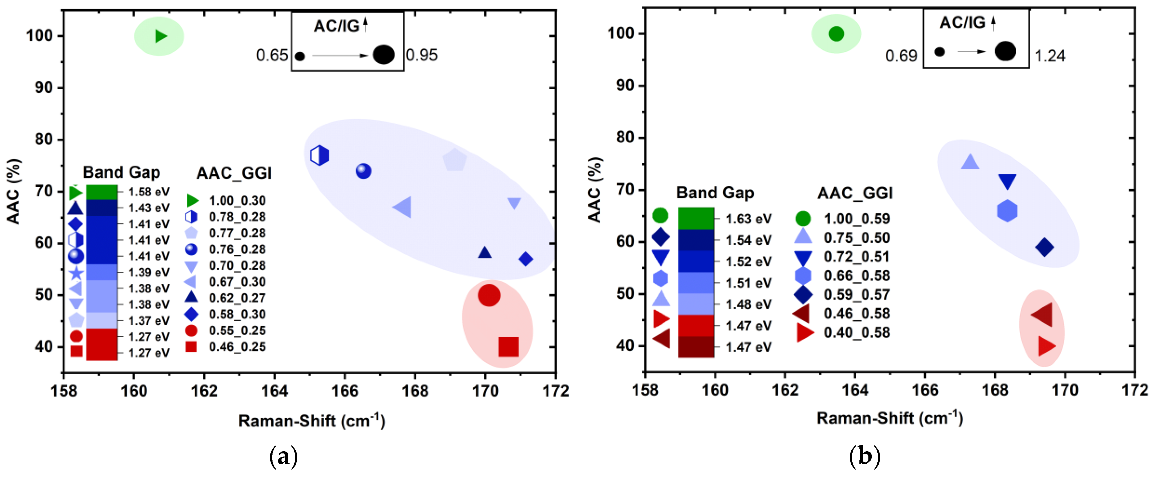
For Figure 3, representative samples were chosen to show the main Raman peak and composition-related trends. The overview of the Raman A1 peak positions for all samples is given in Figure 4. In part (a) the values for low GGI ratios (0.250.30) are presented in dependence of AAC and color-coded by band gap. Accordingly, Figure 4b shows the relations for high GGI ratios (0.500.59). The ratio of AC/IG is also considered in the plots and represented by varying sizes of the symbols. Generally, the trend of decreasing Raman shift with increasing AAC can be confirmed. Furthermore, three groups of band gaps can be separated along with AAC content: 1.27 eV, [1.37,1.43] eV, and 1.58 eV for low GGI and 1.47 eV, [1.48,1.54] eV and 1.63 eV for high GGI. Between the groups, a partial overlap of the Raman peak position occurs. The origin may be found in the difference in AC/IG. Consequently, samples from the red group with AC/IG up to 0.95 or 1.24 (Figure 4a and b, respectively) show similar Raman shifts as samples from the blue group with higher AAC but smaller AC/IG. Also, within the groups of highly similar Ga ratios and hence band gaps, the trend of decreasing Raman shift comes mostly along with increasing AC/IG ratio, which is in agreement with the expectation in the literature. In addition, around the single point of the green group an elliptical area is indicated, giving an idea of variations occurring even for similar compositions and band gaps.
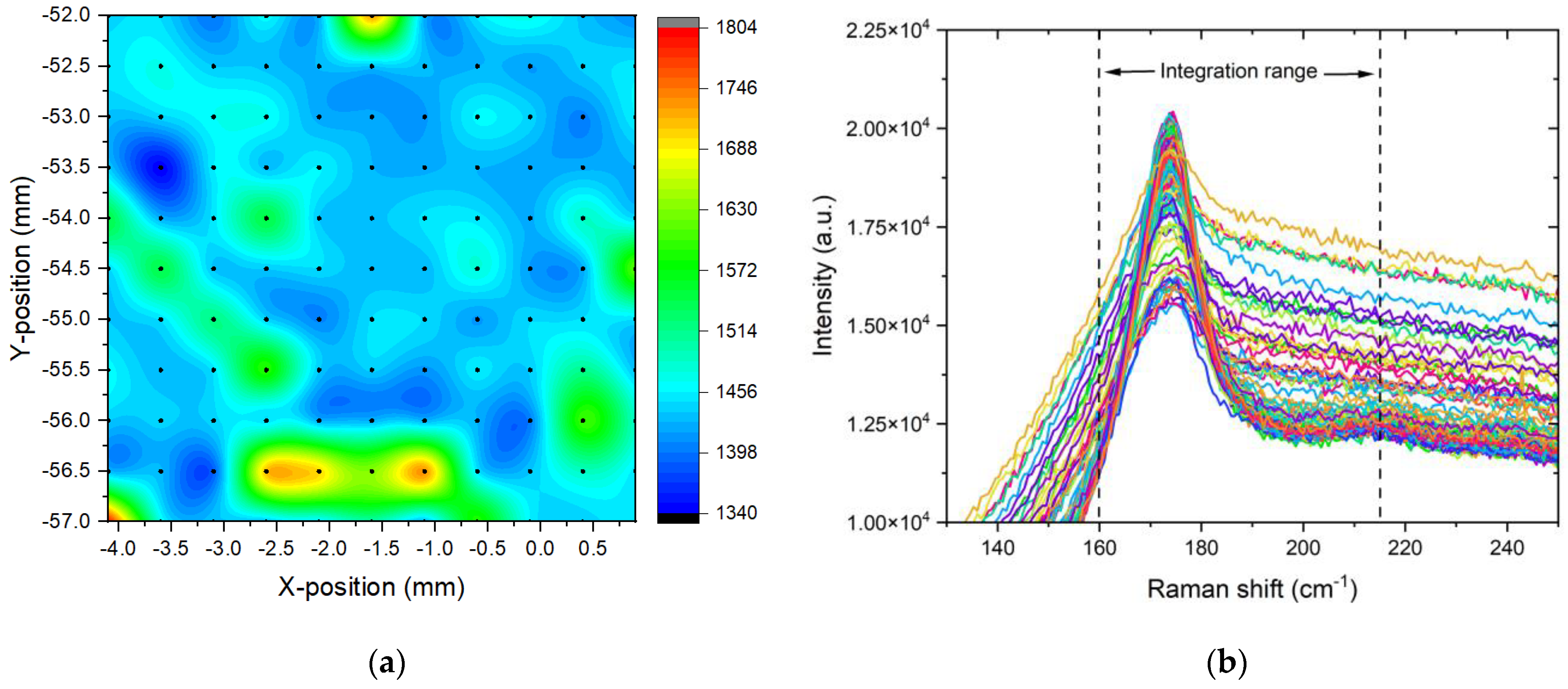
Aside from the expected variation of the Raman signal for different compositions, another variation of the Raman signal across one sample is observed (see Figure 5a). The shown map spans an area of 5 mm x 5 mm with a Raman spectrum recorded every 0.5 mm. The Raman raw signal integrated around the A1 peak in the range of 160–215 cm−1 is mapped. All the corresponding single spectra are shown together in Figure 5b. They reveal changes in intensity and differences in the sharpness of the peaks. At the one end, high-intensity spectra with a broad A1 peak are observed. At the other end, high intensities appear at the A1 peak only, which is characterized by a small FWHM. Additionally, in these cases, a peak shortly below 220 cm−1 is clearly recognized, which can be attributed to the B2 mode. For further illustration, Figure S2 plots the Raman spectra at the maximum and minimum values of Figure 5a only. In the end, the broad high-intensity spectra result in large integrated values (shown in orange and reddish in Figure 5a), whereas the spectra with sharp peaks and small FWHM deliver small integration numbers (bluish in Figure 5a). Therefore, the blue spaces in Figure 5a may be correlated to areas with better crystallinity, and the reddish areas mark lower material quality.

3.3. X-ray Diffraction

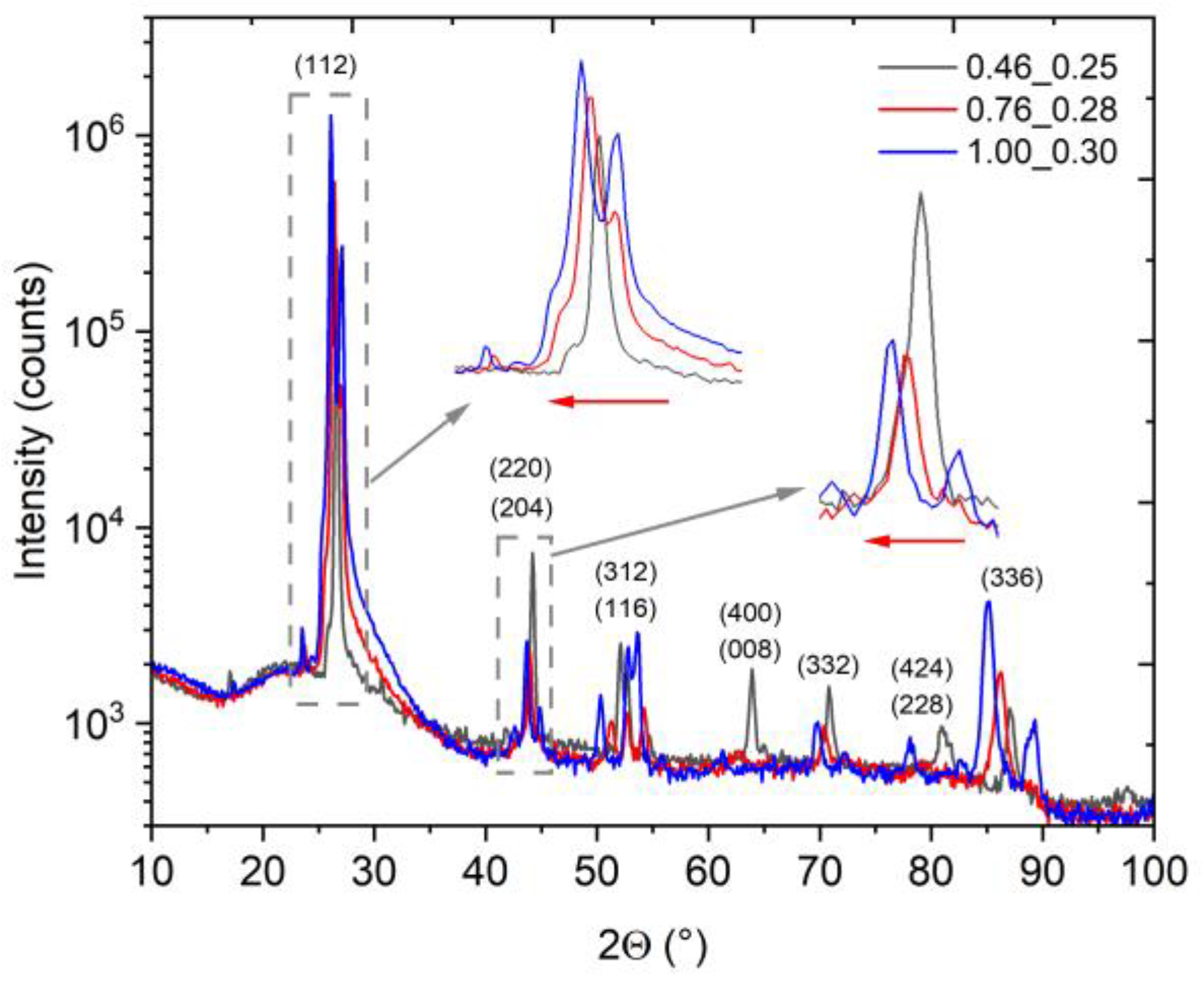
Exemplary XRD spectra of ACIGSe absorbers with varying Ag content (AAC = 0.46, 0.76, and 1.00) and Ga content in a comparably low range (GGI = 0.25, 0.28, and 0.30) are visualized in Figure 6.
The main ACIGSe peak attributed to the (112) orientation is observed around 26–27° and shows a shift to smaller angles with increasing Ag content. In detail, it occurs at 26.6° for the composition of AAC = 0.46 and GGI = 0.25 and shifts to 26.35° for AAC = 0.76 and GGI = 0.28 and to 26.1° for AAC = 1.00 and GGI = 0.30. The left shift of the main peak with increasing Ag content may be related to the larger size of the Ag compared to the Cu atom (see also Raman section) and a related larger lattice constant [20]. According to the Bragg formula, a larger lattice constant results in smaller scattering angles. Furthermore, for larger Ag concentrations (here AAC ≥ 0.76) a secondary peak appears at slightly higher angles than the (112) peak and experiences a shift to larger angles for increasing Ag concentration. This occurrence of a satellite peak was also observed in the literature, but could not be attributed to a certain phase and remained linked to ODCs and related secondary phases only [21].
The peaks at ~42–45°and ~52–54° are attributed to the (220)/(204) and the (312)/(116) orientation, respectively. Like the (112) peak, they reveal a left shift with increasing Ag content as well as the occurrence of a side peak towards the longer angles for higher AAC. The separation of these doublet peaks may be attributed to a distortion of the tetragonal unit cell which apparently becomes more prominent with increasing Ag content [20]. Further peaks at ~64°, ~70–72°, ~78–81°, and ~85–89° may be linked to the ACIGSe (400)/(008), (332), (424)/(228), and (336) orientations. Also, secondary phases become likely to be seen in the more compositionally complex systems.
The increase in the intensity of the main (112) peak along with the decreasing signal of the (220)/(204) doublet for growing Ag content hints at an improved crystal quality with increasing Ag incorporation. The splitting of the peaks, in contrast, remains an indication of lattice distortion compared to the less complex systems. All in all, our XRD spectra are in agreement with literature data as well as with the trends we derived from the optical measurements.

3.4. Current-Voltage Measurements

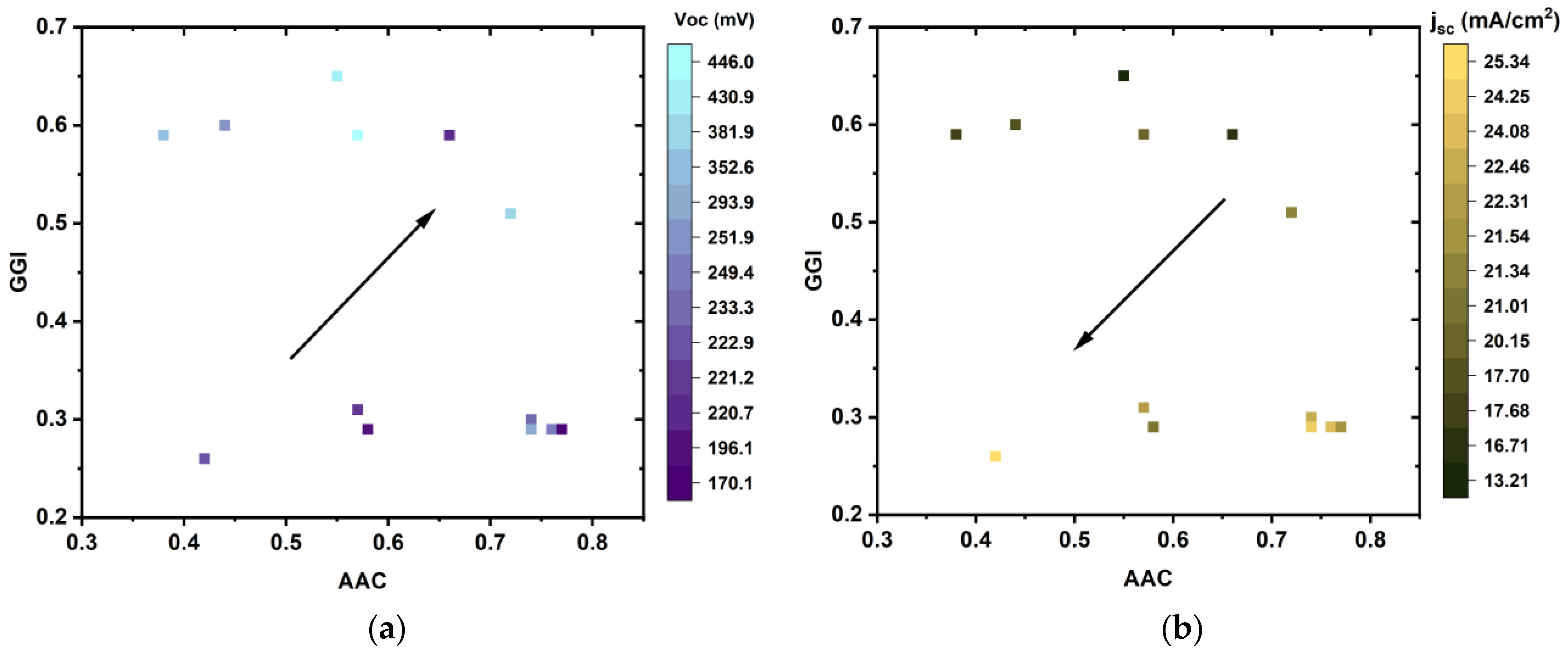
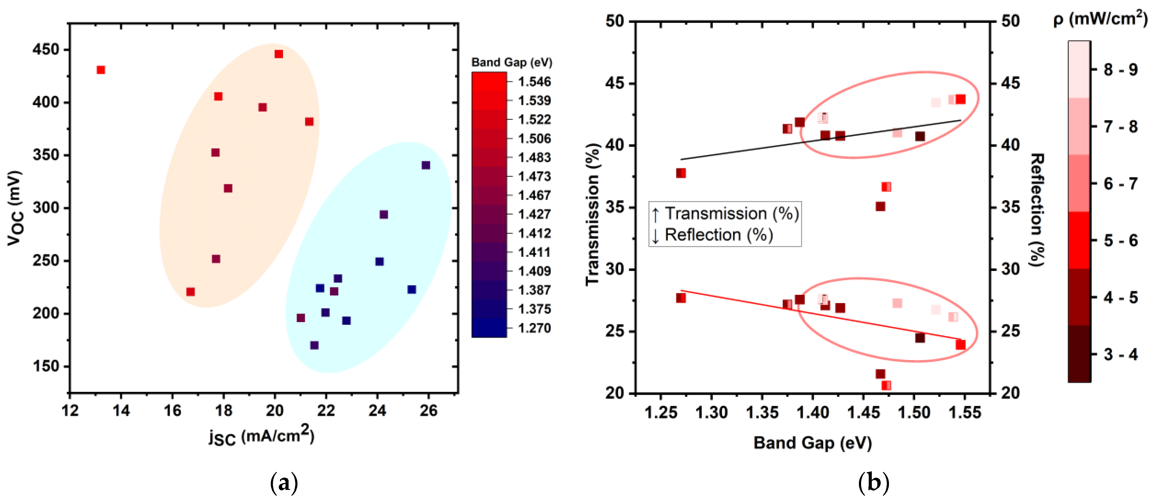
For each composition, one substrate was processed to solar cells and characterized by jV measurements. The resulting open circuit voltage Voc, short circuit current density jsc, and power density ρ values were averaged over all cells, i.e., eight in the ideal case, and accordingly reduced for those with a fill factor below 25%. Voc and jsc as a function of GGI and AAC ratios are presented in Figure 7a,b, respectively. The expected trends of increasing Voc and decreasing jsc with increasing Ag and Ga content can be followed. Voc and jsc are correlated with GGI and AAC via the band gap, for the latter see Figure 2b. In the jsc/Voc landscape depicted in Figure 8a, two groups become visible: samples with band gaps between 1.27 and 1.43 eV and those with Eg between 1.47 and 1.55 eV. The larger band gaps are related to higher Voc and lower jsc, and the smaller ones to lower Voc and higher jsc. The direct correlation is that larger band gaps imply higher energetic photons to be absorbed more efficiently, resulting in a higher Voc, yet overall fewer photons being absorbed, i.e., lower jsc.
Figure 8b shows the power densities achieved in correlation with the transmission and reflection values for the different samples. As was already seen in Figure 1b, larger AAC ratios are correlated with higher sub-gap transparency, which was found to be associated with lowered reflection, in particular for low GGI (see also Figure S1b). As higher AAC ratios are equally linked to a larger band gap, the trend of increasing transmission and reducing reflection with higher band gaps, apparent in Figure 8b, becomes clear. Along with this beneficial improvement in transmission, the achieved power density also rises, proving a clear benefit of the large band gap absorbers for future applications.
4. Conclusions

In summary, we have fabricated ACIGSe absorbers with compositions ranging from 0.36–1.00 for AAC and from 0.25–0.59 for GGI. The related band gaps were extracted from transmission and reflection measurements and resulted in 1.27 eV < Eg < 1.55 eV. The trend of increasing band gap associated with growing Ag and Ga content was confirmed. Sub-gap transparencies ranged between 50 and 60% for the bare absorber, correlated with reflectivities around 30% in the case of high refractive index contrast (to air). In the complete layer stack, this value will be significantly reduced, benefitting the light exploitation by the solar cell structure. Raman measurements on ACIGSe samples with various compositions clearly revealed the A1 peak around 170 cm−1, which is experiencing a shift to lower wavenumbers with increasing Ag and decreasing Ga content. The Raman signals were mapped for different compositions as well as across one sample. Areas of high and low crystal quality may be identified as a result of the sharpness of the Raman peaks. XRD measurements confirmed the crystallinity and revealed reflections according to the various lattice planes as expected from the literature. The peak shifts and occurrence of additional phases with increasing Ag and Ga content could be observed along with the more pronounced existence of the main (112) peak at approx. 26° for higher Ag ratios. Again, this is a confirmation of higher material quality with the integration of Ag into the chalcopyrite compound. Finally, electrical characterization could be brought in line with the observation of increasing band gap for higher Ag and Ga ratios, leading accordingly to higher Voc but lower jsc. A rise in power density along with enhanced sub-gap transmission for the high band gap absorbers shows a promising route for application in semitransparent devices.

Supplementary Materials

The following supporting information can be downloaded at: https://www.mdpi.com/article/10.3390/pr11020392/s1, Figure S1: (a) Transmission curves of ACIGSe with high GGI (approx. 0.5–0.6) and varying AAC ratio; (b) Reflection curves of ACIGSe with low GGI (approx. 0.3) and varying AAC ratio.; Figure S2: Raman spectra recorded at the position of maximum and minimum integrated value according to the map in Figure 5a (dark red and dark blue spot, respectively); the green lines indicate the integration range, the black dashed curve is the minimum curve shifted to fit the peak intensity with the max curve.

Author Contributions

Conceptualization, M.S.; methodology, T.K., I.K. and J.K.; validation, J.K., I.K., T.K., Y.G. and M.S.; formal analysis, J.K., T.K., I.K., Y.G. and M.S.; investigation, J.K., I.K. and T.K.; writing—original draft preparation, M.S.; writing—review and editing, Y.G., I.K., T.K.; visualization, T.K., I.K. and J.K.; supervision, M.S.; project administration, M.S.; funding acquisition, M.S. All authors have read and agreed to the published version of the manuscript.

Funding

The XRF measurements were performed on an instrument funded by the Deutsche Forschungsgemeinschaft (DFG, German Research Foundation)—INST 20876/324-1 FUGG and are acknowledged as follows: “Gefördert durch die Deutsche Forschungsgemeinschaft (DFG)—Projektnummer INST 20876/324-1 FUGG”. The X-ray data were collected using the Rigaku Smartlab High Resolution X-ray diffractometer of the Nanoparticle Processing Technology (NPPT) group at the University Duisburg-Essen. The instrument is funded through the DFG (German Research Foundation) Instrument proposal INST 20876/395-1 FUGG project number 450350889 and the state of North Rhine-Westphalia, Germany. We would like to thank Dr. Martin A. Schroer for assistance in using the instrument. The Raman measurements were performed on a Next-Gen Cluster-Tool funded by the Deutsche Forschungsgemeinschaft (DFG, German Research Foundation)—INST 20876/347-1 FUGG and are acknowledged as follows: “Gefördert durch die Deutsche Forschungsgemeinschaft (DFG)—Projektnummer INST 20876/347-1 FUGG”. We acknowledge T.H. Witte-Nguy for reference setting.

Data Availability Statement

The data are available from the authors upon request.

Conflicts of Interest

The authors declare no conflict of interest.

References

  1. Ramanujam, J.; Singh, U.P. Copper indium gallium selenide based solar cells–A review. Energy Environ. Sci. 2017, 10, 1306–1319. [Google Scholar] [CrossRef]
  2. Nakamura, M.; Yamaguchi, K.; Kimoto, Y.; Yasaki, Y.; Kato, T.; Sugimoto, H. Cd-Free Cu(In,Ga)(Se,S)2 Thin-Film Solar Cell With Record Efficiency of 23.35%. IEEE J. Photovolt. 2019, 9, 1863–1867. [Google Scholar] [CrossRef]
  3. Ishizuka, S.; Nishinaga, J.; Beppu, K.; Maeda, T.; Aoyagi, F.; Wada, T.; Yamada, A.; Chantana, J.; Nishimura, T.; Minemoto, T.; et al. Physical and chemical aspects at the interface and in the bulk of CuInSe2-based thin-film photovoltaics. Phys. Chem. Chem. Phys. 2022, 24, 1262–1285. [Google Scholar] [CrossRef] [PubMed]
  4. Maeda, T.; Nakanishi, R.; Yanagita, M.; Wada, T. Control of electronic structure in Cu(In,Ga)(S,Se)2 for high-efficiency solar cells. Jpn. J. Appl. Phys. 2020, 59, SGGF12. [Google Scholar] [CrossRef]
  5. Sozzi, G.; Menozzi, R. On the effect of deep defects on the Voc deficit in high-GGI CIGS absorbers: A numerical study. In Proceedings of the 47th IEEE Photovoltaic Specialists Conference (PVSC), Virtual Meeting, 15 June–21 August 2020; pp. 0759–0762. [Google Scholar]
  6. Hanket, G.M.; Boyle, J.H.; Shafarman, W.N. Characterization and device performance of (AgCu)(InGa)Se2 absorber layers. In Proceedings of the 34th IEEE Photovoltaic Specialists Conference (PVSC), Philadelphia, PA, USA, 7–12 June 2009; pp. 001240–001245. [Google Scholar]
  7. Keller, J.; Stolt, L.; Sopiha, K.; Larsen, J.; Riekehr, L.; Edoff, M. On the Paramount Role of Absorber Stoichiometry in (Ag,Cu)(In,Ga)Se2 Wide-Gap Solar Cells. Solar RRL 2020, 4, 2000508. [Google Scholar] [CrossRef]
  8. Kim, G.; Kim, W.M.; Park, J.-K.; Kim, D.; Yu, H.; Jeong, J.-H. Thin Ag Precursor Layer-Assisted Co-Evaporation Process for Low-Temperature Growth of Cu(In,Ga)Se2 Thin Film. ACS Appl. Mater. Interfaces 2019, 11, 31923–31933. [Google Scholar] [CrossRef] [PubMed]
  9. Yang, S.-C.; Sastre, J.; Krause, M.; Sun, X.; Hertwig, R.; Ochoa, M.; Tiwari, A.N.; Carron, R. Silver-Promoted High-Performance (Ag,Cu)(In,Ga)Se2 Thin-Film Solar Cells Grown at Very Low Temperature. Solar RRL 2021, 5, 2100108. [Google Scholar] [CrossRef]
  10. Keller, J.; Sopiha, K.V.; Stolt, O.; Stolt, L.; Persson, C.; Scragg, J.J.S.; Törndahl, T.; Edoff, M. Wide-gap (Ag,Cu)(In,Ga)Se2 solar cells with different buffer materials—A path to a better heterojunction. Prog. Photovolt. Res. Appl. 2020, 28, 237–250. [Google Scholar] [CrossRef]
  11. Boyle, J.; Hanket, G.; Shafarman, W. Optical and quantum efficiency analysis of (Ag,Cu)(In,Ga)Se2 absorber layers. In Proceedings of the 34th IEEE Photovoltaic Specialists Conference (PVSC), Philadelphia, PA, USA, 7–12 June 2009; pp. 001349–001354. [Google Scholar]
  12. Richards, M. MiaSolé Achieves Flexible Substrate Thin-Film Solar Cell Efficiency of 20.56 Percent. Available online: https://miasole.com/miasole-achieves-flexible-substrate-thin-film-solar-cell-efficiency-of-20-56-percent/ (accessed on 10 March 2022).
  13. Zhao, Y.; Yuan, S.; Kou, D.; Zhou, Z.; Wang, X.; Xiao, H.; Deng, Y.; Cui, C.; Chang, Q.; Wu, S. High Efficiency CIGS Solar Cells by Bulk Defect Passivation through Ag Substituting Strategy. ACS Appl. Mater. Interfaces 2020, 12, 12717–12726. [Google Scholar] [CrossRef] [PubMed]
  14. Valdes, N.; Lee, J.; Shafarman, W. Comparison of Ag and Ga alloying in low bandgap CuInSe2-based solar cells. Sol. Energy Mater. Sol. Cells 2019, 195, 155–159. [Google Scholar] [CrossRef]
  15. Larsen, J.K.; Donzel-Gargand, O.; Sopiha, K.V.; Keller, J.; Lindgren, K.; Platzer-Björkman, C.; Edoff, M. Investigation of AgGaSe2 as a Wide Gap Solar Cell Absorber. ACS Appl. Energy Mater. 2021, 4, 1805–1814. [Google Scholar] [CrossRef]
  16. Schmid, T.; Schäfer, N.; Levcenko, S.; Rissom, T.; Abou-Ras, D. Orientation-distribution mapping of polycrystalline materials by Raman microspectroscopy. Sci. Rep. 2015, 5, 18410. [Google Scholar] [CrossRef] [Green Version]
  17. Insignares, C. Raman scattering based strategies for assessment of advanced chalcopyrite photovoltaic technologies: Characterisation of electrodeposited Cu(In,Ga)(S,Se)2 solar cells. Ph.D. Thesis, Universidad de Barcelona, Barcelona, Spain, 2015. [Google Scholar]
  18. Witte, W.; Kniese, R.; Powalla, M. Raman investigations of Cu(In,Ga)Se2 thin films with various copper contents. Thin Solid Film. 2008, 517, 867–869. [Google Scholar] [CrossRef]
  19. Slater, J.C. Atomic Radii in Crystals. J. Chem. Phys. 1964, 41, 3199–3204. [Google Scholar] [CrossRef]
  20. Boyle, J.H.; McCandless, B.E.; Shafarman, W.N.; Birkmire, R.W. Structural and optical properties of (Ag,Cu)(In,Ga)Se2 polycrystalline thin film alloys. J. Appl. Phys. 2014, 115, 223504. [Google Scholar] [CrossRef]
  21. Simchi, H.; McCandless, B.; Shafarman, W.; Kim, K.; Boyle, J.; Birkmire, R. Surface characterization of (AgCu)(InGa)Se2 thin films for solar cells. In Proceedings of the 37th IEEE Photovoltaic Specialists Conference, Seattle, WA, USA, 19–24 June 2011; pp. 000041–000045. [Google Scholar]
Figure 1. (a) Transmission curves of ACIGSe with low GGI (approx. 0.3) and varying AAC ratio; (b) Average sub-gap transmission values as a function of GGI and AAC (arrow indicating increasing trend).
Processes 11 00392 g001
Figure 2. (a) Band gap of ACIGSe with various compositions obtained by linear fitting of the steep rise in transmission curves, or a Tauc plot of (αhν)² vs. (hν) along with the difference between the values; (b) Band gap values as a function of AAC and GGI ratios derived from slope fitting of transmission curves (arrows indicating increasing trend).
Processes 11 00392 g002
Figure 3. Raman signal of main A1 mode for ACIGSe of different compositions as indicated. The fitted peak value in cm1 is also given.
Processes 11 00392 g003
Figure 4. Raman shift of ACIGSe A1 mode related with AAC ratio, AC/IG ratio (symbol size), and band gap values (color code) for (a) low (0.25–0.30) and (b) high (0.50–0.59) GGI ratios.
Processes 11 00392 g004
Figure 5. (a) Spatial distribution of Raman-shift for exemplary ACIGSe sample; (b) Individual Raman spectra integrated within the given wavenumber range to obtain the map in (a).
Processes 11 00392 g005
Figure 6. XRD spectra for three samples of ACIGSe with different AAC and similar GGI ratio, as indicated in the legend. For the main peaks, zoom-in pictures are given following the grey arrows; the red arrows indicate the shift of the main peak with increasing Ag content.
Processes 11 00392 g006
Figure 7. (a) Open circuit voltage Voc, and (b) short circuit current density jsc of ACIGSe solar cells as a function of GGI and AAC ratios (arrows indicating increasing trends).
Processes 11 00392 g007
Figure 8. (a) Correlation of jsc and Voc with Eg grouped in low (Eg from 1.27 to 1.43 eV, bluish) and high (Eg from 1.477 to 1.55 eV, reddish) values; (b) Power density of ACIGSe solar cells along with the evolution of transmission and reflection depending on the band gap.
Processes 11 00392 g008
Disclaimer/Publisher’s Note: The statements, opinions and data contained in all publications are solely those of the individual author(s) and contributor(s) and not of MDPI and/or the editor(s). MDPI and/or the editor(s) disclaim responsibility for any injury to people or property resulting from any ideas, methods, instructions or products referred to in the content.