Article

Design and Implementation of Active Clamp Flyback Converter for High-Power Applications

1
Key Laboratory of Low-Grade Energy Utilization Technologies and Systems, MOE, Chongqing University, Chongqing 400030, China
2
Department of Electrical and Electronics Engineering, Manipal Institute of Technology, Manipal Academy of Higher Education, Manipal 576104, India
3
Department of Electrical and Electronics Engineering, School of Engineering and Technology, CHRIST (Deemed to Be University), Bangalore 560074, India
4
Department of Electrical and Electronics Engineering, Lakireddy Bali Reddy College of Engineering (Autonomous), Jawaharlal Nehru Technological University, Kakinada (JNTUK), Kakinada 533003, India
5
Department of Electrical and Electronics Engineering, R.V.R & J.C. College of Engineering, Guntur 522019, India
*
Author to whom correspondence should be addressed.
Processes 2023, 11(10), 2980; https://doi.org/10.3390/pr11102980
Submission received: 24 July 2023 / Revised: 9 September 2023 / Accepted: 21 September 2023 / Published: 14 October 2023

Abstract

:
This paper proposes a solar-powered isolated DC–DC converter for high-power applications. The main aim of this paper is to achieve voltage regulation in the output side of the converter and to integrate a lossless active clamp flyback circuit (LACF) to compensate for the high-voltage issues that arise from one-stage DC–DC converters. Hardware is developed with a power rating of 2 kW to test the performance of the proposed circuit. The circuit is designed using low-voltage devices and features such as soft switching and regeneration due to the LACF, which enhances efficiency. A novel luminous control algorithm is presented to improve the converter performance. The proposed circuit’s performance and feasibility are compared with existing converter parameters, such as the number of components in the circuit, voltage rating, and regeneration.

1. Introduction

DC supplies are crucial in domestic electrical systems because domestic appliances demand high-voltage DC rather than AC supplies [1]. However, the efficiency of a system is affected by the multiple stages of power conversion. Hence, it is essential to reduce the number of conversion stages to one in order to achieve higher efficiency [2]. Power generation from renewable energies such as wind and solar power is preferable due to environmental concerns and energy security. Solar energy is produced in the form of DC power, which is a more suitable source for DC appliances used in combination with isolated DC–DC converters [3].
Various DC–DC converter topologies are used to control input voltage according to application requirements. The traditional unidirectional buck and boost converter is the ancestor of the buck–boost bi-directional DC–DC converter. However, these conventional converters operate with a high-duty cycle which results in issues including severe diode reverse recovery, high voltage strains on switches, and low efficiency [4]. Many different high step-up DC–DC converters, such as cascaded DC–DC converters, switched capacitor-based converters, and the coupled inductor-based converter, were later developed to overcome the restrictions imposed by severe duty cycles. These high step-up DC–DC converters, which use linked inductors and voltage multiplier cells, are described in detail and compared in [5]. Furthermore, multilevel converters have been implemented for different high-power applications to enhance voltage gain and conversion efficiency. Nonetheless, the implemented DC–DC converter should possess greater extent feasibility, high efficiency, and a minimal component count in the various applications [6].
Moreover, existing AC–DC converters are used for power factor correction if the source is AC, with a further DC converter stage connected to the output side [7]. This type of conversion system has two conversion stages with drawbacks such as low efficiency, low power density, and a greater component count for circuit operation and control. These drawbacks can be overcome by integrating a lossless active clamp combined with a flyback circuit (LACF) to compensate for high-voltage issues arising from one-stage DC–DC converters [8]. Many one-stage converters, such as flyback, dual-active bridge, and diode-based DC–DC converters, have been presented [9,10,11,12]. A flyback-isolated AC–DC converter has a rectifier with a DC–DC conversion stage [13,14]. DC–DC conversion requires higher current rating switches with different switching frequencies due to the input side AC [15,16,17]. A dual-active bridge converter needs high-frequency input from a regular AC frequency. The alternating current voltage is first converted to direct current through a rectifier circuit [18,19]. This conversion method is compatible with some continuous conversion operations [20,21]. A conversion circuit with open-loop operation has been developed [22,23], although it has some disadvantages, such as control circuit issues and a high switching device count [24,25]. Furthermore, a single-stage diode-based DC–DC converter has a reduced switch count when compared with a dual-active bridge converter, but soft switching operation is difficult in a wide range of operations.
Therefore, LC components are added to achieve smooth operation in various converters proposed for soft switching [26,27,28,29]. These proposed converters with single-stage operation enhance the overall performance, but the input side components are affected by high voltage stress. This problem is overcome by a clamping circuit connected to the input side of the converter. Moreover, a clamp circuit can be of two types, active or passive, and generally a passive clamp circuit requires a resistor, a capacitor, and a diode. The passive clamping circuit is connected to the input side of a high-frequency transformer and the capacitor discharges via a diode within the circuit. If the circuit consists of a resistor, then the stored energy cannot be utilized because of power dissipation, which leads to reduced system efficiency. Therefore, among the two types of circuits, an active clamp-based circuit with some additional devices to enhance circuit efficiency is more advantageous.
A novel flyback converter for renewable energy conversion-based high-power applications has been developed [30,31,32,33]. Zhang et al. [34] discussed interleaved flyback micro converters for photovoltaic (PV) applications. Later, Hu et al. [35] and Kim et al. [36] presented a three-port flyback converter and modified interleaved flyback converter topologies for PV applications, respectively. Furthermore, Sathiya et al. [37] proposed a single-switch integrated boost and flyback converter for sustainable applications. The above topologies are focused on the enhancement of the system’s efficiency, but they suffer from the drawbacks of high conduction losses and low voltage gain. To overcome these limitations, an active clamp flyback converter was discussed in [38]. In addition, Arshak et al. [39] proposed a flyback topology for high-frequency applications. This topology is used to enhance the system’s efficiency with various operating frequencies. The major limitations of the topology are high switching losses and bulkiness. Subsequently, Goudarzian et al. [40] proposed a modified flyback converter for fuel cell applications. The high voltage stress exerted on the components is, however, a drawback.
Existing types of multilevel DC–DC converters, such as non-isolated multiphase converters, flying capacitors, and neutral point clamps, are well established [32]. Nevertheless, the industry prefers non-isolated multiphase topologies due to their superior characteristics. Converters such as the cascaded H-bridge and switched converters have been extensively studied. Non-isolated multiphase DC–DC link converters with a reduced number of switches have been developed for two-stage processes in different high-power applications. These non-isolated multiphase converters, which have a DC source and a control unit, produce many voltage levels across the converter. Moreover, a non-isolated multilevel converter can be used in place of the normal DC–DC converter, which is an extension of traditional topologies [37,38]. This new configuration has recently been used to exploit the non-isolated multiphase DC–DC converter, and it continues to be investigated. However, the major limitation of the topology is the high number of switching components. To overcome this disadvantage, a modified converter with a reduced switch count and a switched ladder-type circuit was developed, but this topology is limited by its low voltage gain and greater number of DC sources, which lead to reduced system efficiency.
Therefore, this paper proposes an isolated DC–DC converter with one conversion stage which is suitable for DC power applications and overcomes the issues related to voltage stress. Moreover, the proposed circuit reuses the stored capacitor energy to direct the current capacitor in every cycle. It also has the advantage of a lower THD (total harmonic distortion), due to the absence of freewheeling, and high conversion efficiency. Furthermore, a novel luminous control algorithm is presented to enhance the converter’s operational performance by controlling the duty cycle. The system is tested by constructing a prototype model with a power rating of 2 kW using an IGBT (insulated gate bipolar transistor). The experimental results under steady state as well as dynamic conditions are presented in Section 4, along with a comparative analysis.

2. Materials and Methods

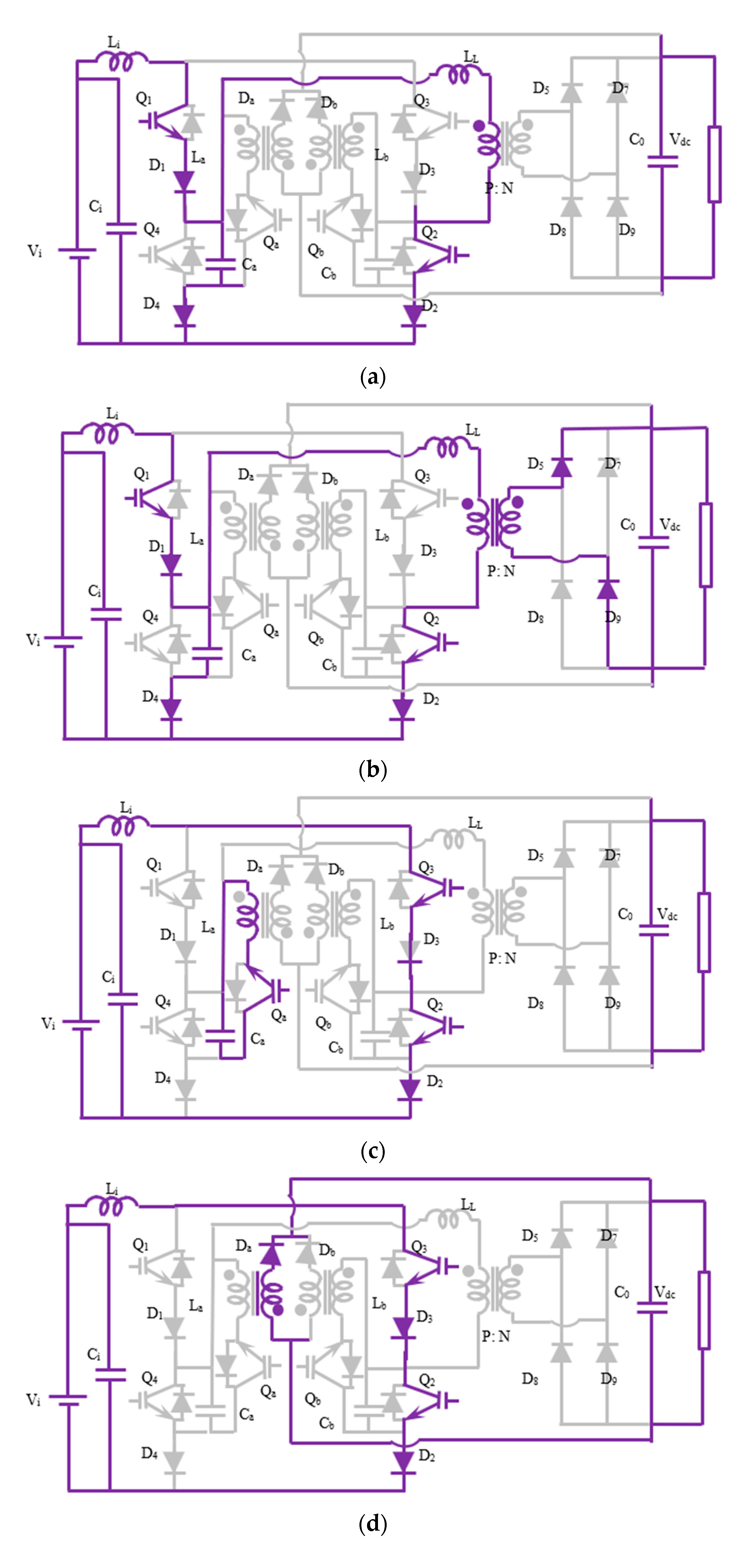
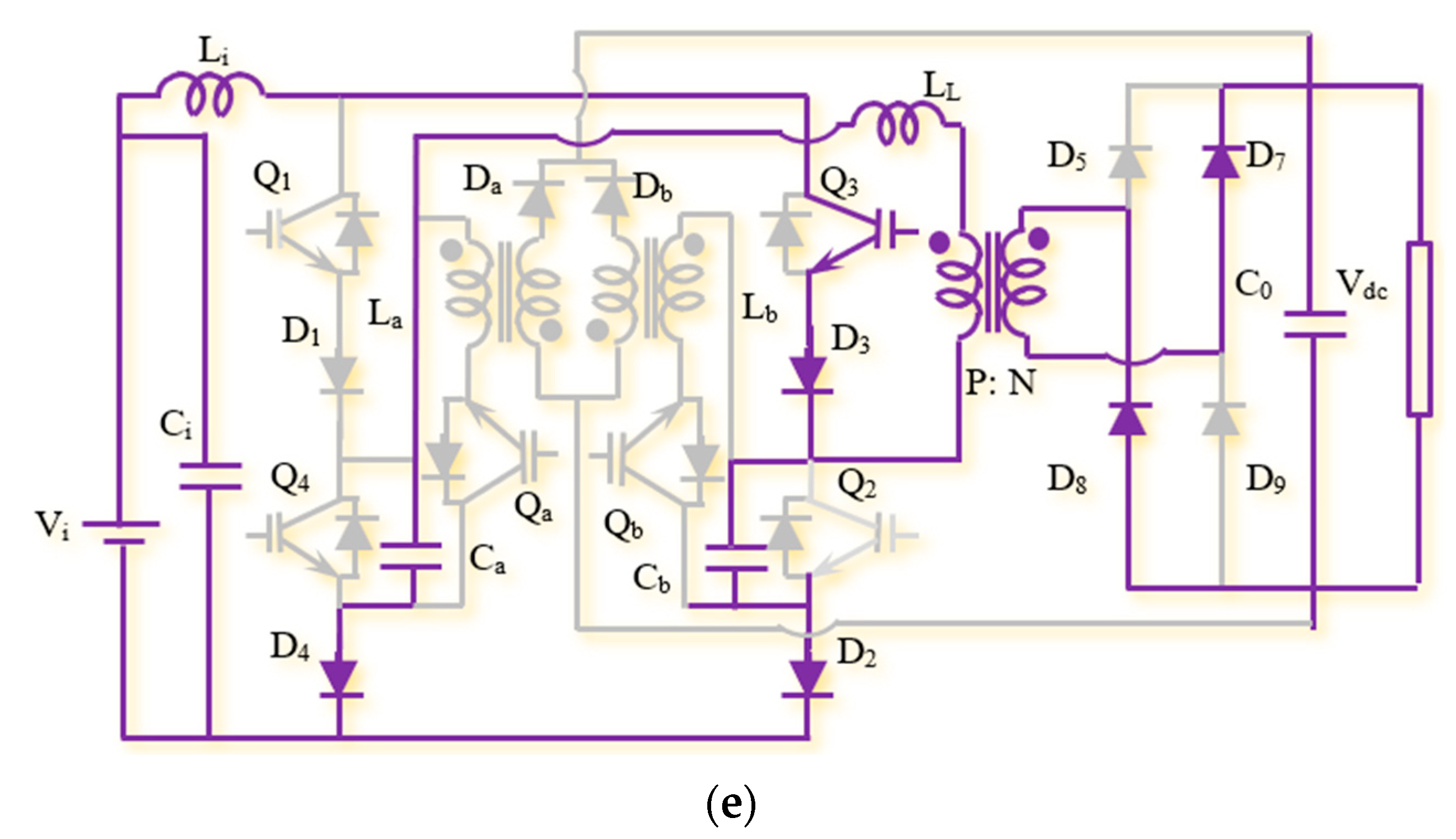
2.1. Proposed Converter

The proposed converter is shown in Figure 1. The circuit consists of 6 IGBTs, whereas the existing converter has 10 IGBTs [18,25]. The following procedure is considered during modes of operation: (i) all IGBTs are ideal, and internal capacitance between the gate and the emitter of switches Q1 to Q4 is denoted by C1 to C4l; (ii) the capacitors in the clamp circuits Ca and Cb are larger than circuit capacitors C2 and C4; (iii) the leakage inductor (LL) energy of the high-frequency transformer is higher than the energy stored in capacitors C1 and C3. The overall converter operation is divided into five modes, which are illustrated in Figure 2a–e.
First mode (t1 to t2): In the time duration t0 to t1, switches Q1, Q2, and Q4 are turned ON and the remaining switches remain in the OFF state. An input current (i1) circulates through switches Q1, D1, Q4, and D4. Clamping capacitors Ca and Cb charge linearly, decreasing to zero. At t = t1, switch Q4 is turned OFF and Q2 and Q4 remain in the ON state. Thus, capacitors Ca and Cb again charge linearly via switch Q4. The circuit will attain peak charging current when Ca > Cb. When switch Q2 is turned OFF, current i1 will linearly decrease to zero via inductor LL without any disturbance, as is illustrated in Figure 2a.
When DC side diodes D5 and D6 are in forward-biased mode, Ca charges from voltage level zero to Vdc, as is illustrated in Figure 2b. The voltages of the various capacitors are given by Equation (1):
V C t = V i t d V i ( t ) d t L i
Second mode (t2 to t3): At the beginning of the second mode, capacitor C3 will charge up to Vdc. At time t2, switch Q3 will turn ON, as is shown in Figure 2b. The inductor LL current decreases for a changing switching operation, i.e., switch Q3 will turn OFF. Again, due to zero-current switching (ZCS), switch Q3 is turned ON. The selection of inductor LL will ensure operation as above. The resonating current from ZCS is given by Equation (2), the current flowing through the inductor is given by Equation (3), and the input side transient voltage across the switch is given by Equation (4):
i C p + C p ( t ) = w r e s w g 2 w r e s 2 I i ( w g w r e s t w r e s w g t ) 2
i p ( t ) = I i [ 1 1 w k 2 1 ( w k sin w r e s t sin w g t ) ]
V d t = n V d + w r e s 2 w g 2 w r e s 2 L l I i w k [ cos w r e s t cos w g t ]
in which iCp is the capacitor peak current, rres is the resistance in the resonant condition, and ωg and ωres are the angular frequencies. Once current Ii is transferred via switch Q3, diodes D1, D5, and D6 will become reverse biased. Subsequently, capacitor Ca will charge up to Vdc.
Third mode (t3 to t4): The circuit diagram for mode 3 operation is given in Figure 2c. When switch Q1 is turned OFF during ZCS, a recycling process will take place such that the energy stored in capacitor Ca will discharge and switch Qa will turn ON immediately. This forms a resonance circuit between the component’s inductor La and Cp. The resonance frequency ωres is given by Equation (5) and the impedance Zres is given by Equation (6):
ω r e s = 1 L a ( C a + C 1 )
Z r e s = j ω r e s L a 1 ω r e s L a ( C a + C 1 )
The energy stored in capacitor Ca flows through inductor La during one quarter of the total resonance period. The duty ratio of switch Qa is given by Equation (7):
D a = t 4 t 3 T s = π L a C a 2 T s
in which Ts is the total switching period. The resonance current of inductor La is given by Equation (8). In the clamping circuit, clamped capacitor Ca will adjust its power factor value, as is illustrated in Figure 2c.
I a = C a L a n V d c sin ( ω r e s D a T s )
Fourth mode (t4 to t5): The energy recycling process resumes in mode 4. Switch Sa is OFF at time t3. Diode Da is illustrated in Figure 2d. Inductor La stores energy, which is circulated back to the capacitor DC bus, completing the recycling process. The proposed circuit recycling takes place twice due to the discharging of capacitors Ca and Cb. The clamping circuit is identical, and the circulated energy in the nth cycle is given by Equation (9):
E r e s = 1 2 L L I a 2
for the nth cycle, in which Eres is the energy from regeneration. During regeneration, and also during ZCS and ZVS conditions, switch Q4 will remain in the ON state. The total power can be calculated using Equation (10), in which ωg is the grid frequency, and Tg is the time duration when the grid supply is connected with the circuit.
P = ω g 2 π n = 0 T g / 2 T s L a ( I a ) 2 n
Fifth mode (t5 to t6): Before the fifth mode, current (ii) circulates through Q3, D3, Q2, and D2. Clamping capacitors Ca and Cb discharge completely. At time t5, switch Q2 is turned OFF from the control. The converter configuration will charge clamping capacitor Cb without creating any disturbance in current ii. Switch Q4 is then turned OFF, and diode D4 will be reverse biased from the operation of inductor LL. The fifth mode of operation is illustrated in Figure 2e. Diodes D7 and D8 are in the conduction state, and clamping capacitor Cb is charging up to Vdc. The fifth mode starts in the second half of the switching duration, from 0 to Ts. The working principle during modes 6 to 8 is the same as that during modes 2 to 4.

2.2. Guidelines for Designing the Clamping Circuit

The working principle of the clamping circuit is the same as that of a resonance series circuit. Clamping capacitors Ca and Cb make the switching operation between the current flow’s inductors Li and LL smooth in both the ON and OFF state. The responses of clamping capacitors Ca and Cb are obtained using Equation (11):
C a , b L L ( I i ,   m a x ) 2 π D a 2
The energy stored in clamping capacitors Ca and Cb will be transferred to inductors La and Lb during one quarter of the resonance time period Ts, beginning from switches Qa and Qb in the ON state, according to Equation (3). The magnetizing inductor value satisfies Equation (12), in which La,b denotes inductance La or Lb:
L a ,   b 4 ( D a T s ) 2 π C a , b
The maximum power point tracking (MPPT) methodology is an effective process for extracting the maximum power from the solar panels, and it is illustrated in the flowchart in Figure 3b. The steps to process the optimal luminous intensity algorithm are as follows:
  • Macrocell solar irradiance from all cells and backup source voltage.
  • Luminous intensity increases the optimal configuration of the photovoltaic arrays.
  • Calculate current from MPPT based on light value.
  • Using the bound and branch method, derive charger voltages in input and output sides.
  • If not, repeat this range for each n, or else end.
  • Find best matches of results in both input and output voltages from battery charger (DC–DC converter).
  • If not, calculate input current and voltage as well as the output voltage of the charger (DC–DC converter), or else end.
  • If not, find optimal n corresponding to m value, or else end.
  • Find and return the optimal n value.
According to the flowchart, certain rules are defined to access the solar panels in the system. In this paper, a voltage of 100 ms is considered for defining the connection of the solar panels to the system. If the solar voltage is lower than the threshold voltage, the solar panels are removed, but otherwise they are included. If the solar voltage is less than or equal to the change in voltage then the solar panel is connected in shunt mode, but otherwise it is in individual mode. Based on the solar input, the total operation is divided into five modes, and switching intervals are shown in Figure 3a.
The power obtained by recycling the energy over the power cycle is given by Equation (13):
P C = ω g 2 π n = 0 T g / 2 T s L a [ C a L a n V d c sin ( ω r e s D a T s ) ] 2
The switching waveforms for all modes of operation are shown in Figure 3a. The final power equation is derived from Equation (9) and is given in Equation (14) below:
P C = C a ( n V d c ) 2 C b ,   π T s

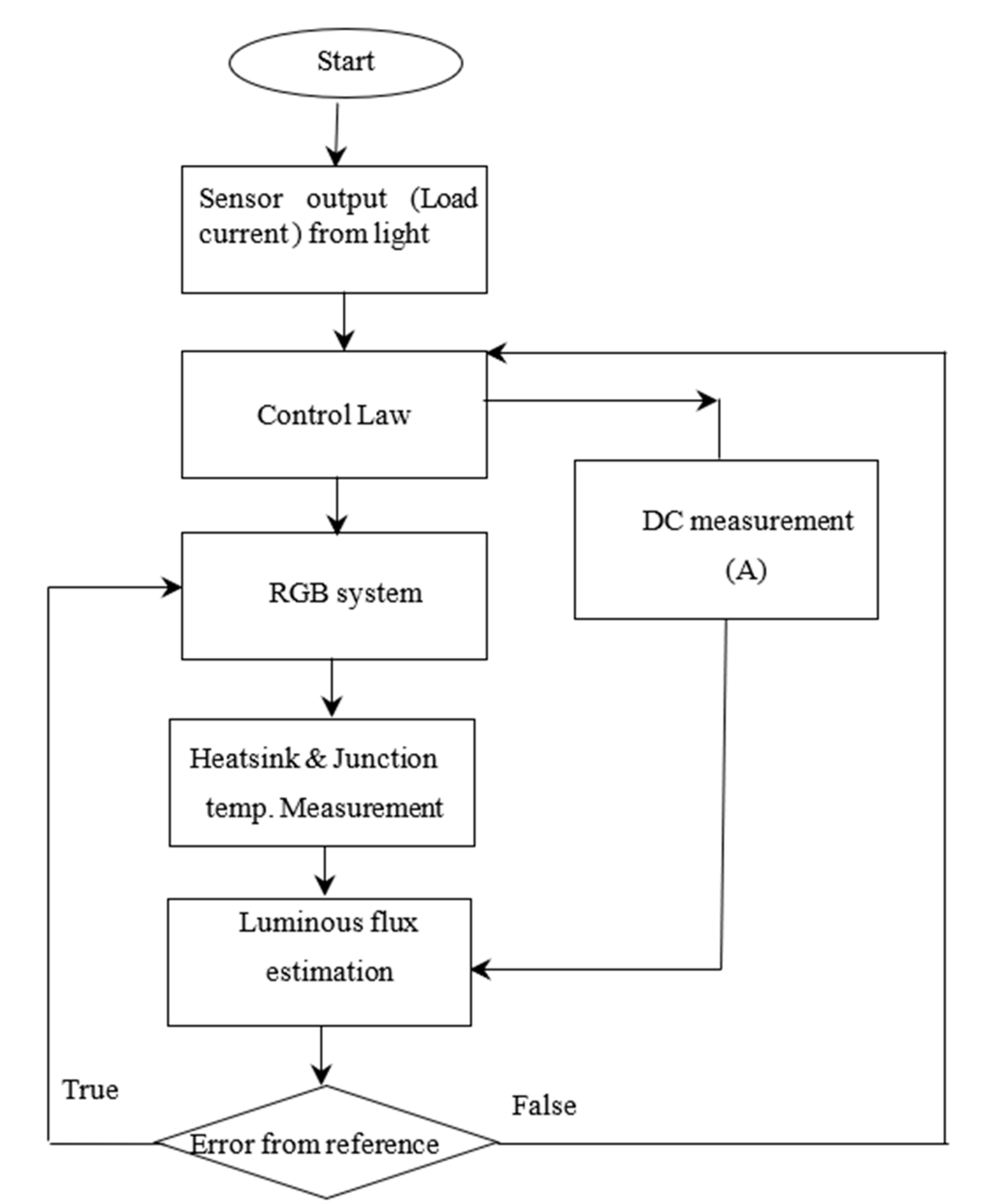
2.3. Luminous Control Algorithm
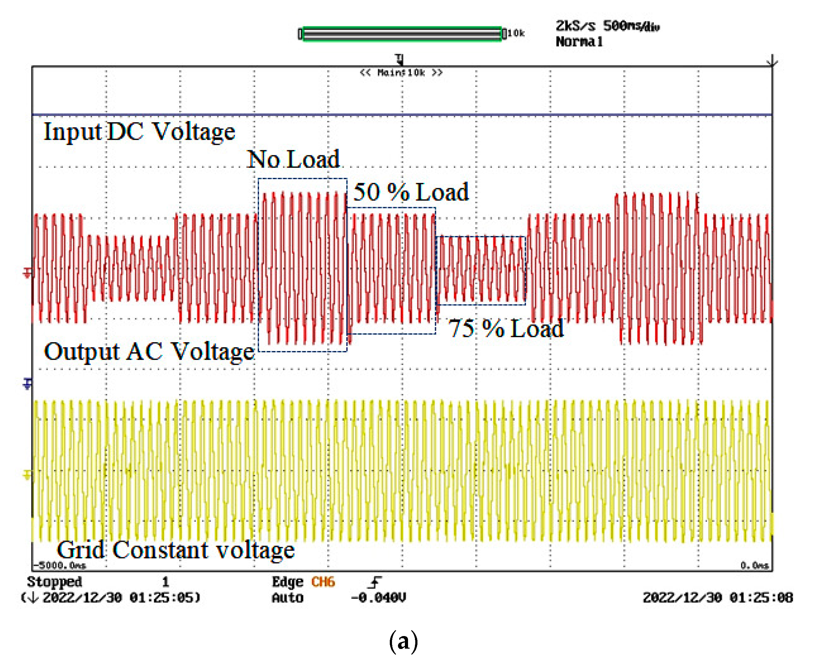
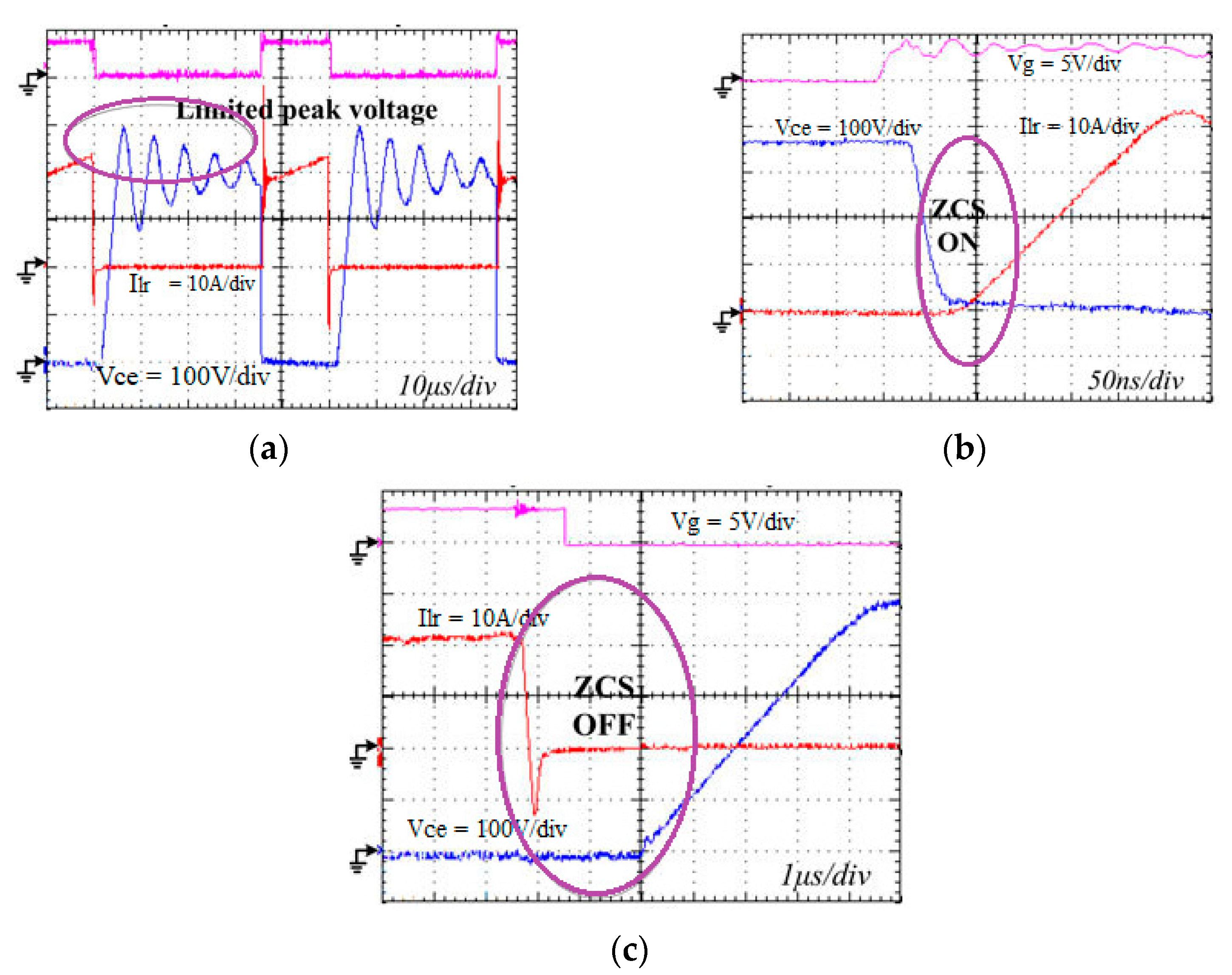
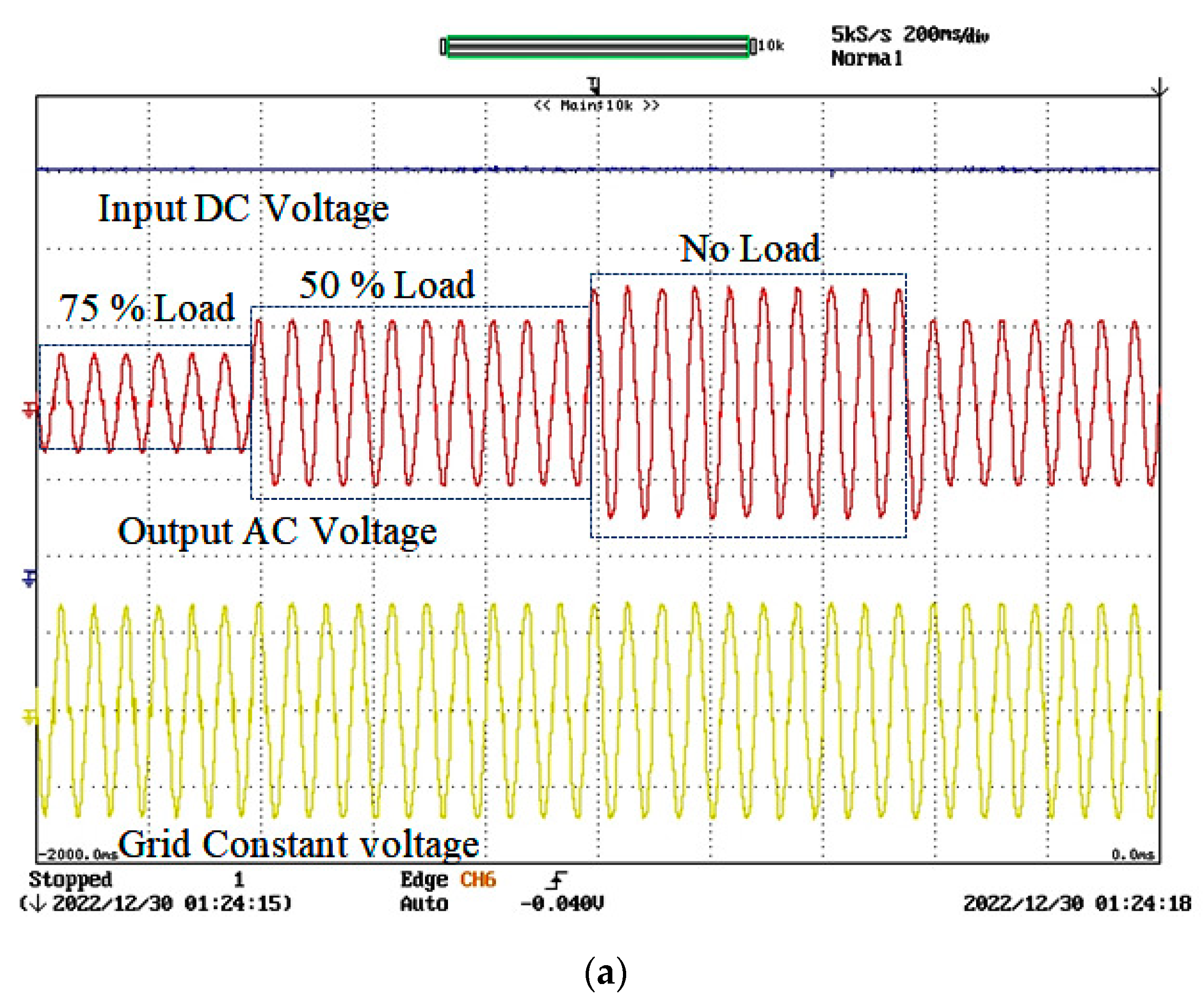
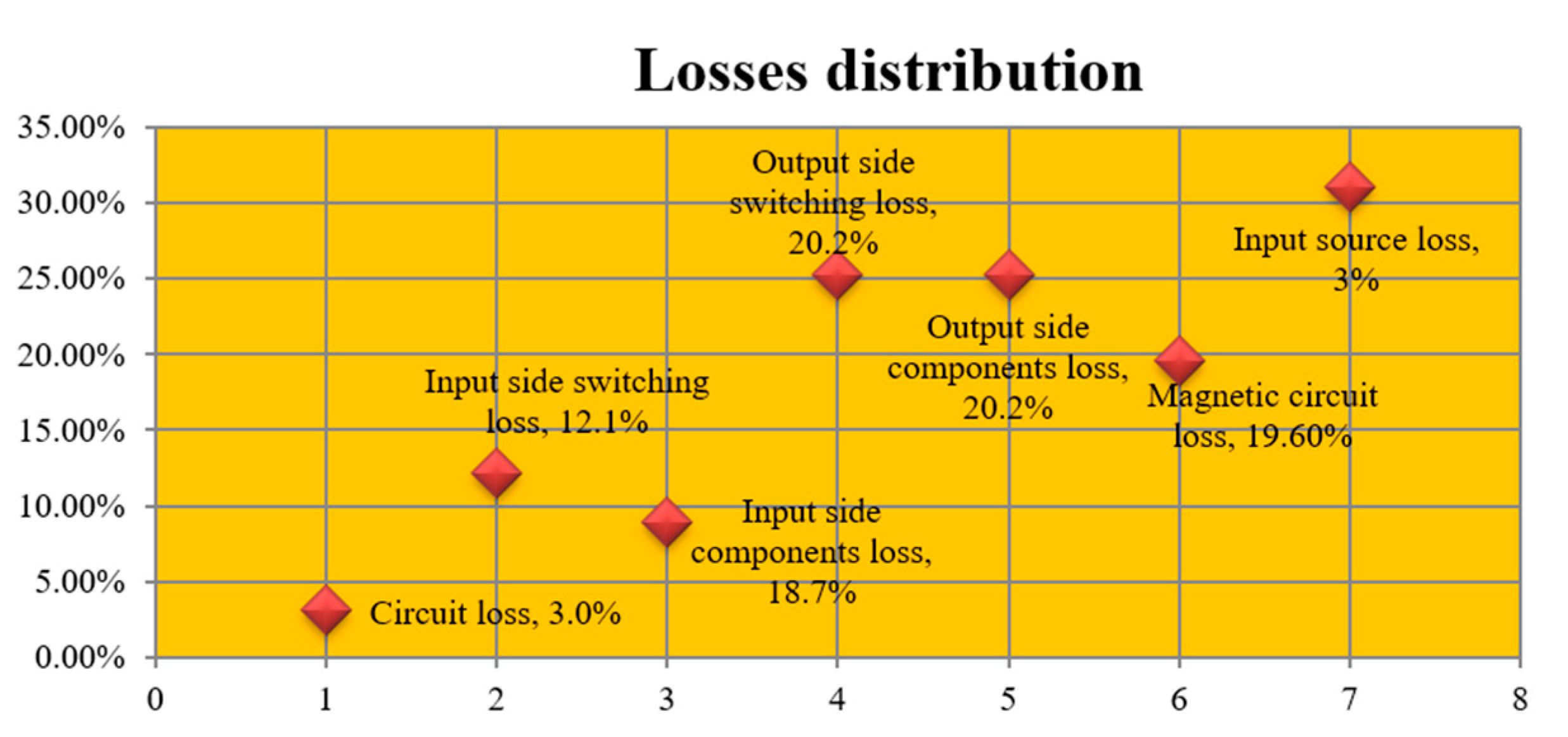
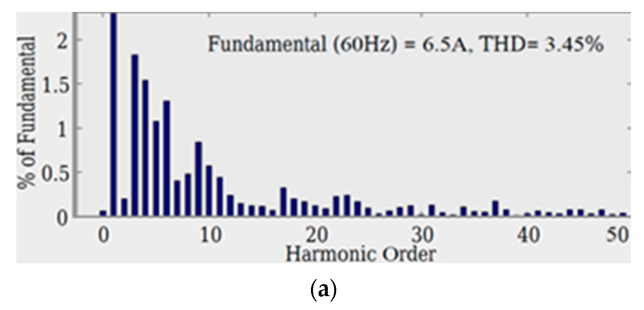
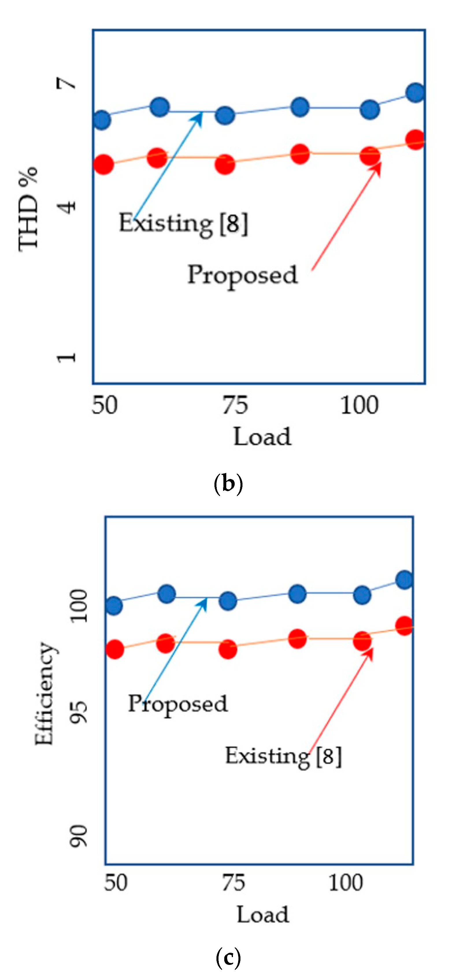
The pulse width modulation (PWM) of the switches is controlled using an output light-emitting diode (LED) light. The control flowchart is shown in Figure 4.
Dimming mode linearity and futures-based PWM have been extensively used for operating high-luminosity LED outputs. The light level is changed by changing the duty cycle, i.e., the average output current of the DC–DC converter output is controlled by PWM. The current–luminance characteristics of an LED are nonlinear in nature. Conventional methods are not suitable for obtaining higher efficiencies. The algorithm mainly focuses on further improvement in the luminous efficiency by using dimming manipulation. The error is calculated from the LED output using a sensor as well as a heat sink and the junction temperature. By varying the PWM, an accurate output is obtained.

3. Results

A 2 kW prototype model was developed for practical experiments; the input DC voltage to the circuit was 400 V. A detailed converter specification is given in Table 1. A grid simulator with a rectifier was used for the supply voltage.
The control board design is from an Intel CPLD and includes a micro controller unit for the implementation of the control algorithm. The experimental setup is shown in Figure 5. The switches and other components used in the hardware prototype model are listed in Table 2. The voltage and current waveforms of the experiment are as shown in Figure 6a. The steady state performance of the converter operation is shown in Figure 6b.
Switches Q1 and Q3 have a similar pattern of soft switching. Under ZCS, switch Q3 is turned ON during mode 1, and its output is as shown in Figure 6b. The hardware output waveforms of ZVS and ZCS at ZVS limited peak voltage condition are shown in Figure 7a. Furthermore, the switch current waveform when ZCS is OFF and the switch current waveform when ZCS is ON are shown in Figure 7b and Figure 7c, respectively. The increasing slope of the collector current is controlled by the LL inductor. Because switch Q1 is ON, the current gradually decreases, as discussed for mode 2, provided ZCS from switch Q3 is turned OFF. The LL inductor current slowly reduces and flows via D1 and D3, so the reverse recovery losses of the diodes are low. The current flowing from diode D1 to switch Q3 is lower due to a small reverse recovery time during the second mode, as is shown in Figure 8a. Switches Q2 and Q4 have soft switching characteristics which take effect under ZVS and ZCS conditions, as is shown in Figure 7b and Figure 7c, respectively.
ZCS is turned ON by applying a control pulse to the gate during freewheeling operation in the fourth mode. ZCS is turned OFF with the help of the clamp capacitor, which is shown in Figure 8d. The transient response is shown using the control algorithm for a converter operation load between 1.5 kW and 2 kW. The results show that disturbances in the bus DC voltage are decreased during the transition of the load, which is compensated by the connected RC. An input voltage of up to 400 V is applied to the circuit using a grid simulator. The input voltage and DC bus voltage are restored during stable operation.
The system performance was studied under different load values up to 2 kW. A passive clamp capacitor was connected with a high frequency transformer. This type of converter has a relatively higher total demand distortion since the clamp capacitor circulates stored energy inside the circuit. Thus, distortion occurs in the current and is highly prominent near zero crossing. The LACF circuit energy is released again and freewheels. The stored capacitor power is omitted in the converter circuit. The total demand distortion of the proposed topology is less than 3.2% under all load conditions. The experimental results are provided in Table 3 and the power loss distribution is displayed in Figure 9.
The power loss is calculated during full load, with the bridge of the input source consuming 3% (1.92 W). The output side components consume 20.20% (12.968 W) and the output side switch loss is 20.20% (12.968 W). The input side components consume 18.7% (11.968 W) and the input and side switches consume 12.1% (7.744 W). Finally, the magnetic circuit loss is 19.60% (12.544 W). The total losses from the circuit components during full load are 3.2%. The total power losses, calculated via a thermal analysis, amount to 64 W, so the output power is 1.936 kW for an input power of 2 kW. Therefore, the maximum efficiency of the circuit is 96.8%.
Topology comparisons were made between the proposed topology and existing topologies from the literature, and these are shown in Table 4. The topology in [5] has a lower switch count, and the DC link capacitors are not required, while the obtained efficiency is 92.3%. In [18], the topology is designed with 12 IGBTs and a control circuit, but the overall efficiency is 93.6%, and additional components are used, which increases the circuit cost. These switching devices increase electromagnetic interference, so electromagnetic interference filters are required. The proposed converter was further compared with other existing converters [21,25]. The converters in [25] needed additional filters to obtain soft switching, and tuning was required with different loading. The proposed converter uses only six IGBTs and an isolated gate driver circuit.
A cost analysis and converter development analysis were also made for the input side. The maximum voltage applied in the input side was 400 V DC and the diodes in the input side were inactive in the OFF state. Schottky diodes were used for ultrafast reverse recovery in the input and output sides to improve efficiency. The range of the power factor was 0.988–0.999, and the value is shown in Figure 10. The THD value of the input side, determined using a fast Fourier series analysis, was 3.45%, as is shown in Figure 11a. The converter also yielded a lower total demand distortion in the range of 3.1% to 3.5%, as is shown in Figure 11b. Two flyback converters with a power of 20 W were used in the clamp circuit in this prototype model. Thus, a leakage inductor with a value of 170 µ Henry was selected. The maximum efficiency during a full load was 96.8%, as is shown in Figure 11c. These two converters were combined for further improvements.

4. Conclusions

An isolated DC–DC LACF-based converter that provides voltage regulation in a conversion stage is proposed. The proposed LACF-based converter has a clamp circuit that can recycle energy twice per cycle. The proposed circuit works under a continuous conduction mode and is controlled by a luminous control algorithm. The experimental prototype model was validated with a maximum power of 2 kW. The experimental output demonstrated soft switching during all load conditions. The dynamic performance of the converter was also evaluated during load-changing conditions. The converter also yielded a lower total demand distortion (in a range of 3.1% to 3.5%). The maximum efficiency during full load was calculated to be 96.8%, which is higher than that of any existing topology.

Author Contributions

Conceptualization, A.S.V. and K.S.; Methodology, K.S.; Software, A.S.V. and K.S.; Validation, A.S.V. and K.S.; Formal analysis, K.R.R. and J.V.; Investigation, K.S. and P.S.R.; Data curation, K.S.; Writing—original draft, A.S.V.; Writing—review & editing, P.S.R., K.R.R., J.V. and A.A.S.; Supervision, A.A.S. All authors have read and agreed to the published version of the manuscript.

Funding

This research received no external funding.

Data Availability Statement

The data that support the findings of this study are available from the corresponding author upon request.

Conflicts of Interest

The authors declare no conflict of interest.

References

  1. Satya Veerendra, A.; Rusllim Mohamed, M.; Punya Sekhar, C. Modelling and analysis of voltage balancing topology for series-connected supercapacitor energy storage system. Int. J. Model. Simul. 2023, 1–14. [Google Scholar] [CrossRef]
  2. Tran, T.N.T.; Wang, H.-C.; Wang, J.-M. A Dual-Mode Control Scheme to Improve Light Load Efficiency for Active-Clamp Flyback Converter. Electronics 2022, 11, 1308. [Google Scholar] [CrossRef]
  3. Naresh, S.V.K.; Peddapati, S.; Alghaythi, M.L. A Novel High Quadratic Gain Boost Converter for Fuel Cell Electric Vehicle Applications. IEEE J. Emerg. Sel. Top. Ind. Electron. 2023, 4, 637–647. [Google Scholar] [CrossRef]
  4. Rajabi, A.; Shahir, F.M.; Sedaghati, R. Output voltage improvement of fuel cell electric vehicles based on a novel high step-up DC–DC converter. AEU-Int. J. Electron. Commun. 2023, 162, 154574. [Google Scholar] [CrossRef]
  5. Ortega, Á.; Milano, F. Efficiency and conducted EMI evaluation of a single-phase power factor correction boost converter using state-of-the-art SiC mosfet and SiC diode. IEEE Trans. Power Syst. 2016, 31, 3369–3380. [Google Scholar] [CrossRef]
  6. Veerendra, A.S.; Mohamed, M.R.; Sulaiman, M.H.; Sudhakar, K.; Peddakapu, K. Modelling and simulation of dual sourced front-end converter for hybrid electric vehicles. Int. J. Ambient Energy 2020, 43, 1646–1653. [Google Scholar] [CrossRef]
  7. Byrne, R.H.; Nguyen, T.A.; Copp, D.A.; Chalamala, B.R.; Gyuk, I. Energy Management and Optimization Methods for Grid Energy Storage Systems. IEEE Access 2018, 6, 13231–13260. [Google Scholar] [CrossRef]
  8. Zhang, Z.; Zhang, Y.; Huang, Q.; Lee, W. Market-oriented optimal dispatching strategy for a wind farm with a multiple stage hybrid energy storage system. CSEE J. Power Energy Syst. 2018, 4, 417–424. [Google Scholar] [CrossRef]
  9. Nishikawa, N.; Nakano, M.; Kitsuregawa, M. Application Sensitive Energy Management Framework for Storage Systems. IEEE Trans. Knowl. Data Eng. 2015, 27, 2335–2348. [Google Scholar] [CrossRef]
  10. Lee, J.; Lee, K. Carrier-Based Discontinuous PWM Method for Vienna Rectifiers. IEEE Trans. Power Electron. 2015, 30, 2896–2900. [Google Scholar] [CrossRef]
  11. Dash, D.K.; Sadhu, P.K. A Review on the Use of Active Power Filter for Grid-Connected Renewable Energy Conversion Systems. Processes 2023, 11, 1467. [Google Scholar] [CrossRef]
  12. Smadi, A.A.; Khoucha, F.; Amirat, Y.; Benrabah, A.; Benbouzid, M. Active Disturbance Rejection Control of an Interleaved High Gain DC–DC Boost Converter for Fuel Cell Applications. Energies 2023, 16, 1019. [Google Scholar] [CrossRef]
  13. Hao, X.; Salhi, I.; Laghrouche, S.; Ait-Amirat, Y.; Djerdir, A. Nonlinear Disturbance Observer-based sliding mode control of interleaved boost converter for fuel cell used in microgrids. IFAC-PapersOnLine 2022, 55, 665–670. [Google Scholar] [CrossRef]
  14. Al-Hitmi, M.A.; Moinoddin, S.; Iqbal, A.; Rahman, K.; Meraj, M. Space vector vs. sinusoidal carrier-based pulse width modulation for a seven-phase voltage source inverter. CPSS Trans. Power Electron. Appl. 2019, 4, 230–243. [Google Scholar] [CrossRef]
  15. Huang, Q.; Huang, A.Q. Feedforward Proportional Carrier-Based PWM for Cascaded H-Bridge PV Inverter. IEEE J. Emerg. Sel. Top. Power Electron. 2018, 6, 2192–2205. [Google Scholar] [CrossRef]
  16. Lee, J.; Lee, K. Performance Analysis of Carrier-Based Discontinuous PWM Method for Vienna Rectifiers with Neutral-Point Voltage Balance. IEEE Trans. Power Electron. 2016, 31, 4075–4084. [Google Scholar] [CrossRef]
  17. Ye, M.; Chen, L.; Kang, L.; Li, S.; Zhang, J.; Wu, H. Family of enhanced ZCS single-stage single-phase isolated AC–DC converter for high-power high-voltage DC supply. IEEE Access 2019, 7, 53152–53162. [Google Scholar] [CrossRef]
  18. Jiang, W.; Huang, X.; Wang, J.; Wang, J.; Li, J. A Carrier-Based PWM Strategy Providing Neutral-Point Voltage Oscillation Elimination for Multi-Phase Neutral Point Clamped 3-Level Inverter. IEEE Access 2019, 7, 124066–124076. [Google Scholar] [CrossRef]
  19. Tseng, S.-Y.; Fan, J.-H. Zeta/Flyback Hybrid Converter for Solar Power Applications. Sustainability 2022, 14, 2924. [Google Scholar] [CrossRef]
  20. Wang, B.; Dehghanian, P.; Wang, S.; Mitolo, M. A high-frequency-link single-phase PWM rectifier. IEEE Trans. Ind. Electron. 2019, 55, 6603–6612. [Google Scholar]
  21. Venkatesan, M.; Adhavan, B.; Suresh, K.; Balachander, K. Lordwin Cencil Prabakar, Research on FPGA controlled three phase PV inverter using multi-carrier PWM control schemes. Microprocess. Microsyst. 2020, 76, 103089. [Google Scholar] [CrossRef]
  22. Eghtedarpour, N.; Farjah, E. Distributed charge/discharge control of energy storages in a renewable-energy-based DC micro-grid. IET Renew. Power Gener. 2014, 8, 45–57. [Google Scholar] [CrossRef]
  23. Pandi, P.; Subbarao, M.; Suresh, K. HBC-Based 3Ø System for Wide Range of Power Conversion. IEEE Can. J. Electr. Comput. Eng. 2021, 44, 321–328. [Google Scholar] [CrossRef]
  24. Saravanan, R.; Suresh, K. Integrated DC-AC and AC-DC Converter Using H-Converter for wide range voltage applications. Circuit World 2021, 48, 139–146. [Google Scholar]
  25. Li, C.; Zhang, Y.; Cao, Z.; Xu, D. Single-phase single-stage isolated ZCS current-fed full-bridge converter for high-power AC/DC applications. IEEE Trans. Power Electron. 2017, 32, 6800–6812. [Google Scholar] [CrossRef]
  26. Büyük, M.; Savrun, M.M.; İnci, M. Analysis and modeling of wireless power transfer supported by quadratic boost converter interfaced fuel cell power source. Int. J. Numer. Model. Electron. Netw. Devices Fields 2022, 35, e2997. [Google Scholar] [CrossRef]
  27. Veerendra, A.S.; Shah, A.A.; Mohamed, M.R.; Sekhar, C.P.; Leung, P. Wavelet Transform Based Fault Identification and Reconfiguration for a Reduced Switch Multilevel Inverter Fed Induction Motor Drive. Electronics 2021, 10, 1023. [Google Scholar] [CrossRef]
  28. Srinivasan, S.; Tiwari, R.; Krishnamoorthy, M.; Lalitha, M.P.; Raj, K.K. Neural network based MPPT control with reconfigured quadratic boost converter for fuel cell application. Int. J. Hydrogen Energy 2021, 46, 6709–6719. [Google Scholar] [CrossRef]
  29. Henao-Bravo, E.E.; Ramos-Paja, C.A.; Saavedra-Montes, A.J. Adaptive control of photovoltaic systems based on dual active bridge converters. Computation 2022, 10, 89. [Google Scholar] [CrossRef]
  30. Meng, X.; Jia, Y.; Xu, Q.; Ren, C.; Han, X.; Wang, P. A novel intelligent nonlinear controller for dual active bridge converter with constant power loads. IEEE Trans. Ind. Electron. 2022, 70, 2887–2896. [Google Scholar] [CrossRef]
  31. Akhtar, M.F.; Raihan, S.R.S.; Rahim, N.A.; Akhtar, M.N.; Bakar, E.A. Recent developments in DC–DC converter topologies for light electric vehicle charging: A critical review. Appl. Sci. 2023, 13, 1676. [Google Scholar] [CrossRef]
  32. Tarzamni, H.; Gohari, H.S.; Sabahi, M.; Kyyrä, J. Non-isolated high step-up dc-dc converters: Comparative review and metrics applicability. IEEE Trans. Power Electron. 2023, 1–41. [Google Scholar] [CrossRef]
  33. Kokkonda, R.K.; Beddingfield, R.; Bhattacharya, S.; Carsten, B.; Varga, B. A Novel Transformer Leakage Energy Recovery Active Clamp Control Technique for High Power AC/DC Flyback Converters. In Proceedings of the 2023 IEEE Applied Power Electronics Conference and Exposition (APEC), Orlando, FL, USA, 19–23 March 2023; pp. 1238–1245. [Google Scholar]
  34. Zhang, Z.; He, X.-F.; Liu, Y.-F. An optimal control method for photovoltaic grid-tied-interleaved flyback microinverters to achieve high efficiency in wide load range. IEEE Trans. Power Electron. 2013, 28, 5074–5087. [Google Scholar] [CrossRef]
  35. Hu, H.; Harb, S.; Kutkut, N.H.; Shen, Z.J.; Batarseh, I. A single-stage microinverter without using eletrolytic capacitors. IEEE Trans. Power Electron. 2012, 28, 2677–2687. [Google Scholar] [CrossRef]
  36. Kim, J.-G.; Kim, K.-D.; Noh, Y.-S.; Jung, Y.-C.; Won, C.-Y. Analysis and design of a three-port flyback inverter using an active power decoupling method to minimize input capacitance. J. Power Electron. 2013, 13, 558–568. [Google Scholar] [CrossRef]
  37. Sathiya, R.; Arun Noyal Doss, M. Design and implementation of single switch integrated boost and flyback converter for renewable and sustainable energy. PLoS ONE 2023, 18, e0287770. [Google Scholar] [CrossRef]
  38. Wang, C.; Sun, D.; Zhang, X.; Hu, J.; Gu, W.; Gui, S. A constant current digital control method for primary-side regulation active-clamp flyback converter. IEEE Trans. Power Electron. 2020, 36, 7307–7318. [Google Scholar] [CrossRef]
  39. Arshak, K.I.; Almukhtar, B. The design and development of a novel flyback planar transformer for high frequency switch mode DC–DC converter applications. Microelectron. J. 2000, 31, 929–935. [Google Scholar] [CrossRef]
  40. Goudarzian, A.; Khosravi, A.; Raeisi, H.A. Modeling, design and control of a modified flyback converter with ability of right-half-plane zero alleviation in continuous conduction mode. Eng. Sci. Technol. Int. J. 2022, 26, 101007. [Google Scholar] [CrossRef]
Figure 1. Proposed converter.
Processes 11 02980 g001
Figure 2. (a) First mode (t1 to t2). (b) Second mode (t2 to t3). (c) Third mode (t3 to t4). (d) Fourth mode (t4 to t5). (e) Fifth mode (t5 to t6).
Processes 11 02980 g002aProcesses 11 02980 g002b
Figure 3. (a) Switching waveform. (b) Luminous MPPT flowchart.
Processes 11 02980 g003aProcesses 11 02980 g003b
Figure 4. Luminous flux-based control flow chart.
Processes 11 02980 g004
Figure 5. Hardware prototype model.
Processes 11 02980 g005
Figure 6. Hardware output waveforms. (a) Input voltage and current. (b) Steady state output.
Processes 11 02980 g006aProcesses 11 02980 g006b
Figure 7. Hardware output waveforms of ZVS and ZCS. (a) Switch voltage waveform at ZVS limited peak voltage condition. (b) Switch current waveform when ZCS is OFF. (c) Switch current waveform when ZCS is ON.
Processes 11 02980 g007
Figure 8. Waveforms from dynamic load conditions. (a) Dynamic response during load changes. (b) Gate voltage (VGE). (c) Load response during load changes. (d) Clamping circuit output.
Processes 11 02980 g008aProcesses 11 02980 g008b
Figure 9. Power loss distribution.
Processes 11 02980 g009
Figure 10. Power from input AC–DC.
Processes 11 02980 g010
Figure 11. Results of analyses. (a) Fast Fourier series analysis. (b) THD comparison. (c) Efficiency comparison.
Processes 11 02980 g011aProcesses 11 02980 g011b
Table 1. Main device details.
DevicesNotationModel Number
Input switchesQ1–Q4MT5F515
DiodesDa, Db & D1–D8FD18S20
Control drive IC ACP-33J
Current sensor LA-55P
Voltage sensor LV25P
Simulator Chroma 6161
Table 2. Component details.
DevicesModel Number
Clamping capacitor3.3 nf
Clamping inductor150 micro farad
Inductor (input side)1 mH
Leakage inductor10 micro henry
Output capacitor2 × 550 micro farad
Transformer coreEE-85B
Table 3. Experiment results.
ParameterOutput Value
Pi (Power input)2 kW
VO (Voltage output)400 V
Vi (Voltage output)250 V
Frequency60 Hz
Switching frequency50 KHz
Turns ratio40:60
Table 4. Circuit comparisons.
ComponentZhang et al. [8]Li et al. [25]Proposed
DiodeFourFourTwo
CapacitorTwoTwoTwo
IGBTTwoTwoTwo
TransformerMainMainAux.
Rating (Vo)VdcVdcVdc
Rating (Vi)ViViVi
RecyclingPartialPartialFull
Recovery loss (diode)HighLowLow
Switching lossHighLowLow
Disclaimer/Publisher’s Note: The statements, opinions and data contained in all publications are solely those of the individual author(s) and contributor(s) and not of MDPI and/or the editor(s). MDPI and/or the editor(s) disclaim responsibility for any injury to people or property resulting from any ideas, methods, instructions or products referred to in the content.

