Article

Effects of Coating Parameters of Hot Filament Chemical Vapour Deposition on Tool Wear in Micro-Drilling of High-Frequency Printed Circuit Board

1
State Key Laboratory in Ultra-Precision Machining Technology, Department of Industrial and Systems Engineering, The Hong Kong Polytechnic University, Kowloon, Hong Kong, China
2
State Key Laboratory of Precision Electronic Manufacturing Technology and Equipment, Guangdong University of Technology, Guangzhou 510006, China
3
Techmart (Shenzhen) Limited, 2F, Block 2, No. 2 Chongqing Road, Qiaotou Community, Fuyong Subdistrict, Bao’an District, Shenzhen 518104, China
*
Authors to whom correspondence should be addressed.
Processes 2022, 10(8), 1466; https://doi.org/10.3390/pr10081466
Submission received: 28 June 2022 / Revised: 23 July 2022 / Accepted: 25 July 2022 / Published: 27 July 2022

Abstract

:
High-frequency and high-speed printed circuit boards (PCBs) are made of ceramic particles and anisotropic fibres, which are difficult to machine. In most cases, severe tool wear occurs when drilling high-frequency PCBs. To protect the substrate of the drills, diamond films are typically fabricated on the drills using hot filament chemical vapour deposition (HFCVD). This study investigates the coating characteristics of drills with respect to different HFCVD processing parameters and the coating characteristics following wear from machining high-frequency PCBs. The results show that the methane concentration, processing time and temperature all have a significant effect on the grain size and coating thickness of the diamond film. The grain size of the film obviously decreases as does the methane concentration, while the coating thickness increases. By drilling high-frequency PCBs with drills with nanocrystalline and microcrystalline grain sizes, it is discovered that drills with nanocrystalline films have a longer tool life than drills with microcrystalline films. The maximum length of the flank wear of the nanocrystalline diamond-coated drill is nearly 90% less than microcrystalline diamond-coated tools. Moreover, drills with thinner films wear at a faster rate than drills with thicker films. The findings highlight the effects of HFCVD parameters for coated drills that process high-frequency PCBs, thereby contributing to the production of high quality PCBs for industry and academia.

1. Introduction

As the world is accelerating into the 5G era, there are higher requirements for PCB transmission speeds and thermal design considerations. The new PCB design incorporates ceramic particles, which help increase the heat dissipation rate [1], but, in turn, lower the machinability of the workpiece. Researchers have extensively studied the relationship between drill coating thickness and grain when machining the PCBs of the third and fourth generations, such as the copper-clad resin-based FR-4 [2,3,4,5]. However, the relationships between the drill tool wear rate, the diamond coating thickness and grain size when machining PCBs of the fifth generation have still not been fully explored. Currently, high-frequency and high-speed PCBs have a wide range of needs and applications in 5G mobile communication technology due to their superior heat resistance and lower transmission loss when compared with conventional PCBs [6]. High-frequency and high-speed PCBs are made from a composite material that is composed of copper-clad laminate, ceramic particles, anisotropic fibres and epoxy resin [7,8]. In the manufacturing of high-frequency PCBs, micro drills are commonly used to fabricate micro holes on layers of printed circuit boards because of their high efficiency and the low cost. However, due to the high anisotropy and low thermal conductivity of general PCB drills, the rate of tool wear and hole quality are exceptionally high. PCB drills have to be capable of withstanding abrasive wear from ceramic fillers and adhesive wear from molten resin [8] adhering to the drills under high-temperature processing conditions. Friction and heat are generated during the drilling process. An increase in drilling temperature inside the hole causes the resin to melt, adhering to the wall of the hole and the drill tip and affecting the subsequent rotation of the drill bit. These two types of deterioration are primarily responsible for the tool becoming worn and broken before the end of its expected tool life.
To protect the substrate of the drills, the HFCVD technique is generally employed to fabricate diamond films on the drills. The novelty of the coating drill research is to determine the suitable coating thickness and grain size for high-speed board machining. It has been demonstrated that 4000 holes can be fabricated by HFCVD-coated drills without obvious drill wear, which is more than three times the lifespan of conventional non-coated drills [9]. Notably, different pretreatment methods and deposition parameters result in variations in the coating layer thickness and grain size of the diamond film, which can range from micrometres to nanometres. The main methods to fabricate microcrystalline diamond (MCD) and nanocrystalline diamond (NCD) film layers require gas mixtures and additional sources of energy such as thermal energy or plasma for the gas mixtures to dissociate and deposit on the substrate. While both coating types are applied to protect PCB drills, each has its own differential advantage. As MCD films and NCD films have different topographies and frictional coefficients, their cutting performance is different [10]. It is therefore important to identify the most critical processing condition in order to fabricate the optimum coating thickness and grain size of a drill for machining high-speed boards. Dawedeit et al. [11] found that the Young’s modulus is 950 GPa for the MCD layer and 730 GPa for the NCD layer, and that their grain sizes are inversely proportional to the workpiece roughness measured by atomic force microscopy (AFM). Chen et al. [12] discovered that the friction coefficient is 0.126 for the MCD and 0.076 for the NCD. Williams [13] stated that the friction coefficient of NCD-coated surfaces can be as low as those of single crystal diamonds. The MCD film can, relatively, adhere better to the substrate surface with higher wear resistance, resulting in better tool life. The NCD film has a relatively lower surface roughness, resulting in work with more refined surface finishes. The processing of a high-speed board necessitates a drill with high wear resistance for machining PCB components with ceramic fillers and a low surface roughness to reduce the possibility of the tool adhering to the molten resin.
In addition to affecting the mechanical properties of the thin films, the thickness of the coating layer influences the sharpness of the cutting edge, thus negatively impacting the drilling performance. Rare scientific journals have investigated the effects of coating thickness and grain size on the processing of high-frequency and high-speed PCBs. The purpose of this study was to investigate the quality of diamond films with varying MCD and NCD grain sizes and coating thicknesses in order to determine the effects of grain size and coating thickness on tool wear rates when drilling high-frequency PCBs, thereby enhancing the drilling performance of high-frequency PCBs.

2. Theory—Fabrication of Drills with MCD and NCD by HFCVD

Prior to the diamond film deposition, the surface of the PCB drills should be treated with Murakami’s solution (KOH:K3(Fe(CN)6:H2O = 1:1:10) and Caro’s acid (H2O2 + H2SO4) [14]. The Murakami treatment enables the WC to dissolve into the chemical solution and increase the surface roughness of the substrate surface. Caro acid is used to remove cobalt from the surface, preventing graphitisation during the diamond film growth process.
In the HFCVD diamond coating process, chemical gases are utilized as a carbon source and filaments are utilized to generate heat. The heat induces chemical reactions that generate diamond films on the surfaces of substrates. The HFCVD diamond coating process requires a hot filament to react with the carbon source input gas methane (CH4). The most common filament materials for HFCVD are tungsten (W) and tantalum (Ta). As given in Figure 1a, the carbon source CH4 and hydrogen (H2) pass through the hot filament at the start of the deposition process. When the hot pure tantalum filament begins to react with the mixed gas (methane and hydrogen), it causes filament carbonisation and embrittlement. After passing through the hot filament, the mixed gas receives enough thermal energy to break hydrogen bonds (H2, CH4) into atomic hydrogen (H0), as illustrated in Equation (1). This dissociation into atomic forms enables diamond growth. Hydrogen atoms (H0) can interact further with small hydrocarbon molecules (mostly CH4) to form methyl radicals (CH3) and diamond growth, according to Equation (2). As illustrated schematically in Figure 1a,b, the following chemical equations [15] apply:
H 2     H 0 + H 0
CH 4 + H 0     CH 3 + H 2
In this study, the diamond film on PCB drills is grown using the hot filament chemical vapour deposition (HFCVD) method. Several processing parameters, including temperature, methane concentrations and deposition durations, can be adjusted to stabilize the growth of the film. Different grain sizes and different coating thicknesses can be formed on the drills.

3. Experimental Procedures and Setup

In this study, PCB drills (∅1.1, 6% Co) tungsten carbide (WC) with grain size of 0.5–0.8 μm were selected. Drills of microcrystalline diamond (MCD) film and nanocrystalline diamond (NCD) film with coating thickness of 3 μm, 6 μm, 9 μm were investigated in this study, as shown in Table 1. The following parameters were specified for deposition: tool temperature between 800–900 °C; methane 20–80 sccm and deposition duration between 10–24 h. The temperature, deposition durations and CH4 concentration parameters were varied to investigate different grain growth rate and size of diamond films.
After diamond films had been deposited on the drills, scanning electron microscope (SEM) was used to observe the coating thickness and grain size of the coating films. The drills were then tested on Rogers 4350B high-frequency PCB using VEGA-D2CMSL drilling machine with feed rate of 2.4 m/min and spindle speed of 45,000 r/min. Boards were stacked together that consisted of 5 boards, 3 of which were phenolic boards with a thickness of 0.5 mm, and 2 of which were high-frequency PCB with a thickness of 0.8 mm, as shown in Figure 2. The condition of the drill (wearing) was observed when every 1000 holes were drilled. The micro drills were ultrasonically washed by acetone to remove the dirt after drilling. Then, wear was observed by digital microscope of KEYENCE VHX-7000 (e.g., flank wear at the major cutting edges). Surface morphology of the films was measured by atomic force microscopy (AFM) with size 10 μm × 10 μm sample regions; three different regions were measured in order to obtain the average value. The adhesion characteristics of films with different coating layer thickness and grain size were analysed by Rockwell indentation with a test force of 588 N.

4. Results and Discussion

4.1. Effects of Coating Parameters on Grain Size and Coating Thickness

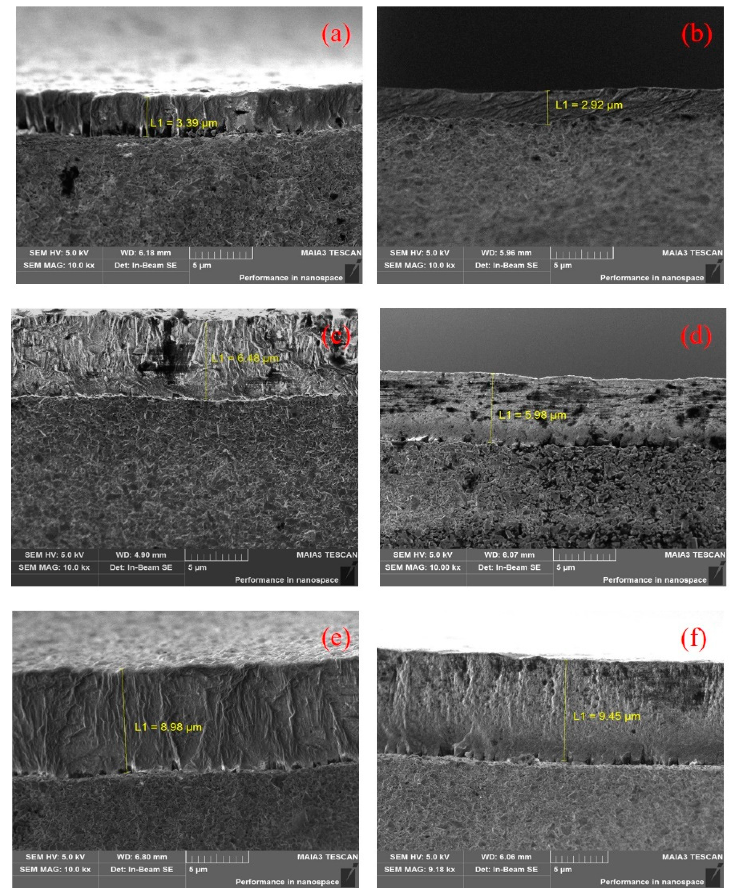
To investigate the control of the HFCVD-coated MCD and NCD films’ layer thicknesses and grain sizes, the influences of temperature, methane concentration and deposition time on the coating thickness and grain size were studied. The micro-topographies and cross-sectional profiles of the MCD and NCD films with 3 μm, 6 μm and 9 μm coating thicknesses are shown in Figure 3 and Figure 4. M1–M3 drills with MCD films exhibit sharp columnar crystal growth with clear grains of size between 2–4 μm while N1–N3 drills with NCD films exhibit cluster growth of nanosized diamond grains with a cauliflower-like morphology. The grain size and growth rates are different in accordance with the variety in methane, deposition duration and temperature, and the relationships are shown in Figure 4.
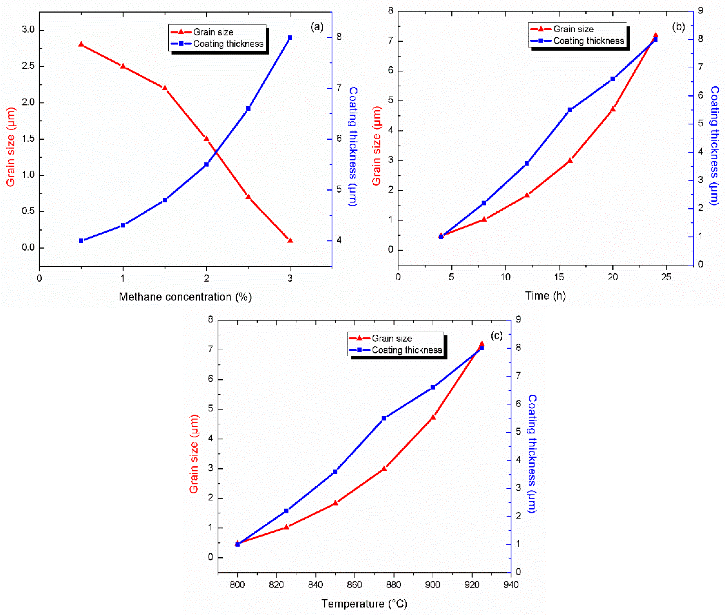
As shown in Figure 5a, an increase in methane concentration leads to a decrease in the grain size and an increase in coating thickness. The increased methane concentration enhances secondary nucleation [16,17] as there is not enough hydrogen to etch the non-diamond phase of the drill and to increase the rate of ion bombardment. In this case, the newly formed diamond film layer has a smaller grain size than its previous layer. More methane leads to more methyl radicals incorporated in the coating region, resulting in increases in the growth rate of the diamond film [18]. As represented in Figure 5b, as the duration of diamond film deposition in the HFCVD machine chamber increases, the average grain size and number of grains decrease [19]. In accordance with the experimental findings, the coating thickness increases from 1 μm to 9 μm as the duration increases from 4 to 24 h. As shown in Figure 5c, increasing the substrate temperature could increase the dissociation speed of H2, which results in a higher growth rate of the film/grain [20,21].

4.2. Effect of Coating Thickness and Grain Size on Adhesion Strength

Rockwell A with the load of 588 N was selected to evaluate the diamond coating adhesion on WC-Co substrates. Figure 6 shows SEM images of the Rockwell indentations on the tool surfaces with 3 μm, 6 μm and 9 μm MCD and NCD diamond coating layers. Two major defective results were observed: crack propagation and coating delamination. The diameters of the cracks upon delamination measured on six samples, M1–M3 and N1–N3, were 120 μm, 110 μm, 101 μm, 158 μm, 135 μm and 130 μm, respectively. The deformation area can be ranked as: M3, M2, M1, N3, N2 and N1. Cracks were observed on both the MCD and NCD films with 3 μm and 6 μm thicknesses. No crack propagation was initiated on the surfaces of samples with 9 μm MCD (M3) and NCD coating thickness (N3). Coating delamination occurred on MCD and NCD films with 3 μm and 6 μm thickness. The samples with 3 μm coating layers showed greater coating delamination than the 6 μm coating layers, implying that coating adhesion is stronger in thicker films. In summary, coating thickness was the critical factor influencing the adhesive strength of the diamond film, as neither M3 nor N3 observed crack propagation after indentation.

4.3. Effect of Coating Thickness and Grain Size on Surface Roughness

Just as depicted by the SEM images in Figure 4, the AFM images in Figure 7 show the same structures of the MCD and NCD films. AFM images of the diamond films with the size 10 μm × 10 μm are demonstrated in Figure 7. The means of the surface roughness of the M1–M3 and N1–N3 drills were 91.4 nm, 107.6 nm, 123.0 nm, 22.3 nm, 25.7 nm and 27.8 nm, respectively. MCD films appeared to have higher surface roughness due to the uneven grain sizes. NCD films appeared to have lower surface roughness due to smaller grains and lower coefficient of friction. According to the results, coating thickness is not the primary factor affecting surface roughness, with surface roughness increasing by 32 nm from M1 to M3 and 5 nm from N1 to N3. The results indicate that film grain size is the main influence on surface roughness, whereas coating thickness has a minimal impact among other factors shown in this study.

4.4. Investigation on Tool Wear

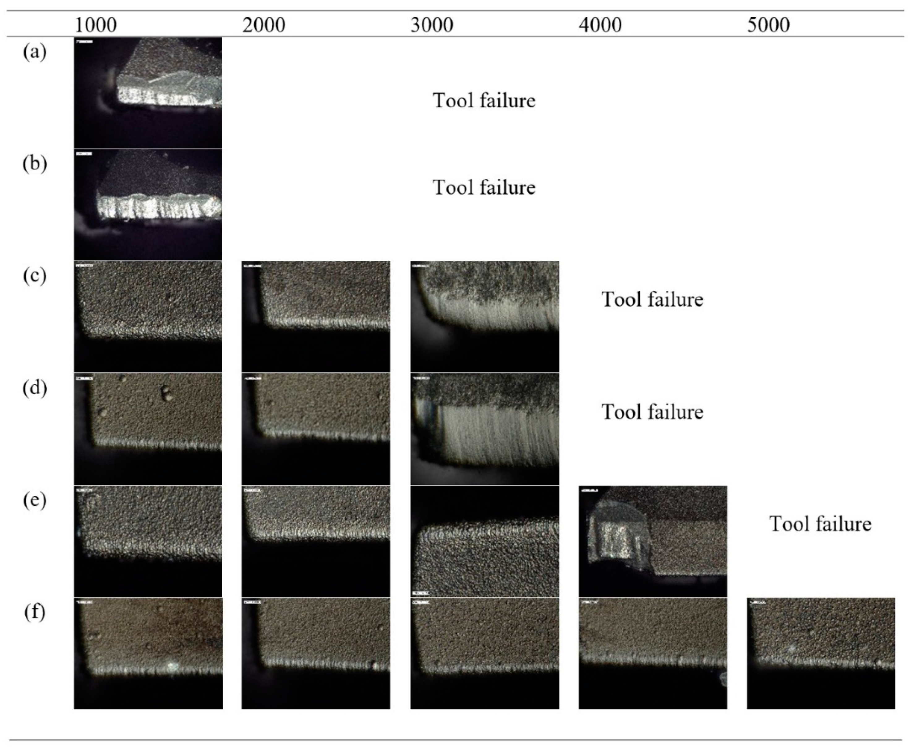
To study the tool wear states, six drills with different grain sizes and film thicknesses were used to manufacture micro holes on high-frequency PCBs. As shown in Figure 8, significant abrasive wear was observed on the flank face of both the MCD and the NCD drill with a 3 μm coating thickness after processing 1000 holes, causing coating delamination. The 3 μm NCD-coated drill (N1) exhibited more damage than the 3 μm MCD-coated drill (M1) as the substrate material of the cutting edge was also removed. This indicates that compared with MCD drills, NCD drills have a longer tool life due to the lower adhesion of the diamond film on the WC-Co substrate.
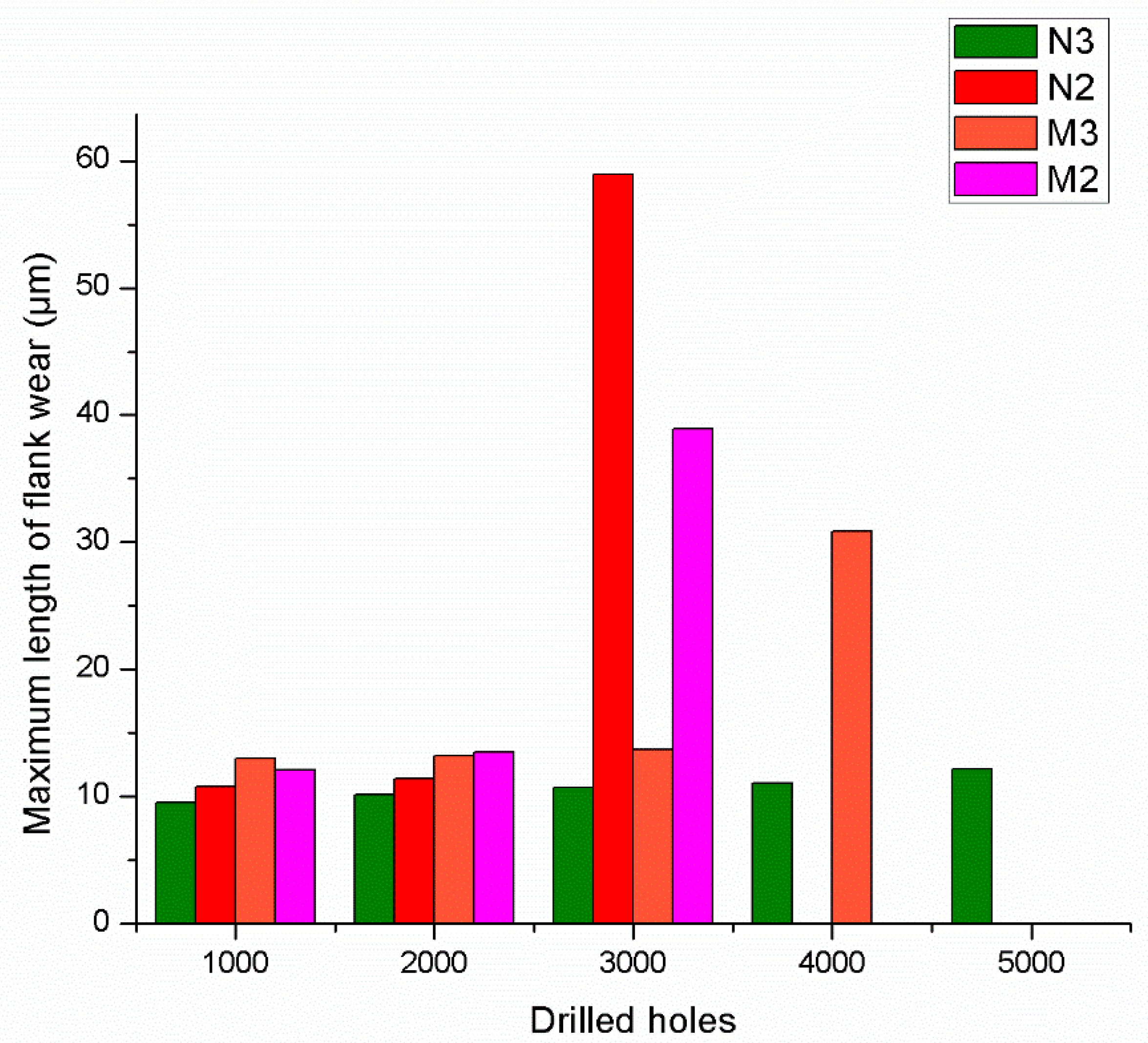
A comparison of the NCD drill wear between coating thicknesses of 6 μm and 9 μm (N2, N3) after drilling 3000 holes was conducted. Even though significant abrasive tool wear can be observed on the NCD drills with a 6 μm coating thickness (N2). The tool wear of N3 increased steadily during the experiment, with the maximum lengths of flank wear for N3 from 1000 to 5000 holes being 9.54 μm, 10.12 μm, 10.68 μm, 11.05 μm and 12.17 μm, respectively. No obvious tool wear or coating delamination occurred for 9 μm (N3) after drilling 5000 holes. It could be explained that the NCD film layer’s thickness is sufficient to resist both abrasive wear and adhesive wear from processing 5000 holes due to its adhesion characteristics and smooth surface.
In drilling high-frequency PCBs, drills need to withstand abrasive wear from the ceramic layer and adhesive wear from the molten resin adhering to the drill following friction and heat generated from the process [2]. Figure 9 shows the maximum length of the flank wear of MCD and NCD drills with different coating thicknesses. It is learned that NCD-coated drills can outperform MCD-coated drills. In addition, the thicker the coating layer, the less chance the drilling force is distributed onto the drill substrate layer [22]. Thereby, localised delamination is reduced, and elasticity and the resistance to abrasive wear are increased. The tool wear of M1 and N1 is not illustrated on Figure 9 given the fact that the maximum length of flank wear of M1 and N1 cannot be measured due to the delamination of the tool cutting edge after drilling 1000 holes. The tools’ lifespan can rank as: N3, M3, M2, N2, M1 and N1. The maximum length of the flank wear of the NCD drill is nearly 90% less than the MCD drill.

4.5. Investigation on PCB Hole Wall Roughness

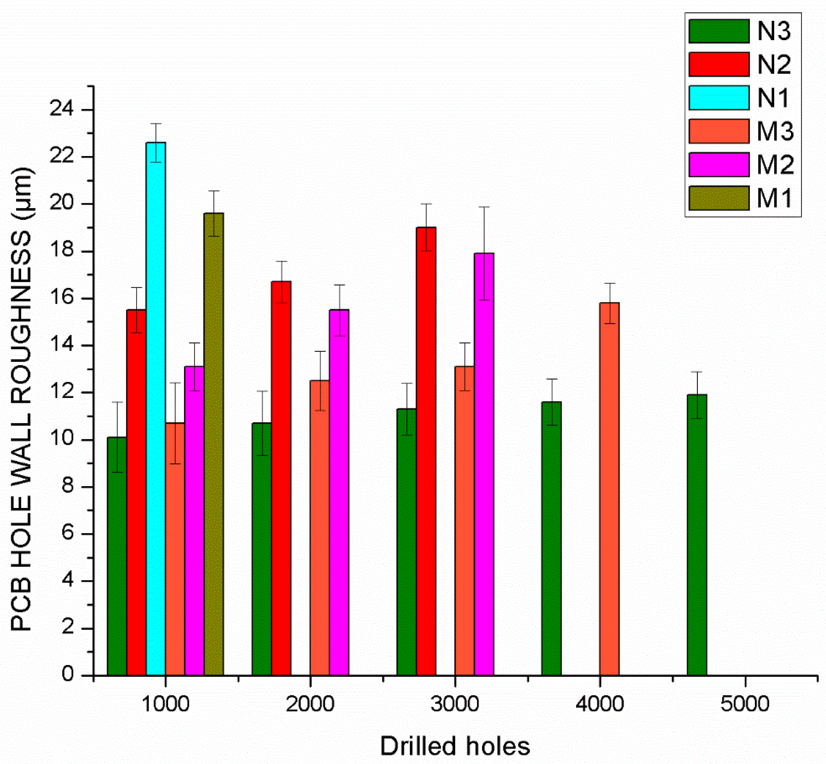
Figure 10 describes the wall roughness of the PCB hole walls after being manufactured, which is one of the main criteria for judging the quality of finished PCBs [7]. Dimensional accuracy, the presence of entry and exit burrs, the smear of resin on the sides of holes and delamination are also characteristics of the workpiece to be examined. Drill film grain size and thickness determine the quality of finished holes. As shown in Figure 10, the results show that the surface roughness of the PCB holes decreases as the coating thickness increases. When 3 μm-MCD-coated drills (M1) are compared to 3-μm-NCD-coated drills (N1), and 6-μm-MCD-coated drills (M2) are compared to 6-μm-NCD-coated drills (N2), the MCD-coated ones produce better hole quality than the NCD-coated ones. On the other hand, 9-μm-NCD-coated drills (N3) can drill more than 5000 holes with a smooth surface, whereas 9-μm-MCD-coated drills (M3) do not perform well after 3000 holes. The surface roughness of the PCB holes drilled by an NCD-coated drill is 30% better than MCD according to Figure 10. The quality of PCB holes is actually highly dependent on the drill condition. The roughness of the workpiece hole wall increases significantly as the tool deteriorates. Surface roughness of the drill coating layer has a direct impact on the surface roughness of the processed PCB hole wall. On the other hand, according to the AFM results shown in Figure 7, the surface roughness of the NCD film is much lower than the MCD film. Low surface roughness enhances the chip removal process: molten resin can be easily removed from the flute [4]. Therefore, the tool geometry is maintained and the possibilities of delamination and microcracks on the PCB workpiece are reduced.

5. Conclusions

The purpose of this study is to determine the effects of the grain size and coating thickness of the diamond film on the drilling performance of high-frequency and high-speed printed circuit boards (PCB), thereby contributing to the relevant industries and academia. The major conclusions that can be drawn from this study are as follows:
  • As methane concentration increases, the grain size of the diamond film changes from microcrystalline to nanocrystalline, which is inversely proportional to temperature and time.
  • A thicker coating can protect the substrate of the drills well as the drilling force applied is spread across the coating layer instead of the substrate of the tool according to the Rockwell indentation, with no crack propagation or coating delamination between the diamond film and substrates when the thickness is 9 μm.
  • The advantage of a thicker diamond coating layer is that the drill is more durable and resistant to wear. For drills with a thicker coating layer, the drilling force applied is distributed throughout the coating layer. For drills with a thinner coating layer, the drilling force is supported by the substrate itself and the coating layer. Localised delamination is reduced as the adhesion is proportional to the film thickness.

Author Contributions

Conceptualization, F.M.K. and Z.S.; methodology, F.M.K.; software, F.M.K. and Z.S.; validation, W.S.Y. and S.T.; formal analysis, F.M.K.; investigation, F.M.K.; resources, S.T.; data curation, F.M.K. and Z.S.; writing—original draft preparation, F.M.K. and Z.S.; writing—review and editing, W.S.Y.; visualization, F.M.K., Z.S. and W.S.Y.; supervision, W.S.Y. and S.T.; funding acquisition, K.Y.D.K. and S.T. All authors have read and agreed to the published version of the manuscript.

Funding

This research was funded by the National Natural Science Foundation of China (No. 52005110, 51975128) and Innovation and Technology Commission (ITS/246/18FX).

Institutional Review Board Statement

Not applicable.

Informed Consent Statement

Not applicable.

Data Availability Statement

Not applicable.

Acknowledgments

This work was supported partially by the National Natural Science Foundation of China and the Innovation and Technology Commission.

Conflicts of Interest

The authors declare no conflict of interest.

References

  1. Zhang, W.; Lu, C.; Ge, M.; Bu, F.; Zhang, J. Surface Modified and Gradation-Mixed Al2O3 as an Effective Filler for the Polyphenylene Oxide (PPO) Insulative Layer in Copper Clad Laminates. J. Mater. Sci. Mater. Electron. 2020, 31, 21602–21616. [Google Scholar] [CrossRef]
  2. Wang, Y.; Zou, B.; Yin, G. Wear Mechanisms of Ti(C7N3)-Based Cermet Micro-Drill and Machining Quality during Ultra-High Speed Micro-Drilling Multi-Layered PCB Consisting of Copper Foil and Glass Fiber Reinforced Plastics. Ceram. Int. 2019, 45, 24578–24593. [Google Scholar] [CrossRef]
  3. Zheng, L.; Wang, C.; Zhang, X.; Song, Y.; Zhang, L.; Wang, K. The Entry Drilling Process of Flexible Printed Circuit Board and Its Influence on Hole Quality. Circuit World 2015, 41, 147–153. [Google Scholar] [CrossRef]
  4. Lei, X.L.; He, Y.; Sun, F.H. Optimization of CVD diamond coating type on micro drills in PCB machining. Surf. Rev. Lett. 2016, 23, 1–8. [Google Scholar] [CrossRef]
  5. Zheng, L.; Wang, C.; Zhang, X.; Huang, X.; Song, Y.; Wang, K.; Zhang, L. The Tool-Wear Characteristics of Flexible Printed Circuit Board Micro-Drilling and Its Influence on Micro-Hole Quality. Circuit World 2016, 42, 162–169. [Google Scholar] [CrossRef]
  6. Huang, X.; Wang, C.; Yang, T.; He, Y.; Li, Y.; Zheng, L. Wear Characteristics of Micro-Drill during Ultra-High Speed Drilling Multilayer PCB Consisting of Copper Foil and Ceramic Particle Filled GFRPs. Procedia CIRP 2020, 101, 326–329. [Google Scholar] [CrossRef]
  7. Watanabe, H.; Tsuzaka, H.; Masuda, M. Microdrilling for Printed Circuit Boards (PCBs)-Influence of Radial Run-out of Microdrills on Hole Quality. Precis. Eng. 2008, 32, 329–335. [Google Scholar] [CrossRef]
  8. Zheng, L.J.; Wang, C.Y.; Fu, L.Y.; Yang, L.P.; Qu, Y.P.; Song, Y.X. Wear Mechanisms of Micro-Drills during Dry High Speed Drilling of PCB. J. Mater. Process. Technol. 2012, 212, 1989–1997. [Google Scholar] [CrossRef]
  9. Gäbler, J.; Schäfer, L.; Westermann, H. Chemical Vapour Deposition Diamond Coated Microtools for Grinding, Milling and Drilling. Diam. Relat. Mater. 2000, 9, 921–924. [Google Scholar] [CrossRef]
  10. Wang, H.; Wang, C.; Wang, X.; Sun, F. Effects of Carbon Concentration and Gas Pressure with Hydrogen-Rich Gas Chemistry on Synthesis and Characterizations of HFCVD Diamond Films on WC-Co Substrates. Surf. Coat. Technol. 2021, 409, 126839. [Google Scholar] [CrossRef]
  11. Dawedeit, C.; Kucheyev, S.O.; Shin, S.J.; Willey, T.M.; Bagge-Hansen, M.; Braun, T.; Wang, Y.M.; El-Dasher, B.S.; Teslich, N.E.; Biener, M.M.; et al. Grain Size Dependent Physical and Chemical Properties of Thick CVD Diamond Films for High Energy Density Physics Experiments. Diam. Relat. Mater. 2013, 40, 75–81. [Google Scholar] [CrossRef]
  12. Chen, N.; Shen, B.; Yang, G.; Sun, F. Tribological and Cutting Behavior of Silicon Nitride Tools Coated with Monolayer- and Multilayer-Microcrystalline HFCVD Diamond Films. Appl. Surf. Sci. 2013, 265, 850–859. [Google Scholar] [CrossRef]
  13. Williams, O.A. Nanocrystalline Diamond. Diam. Relat. Mater. 2011, 20, 621–640. [Google Scholar] [CrossRef]
  14. Peters, M.G.; Cummings, R.H.; National Center for Manu-facturing Sciences. Methods for Coating Adherent Diamond Films on Cemented Tungsten Carbide Substrates. U.S. Patent 5,236,740, 17 August 1993. [Google Scholar]
  15. Asmussen, J.; Reinhard, D.K. (Eds.) Diamond Films Handbook; CRC Press: Boca Raton, FL, USA, 2002; ISBN 0824795776. [Google Scholar]
  16. Wei, Q.; Yu, Z.M.; Ashfold, M.N.R.; Chen, Z.; Wang, L.; Ma, L. Effects of Thickness and Cycle Parameters on Fretting Wear Behavior of CVD Diamond Coatings on Steel Substrates. Surf. Coat. Technol. 2010, 205, 158–167. [Google Scholar] [CrossRef]
  17. Wiora, M.; Brühne, K.; Flöter, A.; Gluche, P.; Willey, T.M.; Kucheyev, S.O.; Van Buuren, A.W.; Hamza, A.V.; Biener, J.; Fecht, H.J. Grain Size Dependent Mechanical Properties of Nanocrystalline Diamond Films Grown by Hot-Filament CVD. Diam. Relat. Mater. 2009, 18, 927–930. [Google Scholar] [CrossRef]
  18. Amaral, M.; Fernandes, A.J.S.; Vila, M.; Oliveira, F.J.; Silva, R.F. Growth Rate Improvements in the Hot-Filament CVD Deposition of Nanocrystalline Diamond. Diam. Relat. Mater. 2006, 15, 1822–1827. [Google Scholar] [CrossRef]
  19. May, P.W.; Mankelevich, Y.A. From Ultrananocrystalline Diamond to Single Crystal Diamond Growth in Hot Filament and Microwave Plasma-Enhanced CVD Reactors: A Unified Model for Growth Rates and Grain Sizes. J. Phys. Chem. C 2008, 112, 12432–12441. [Google Scholar] [CrossRef]
  20. Wang, X.; Zhang, T.; Shen, B.; Zhang, J.; Sun, F. Simulation and Experimental Research on the Substrate Temperature Distribution in HFCVD Diamond Film Growth on the Inner Hole Surface. Surf. Coat. Technol. 2013, 219, 109–118. [Google Scholar] [CrossRef]
  21. Wei, Q.; Ashfold, M.N.R.; Mankelevich, Y.A.; Yu, Z.M.; Liu, P.Z.; Ma, L. Diamond Growth on WC-Co Substrates by Hot Filament Chemical Vapor Deposition: Effect of Filament-Substrate Separation. Diam. Relat. Mater. 2011, 20, 641–650. [Google Scholar] [CrossRef]
  22. Wang, H.; Song, X.; Wang, X.; Sun, F. Fabrication, Tribological Properties and Cutting Performances of High-Quality Multilayer Graded MCD/NCD/UNCD Coated PCB End Mills. Diam. Relat. Mater. 2021, 118, 108505. [Google Scholar] [CrossRef]
Figure 1. Schematics of (a) HFCVD machine layout and endothermic process of bond breaking, (b) reaction of the chemical gases to form diamond layer on the substrate surface.
Processes 10 01466 g001
Figure 2. Layout of board stacking during machining and PCB’s structure.
Processes 10 01466 g002
Figure 3. Cross-sectional profile of the diamond-coated drills: (a) M1; (b) N1; (c) M2; (d) N2; (e) M3; (f) N3.
Processes 10 01466 g003
Figure 4. Surface morphology of diamond-coated drills: (a) M1; (b) N1; (c) M2; (d) N2; (e) M3; (f) N3.
Processes 10 01466 g004
Figure 5. Variation in grain size and coating thickness with (a) methane concentration, (b) time and (c) temperature.
Processes 10 01466 g005
Figure 6. Rockwell A results of diamond-coated drills: (a) M1; (b) N1; (c) M2; (d) N2; (e) M3; (f) N3.
Processes 10 01466 g006
Figure 7. AFM images of diamond-coated drills: (a) M1; (b) N1; (c) M2; (d) N2; (e) M3; (f) N3.
Processes 10 01466 g007
Figure 8. Flank wear states after drilling 1000—5000 holes for diamond-coated drills: (a) M1; (b) N1; (c) M2; (d) N2; (e) M3; (f) N3.
Processes 10 01466 g008
Figure 9. The maximum length of flank wear on NCD- and MCD-coated samples with respect to the number of holes drilled.
Processes 10 01466 g009
Figure 10. Surface roughness of PCB hole walls manufactured by NCD and MCD tools with respect to the number of holes drilled.
Processes 10 01466 g010
Table 1. The coating type and thickness of the drills.
SamplesCoating TypeCoating Thickness (μm)
M1MCD3
M2MCD6
M3MCD9
N1NCD3
N2NCD6
N3NCD9
Publisher’s Note: MDPI stays neutral with regard to jurisdictional claims in published maps and institutional affiliations.