
A Mini Review on Thin Film Superconductors


Abstract
1. Introduction
- Js—density of the shielding current;
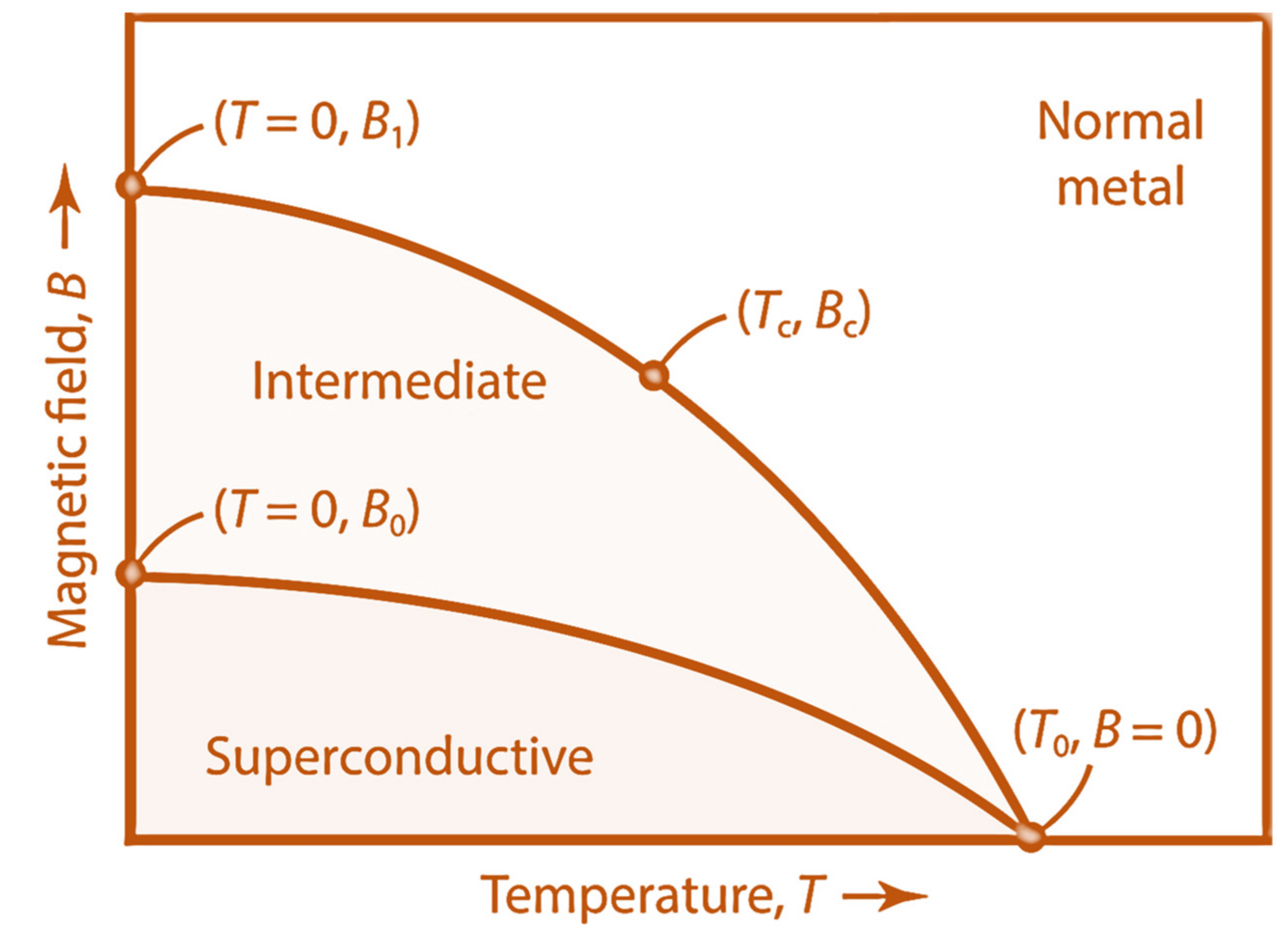
- Hc—critical magnetic field;
- Λm—thickness of the layer.
1.1. Theories of Superconductivity
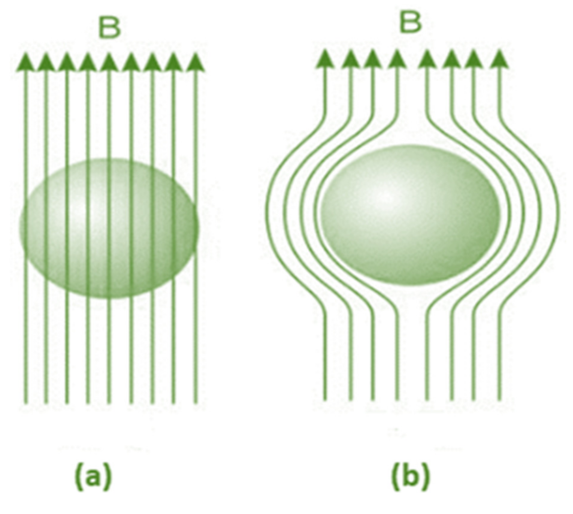
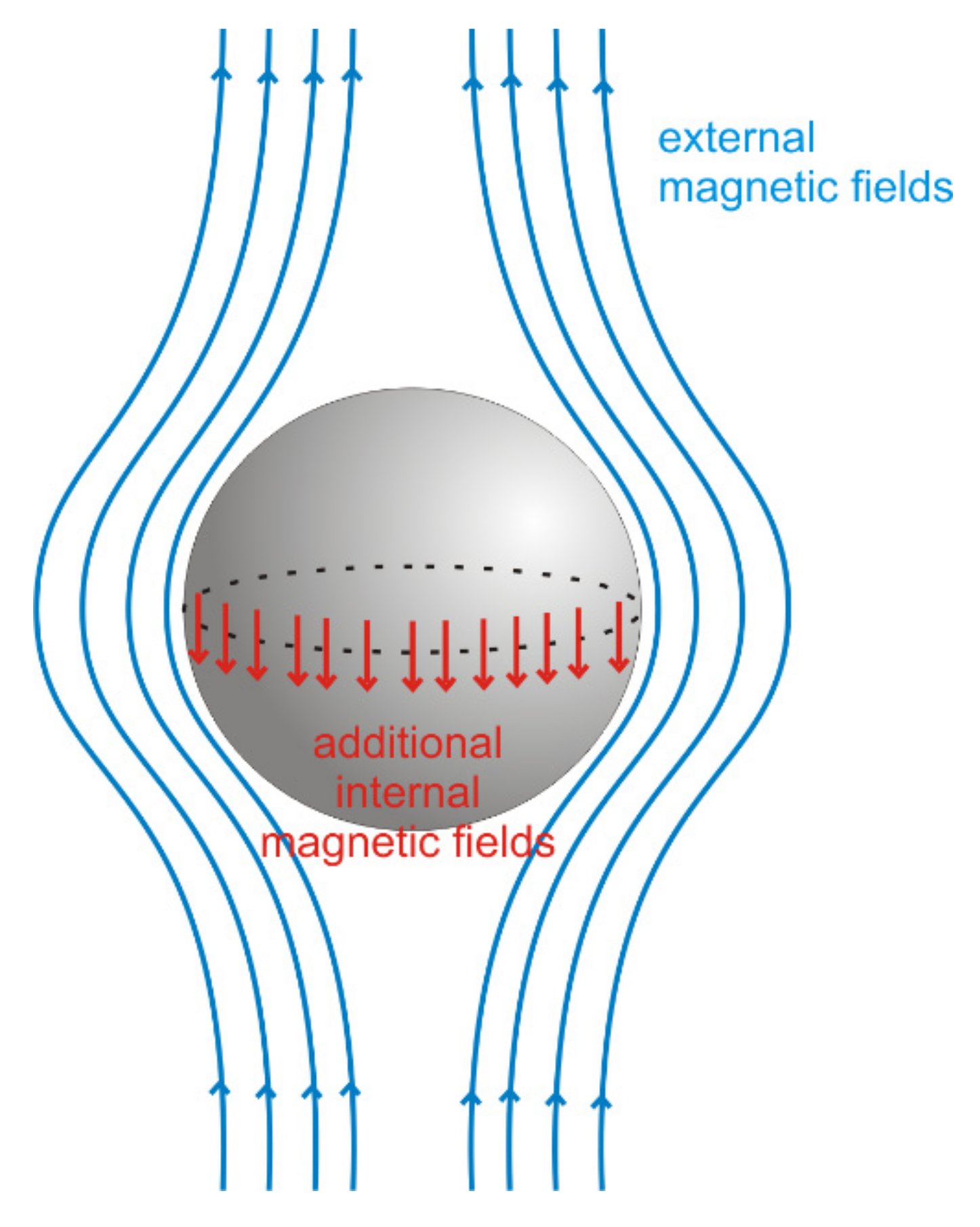
1.1.1. London Theory
- m—mass of charge carrier;
- e—charge;
- n—density of the charge carriers;
- J—current density.
- v—drift velocity of electrons;
- E—electric field.
- i.
- It is the simplest theory of superconductivity;
- ii.
- It captures the Meissner Effect and calculates the surface screening super currents;
- iii.
- Receives only a single parameter, either λL or n;
- iv.
- Numerical complexity comparable to that of Maxwell;
- v.
- Linear equations, so there’s good convergence prospects.
- i.
- Classical only, and has no quantum basis, therefore no treatment of secondary effects;
- ii.
- Valid only in homogeneous materials;
- iii.
- Cannot handle intermediate states, where different regions of the same material can be in different states of superconductivity, and formation of domains;
- iv.
- It is a local theory and does not capture non local effect.
1.1.2. Ginzburg–Landau Theory
- Fn—free energy in the normal phase;
- α, β—phenomenological parameters;
- q—2e for cooper pair;
- A—electromagnetic vector potential;
- B—the magnetic field strength;
- µ0—magnetic permeability in a vacuum.
- Js—is the superconducting electrical current density.
1.1.3. BCS (Barden, Cooper, and Schrieffer) Theory
- Δ—is the energy gap;
- ωD—is the Deby frequency;
- n—density of state of electrons at the fermi energy level EF;
- V—electron phonon coupling constant.
- i.
- The electronic specific heat of a superconductor at very low temperatures (close to 0 K);
- ii.
- Ultrasonic absorption below Tc;
- iii.
- Microwave/far infrared transmission in superconducting thin films and by tunnelling of electrons under I–V characteristics.
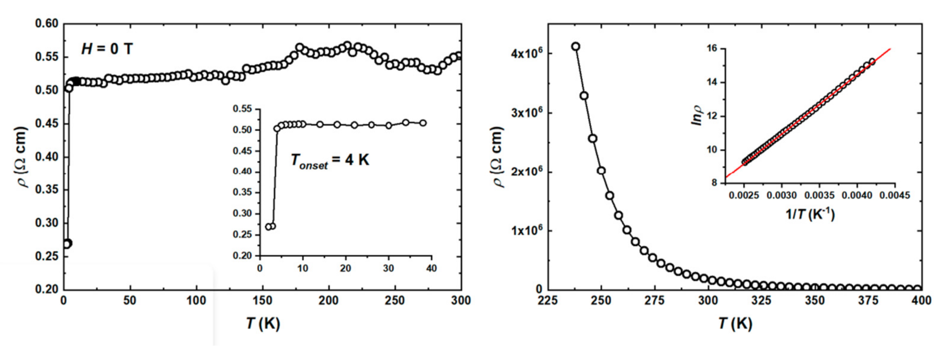
2. Thin Film Superconductors
2.1. Fe-Based Thin-Film Superconductors
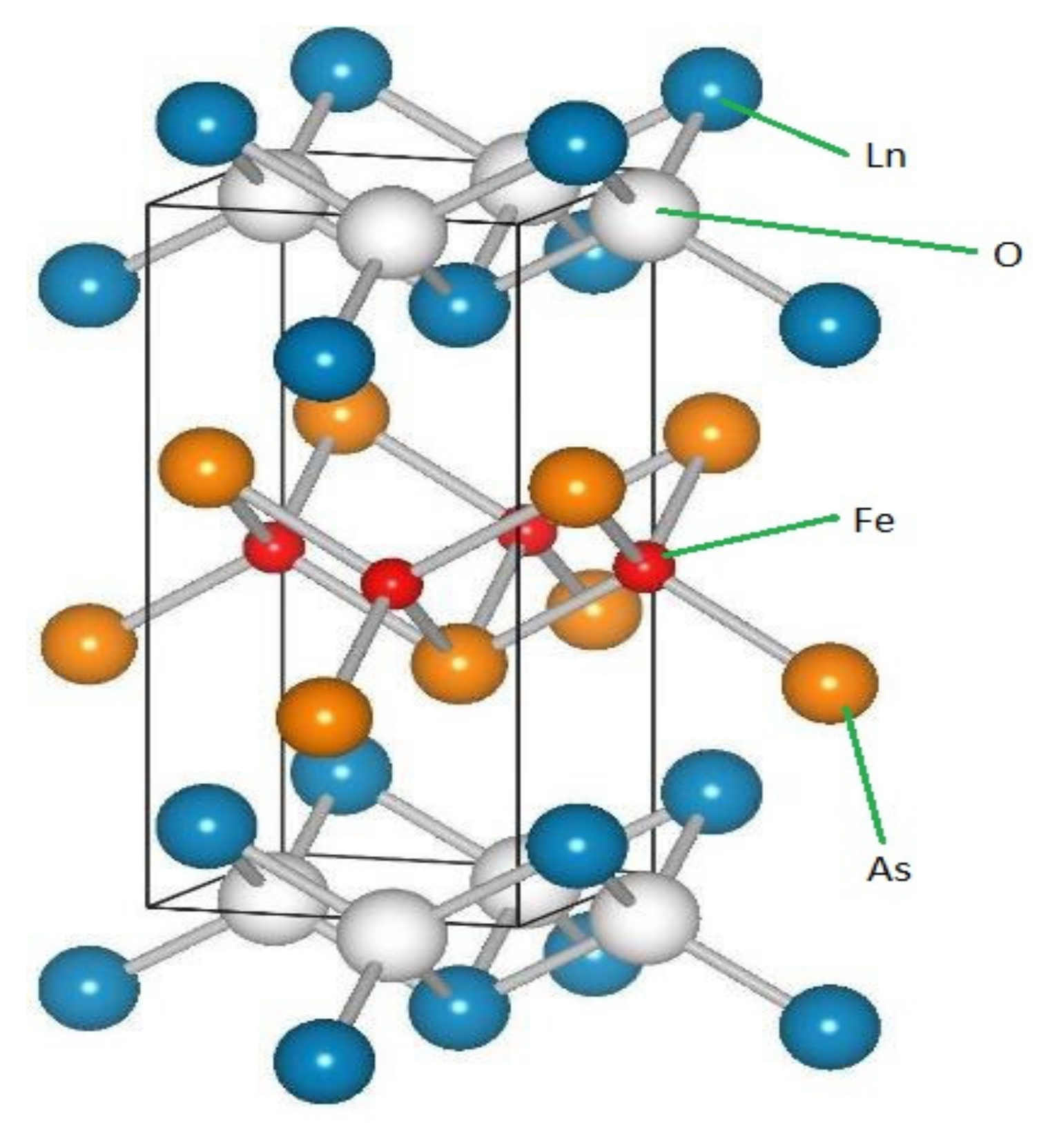
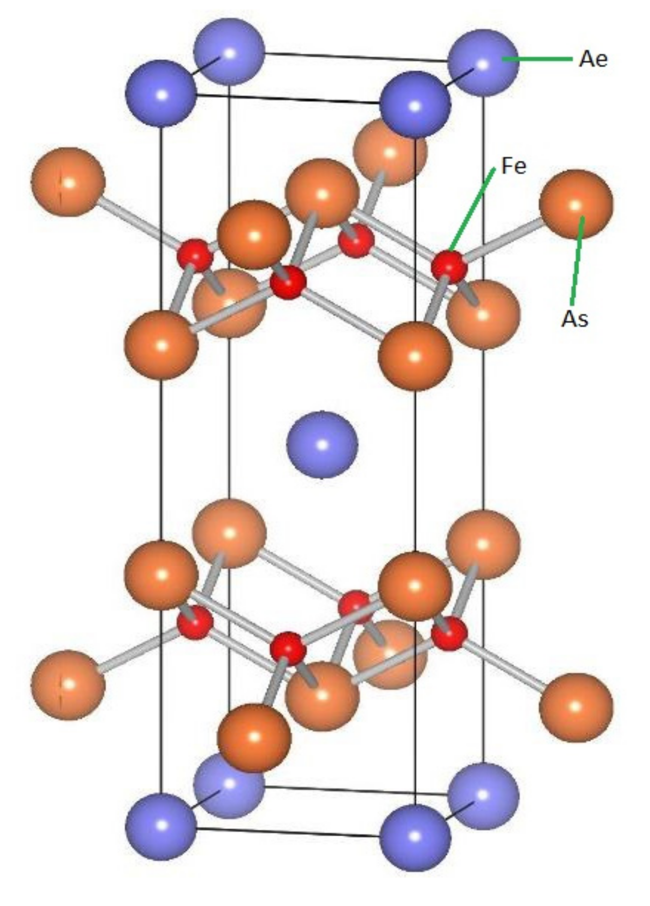
2.1.1. LnFeAs(O,F) Family
2.1.2. Doped AeFe2As2 family
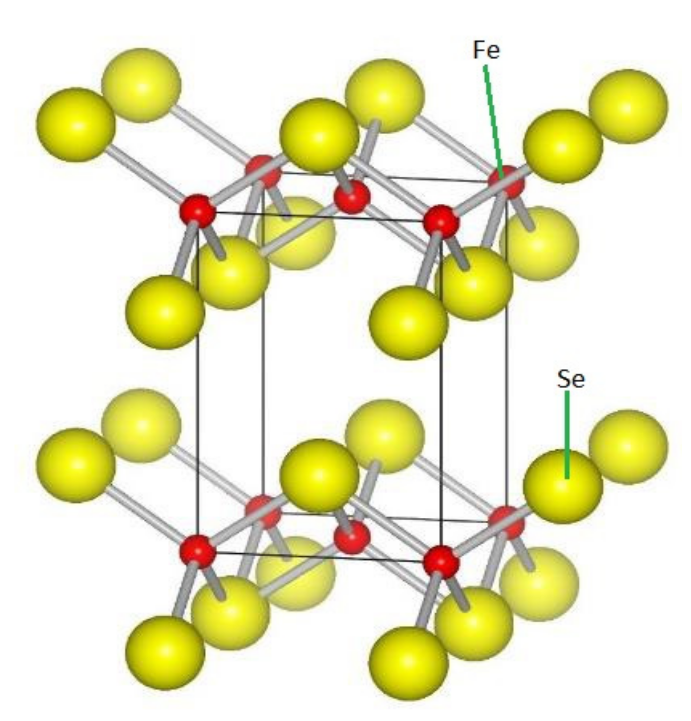
2.1.3. FeCh and FeSe Mono-Layer Film Family
2.2. Layered Titanium Compounds
2.3. Intercalation Compounds with Layered and Cage-like Structures
2.4. Other Superconductors
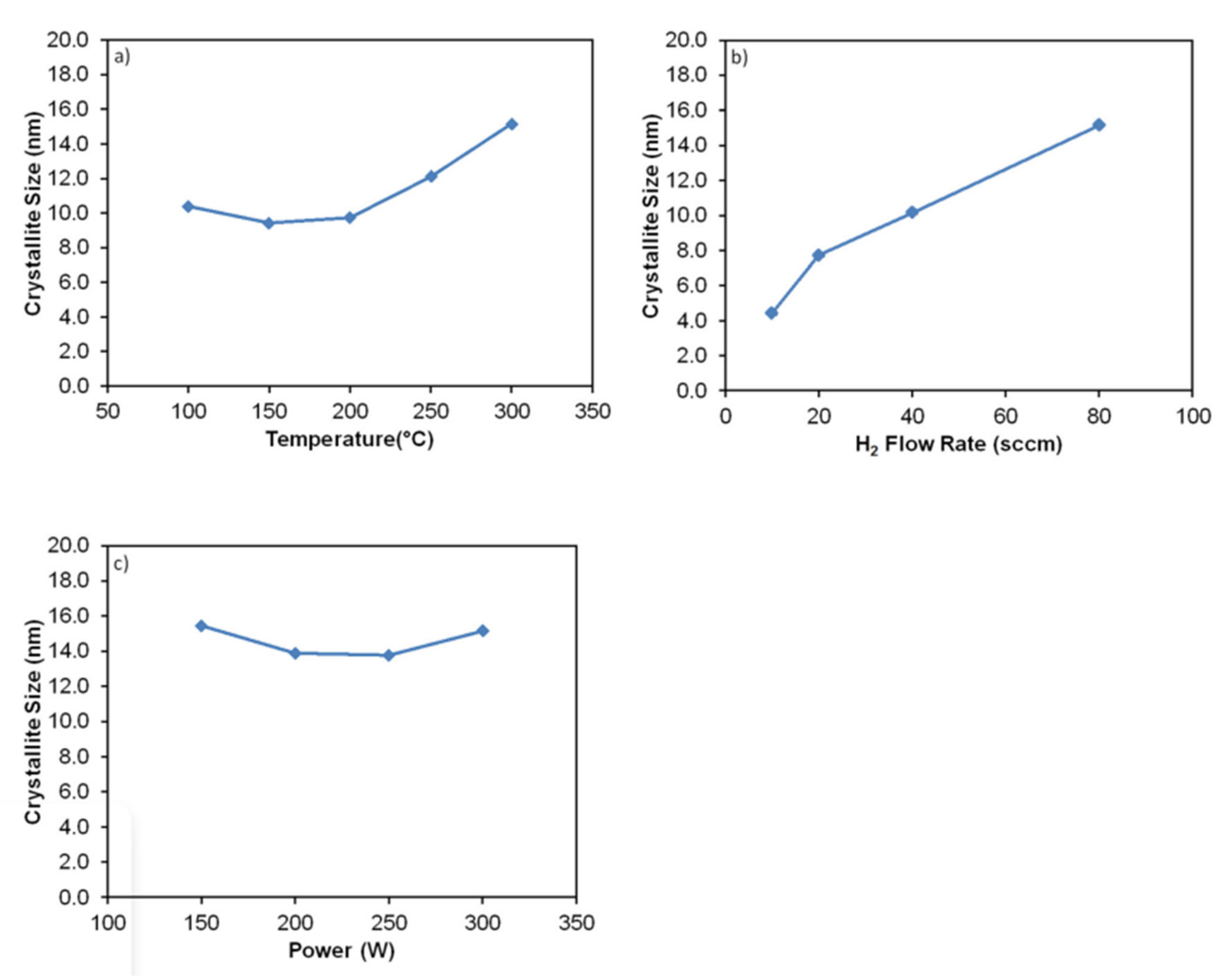
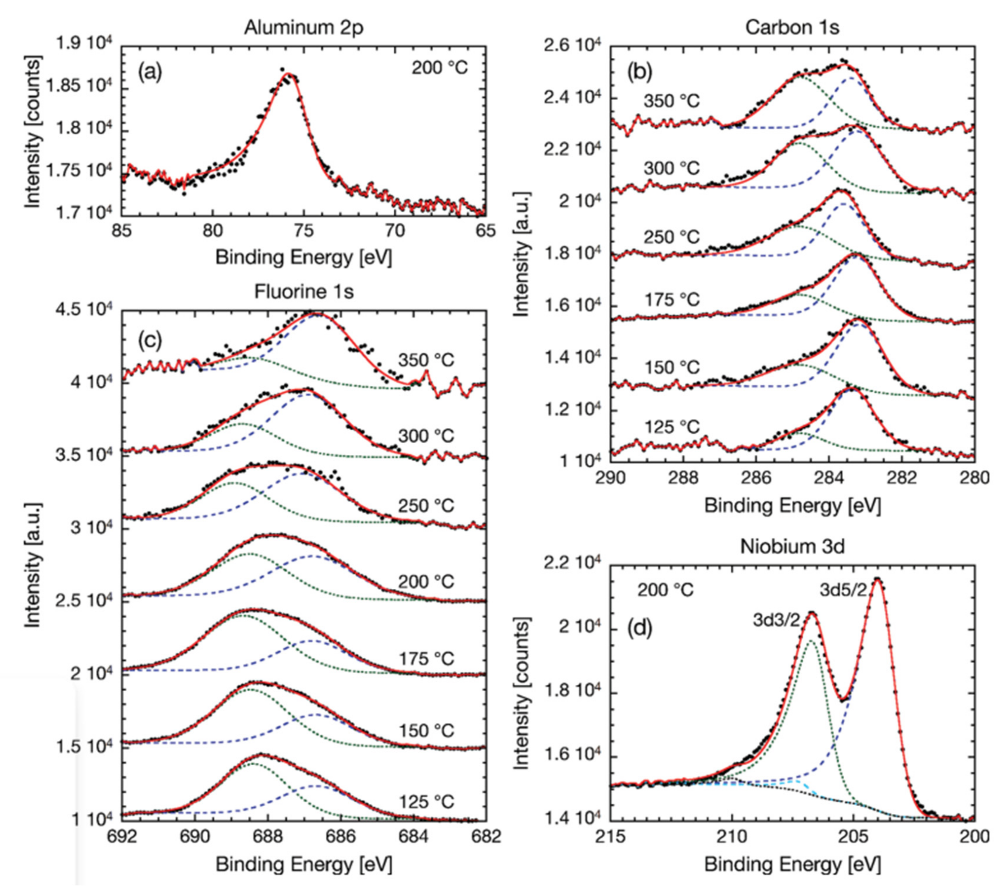
3. Atomic Layer Deposition in the Synthesis of Thin Film Superconductors
4. Current and Future Applications of Superconductors
5. Superconductor Technology Challenges
6. Conclusions
Author Contributions
Funding
Acknowledgments
Conflicts of Interest
References
- Hott, R.; Kleiner, R.; Wolf, T.; Zwicknagl, G. Review on Superconducting Materials. Arxiv Prepr. 2013, arXiv:1306.0429. [Google Scholar] [CrossRef]
- Cuo, L.A.; Green, B. Superconducting Phases in Bulk and Thin Film LA2 CuO4. Undergrad. Rev. 2008, 4, 85–92. [Google Scholar]
- Ruan, B.-B.; Zhao, K.; Mu, Q.-G.; Pan, B.-J.; Liu, T.; Yang, H.-X.; Li, J.-Q.; Chen, G.-F.; Ren, Z.-A. Superconductivity in Bi3O2S2Cl with Bi–Cl Planar Layers. J. Am. Chem. Soc. 2019, 141, 3404–3408. [Google Scholar] [CrossRef] [PubMed]
- Asaba, T.; Wang, Y.; Li, G.; Xiang, Z.; Tinsman, C.; Chen, L.; Zhou, S.; Zhao, S.; Laleyan, D.; Li, Y.; et al. Magnetic Field Enhanced Superconductivity in Epitaxial Thin Film WTe2. Sci. Rep. 2018, 8, 6520. [Google Scholar] [CrossRef] [PubMed]
- Bennernann, K.H.; Ketterson, J. The Physics of Superconductors: Conventional and High-Tc Superconductors; Springer: Berlin/Heidelberg, Germany, 2003. [Google Scholar]
- Lundy, D.R.; Swartzendruber, L.J.; Bennett, L. A BriefReview of Recent Superconductivity Research at NIST. J. Res. Natl. Inst. Stand Technol. 1989, 94, 147–174. [Google Scholar] [CrossRef] [PubMed]
- Bardeen, J.; Cooper, L.N.; Schrieffer, J. Theory of Superconductivity. J. Phys. 1957, 108, 1175–1204. [Google Scholar] [CrossRef]
- London, F.; London, H. The electromagnetic equations of the supraconductor. Proc. Roy. Soc. 1934, 85, 71–88. [Google Scholar]
- Kogan, V.; Nakagawa, N. Moving Pearl Vortices in Thin-Film Superconductors. Condens. Matter 2021, 6, 4. [Google Scholar] [CrossRef]
- Gelens, L.; Matías, M.A.; Gomila, D.; Dorissen, T.; Colet, P. Formation of localized structures in bistable systems through nonlocal spatial coupling. II. the nonlocal Ginzburg-Landau equation. Phys. Rev. E 2014, 89, 012915. [Google Scholar] [CrossRef]
- Ginzburg, V.L.; Landau, L.D. On the Theory of superconductivity. Zh. Eksperim. Teor. Fiz. 1950, 20, 1064–1082. [Google Scholar]
- Flores-Livas, J.A.; Boeri, L.; Sanna, A.; Profeta, G.; Arita, R.; Eremets, M. A perspective on conventional high-temperature superconductors at high pressure: Methods and materials. Phys. Rep. 2020, 856, 1–78. [Google Scholar] [CrossRef]
- Bennemann, K.H.; Ketterson, J. The Physics of Superconductors: Superconductivity in Nanostructures, High-Tc and Novel Superconductors, Organic Superconductors; Springer: Berlin/Heidelberg, Germany, 2004. [Google Scholar]
- Jha, A.K.; Matsumoto, K. Superconductive REBCO Thin Films and Their Nanocomposites: The Role of Rare-Earth Oxides in Promoting Sustainable Energy. Front. Phys. 2019, 7, 1–21. [Google Scholar] [CrossRef]
- Zhang, C.; Hao, F.; Gao, G.; Liu, X.; Ma, C.; Lin, Y.; Yin, Y.; Li, X. Enhanced superconductivity in TiO epitaxial thin films. npj Quantum Mater. 2017, 2, 2. [Google Scholar] [CrossRef]
- Agafonov, A.I. Finding the boson-number distributions in superconducting thin-film rings. Int. J. Mod. Phys. B 2014, 28, 1–15. [Google Scholar] [CrossRef]
- Vestgården, J.I.; Johansen, T.H.; Galperin, Y.M. Nucleation and propagation of thermomagnetic avalanches in thin-film superconductors (Review Article). Low Temp. Phys. 2018, 44, 460–476. [Google Scholar] [CrossRef]
- Antoine, C.Z.; Berry, S.; Bouat, S.; Jacquot, J.-F.; Villégier, J.-C.; Lamura, G.; Gurevich, A. Characterization of superconducting nanometric multilayer samples for superconducting rf applications: First evidence of magnetic screening effect. Phys. Rev. Spéc. Top. Accel. Beams 2010, 13, 121001. [Google Scholar] [CrossRef]
- Stewart, G.R. Unconventional superconductivity. Adv. Phys. 2017, 66, 75–196. [Google Scholar] [CrossRef]
- Fernandes, R.M.; Conde-Gallardo, A.; Ayón-Beato, E.; Godina-Nava, J.J.; Hernández-Contreras, M.; Velasco-Sevilla, L. Conventional and unconventional superconductivity. AIP Conf. Proc. 2012, 1420, 135–144. [Google Scholar] [CrossRef]
- Sakoda, M.; Iida, K.; Naito, M. Recent progress in thin-film growth of Fe-based superconductors: Superior superconductivity achieved by thin films. Supercond. Sci. Technol. 2018, 31, 093001. [Google Scholar] [CrossRef]
- Huebener, R. Conductors, Semiconductors and Superconductors: An Introduction to Solid State Physics, 2nd ed.; Springer International Publishing: Cham, Switzerland, 2016. [Google Scholar]
- Zhi-An, R.; Wei, L.; Jie, Y.; Wei, Y.; Xiao-Li, S.; Zheng, C. Superconductivity at 55 K in Iron-Based F-Doped Layered Quaternary Compound SmFeAs. Chin. Phys. Lett. 2008, 25, 2215. [Google Scholar] [CrossRef]
- Watanabe, T.; Yanagi, H.; Kamihara, Y.; Kamiya, T.; Hirano, M.; Hosono, H. Nickel-based layered superconductor, LaNiOAs. J. Solid State Chem. 2008, 181, 2117–2120. [Google Scholar] [CrossRef]
- Nobukane, H.; Yanagihara, K.; Kunisada, Y.; Ogasawara, Y.; Isono, K.; Nomura, K.; Tanahashi, K.; Nomura, T.; Akiyama, T.; Tanda, S. Co-appearance of superconductivity and ferromagnetism in a Ca2RuO4 nanofilm crystal. Sci. Rep. 2020, 10, 3462. [Google Scholar] [CrossRef]
- Watanabe, T.; Yanagi, H.; Kamiya, T.; Kamihara, Y.; Hiramatsu, H.; Hirano, M.; Hosono, H. Nickel-Based Oxyphosphide Superconductor with a Layered Crystal Structure, LaNiOP. Inorg. Chem. 2007, 46, 7719–7721. [Google Scholar] [CrossRef] [PubMed]
- Gorter, C.J. Superconductivity I. Physica 1949, 15, 55–64. [Google Scholar] [CrossRef]
- Camacho, W.Y.C.; Da Silva, R.M.; Shanenko, A.; Vagov, A.; Vasenko, A.S.; Lvov, B.; Aguiar, J.A.; Cordoba, W.Y. Spontaneous pattern formation in superconducting films. J. Phys. Condens. Matter 2019, 32, 075403. [Google Scholar] [CrossRef] [PubMed]
- Miikkulainen, V.; Leskela, M.; Ritala, M.; Puurunen, R.L. Crystallinity of inorganic films grown by atomic layer deposition: Overview and general trends. J. Appl. Phys. 2013, 113, 021301. [Google Scholar] [CrossRef]
- Hazra, D.; Tsavdaris, N.; Jebari, S.; Grimm, A.; Blanchet, F.; Mercier, F.; Blanquet, E.; Chapelier, C.; Hofheinz, M. Superconducting properties of very high quality NbN thin films grown by high temperature chemical vapor deposition. Supercond. Sci. Technol. 2016, 29, 105011. [Google Scholar] [CrossRef]
- Keskiväli, L.; Putkonen, M.; Puhakka, E.; Kenttä, E.; Kint, J.; Ramachandran, R.K.; Detavernier, C.; Simell, P. Molecular Layer Deposition Using Ring-Opening Reactions: Molecular Modeling of the Film Growth and the Effects of Hydrogen Peroxide. ACS Omega 2018, 3, 7141–7149. [Google Scholar] [CrossRef]
- Hinz, J.; Bauer, A.J.; Frey, L. Analysis of NbN thin film deposition by plasma-enhanced ALD for gate electrode application. Semicond. Sci. Technol. 2010, 25, 075009. [Google Scholar] [CrossRef]
- Ashcroft, N.W.; Mermin, N.D. Solid State Physics; Holt, Rinehart and Winston, University of California: Los Angeles, CA, USA, 1976. [Google Scholar]
- Ohring, M. Materials Science of Thin Films: Deposition and Structure; Academic Press: Cambridge, MA, USA, 2002. [Google Scholar]
- Luth, H. Solid Surfaces, Interfaces and Thin Films; Springer: New York, NY, USA, 2015. [Google Scholar]
- Ruf, J.P.; Paik, H.; Schreiber, N.J.; Nair, H.P.; Miao, L.; Kawasaki, J.K.; Nelson, J.N.; Faeth, B.D.; Lee, Y.; Goodge, B.H.; et al. Strain-stabilized superconductivity. Nat. Commun. 2021, 12, 59. [Google Scholar] [CrossRef]
- Brun, C.; Cren, T.; Roditchev, D. Review of 2D superconductivity: The ultimate case of epitaxial monolayers. Supercond. Sci. Technol. 2016, 30, 013003. [Google Scholar] [CrossRef]
- Fabian, M.D.; Shpiro, B.; Rabani, E.; Neuhauser, D.; Baer, R. Stochastic density functional theory. WIREs Comput. Mol. Sci. 2019, 9, 1–15. [Google Scholar] [CrossRef]
- Klein, O. Theory of Superconductivity. Nature 1952, 169, 578–579. [Google Scholar] [CrossRef]
- Zhou, K.; Wang, J.; Song, Y.; Guo, L.; Guo, J. Highly-Tunable Crystal Structure and Physical Properties in FeSe-Based Superconductors. Crystal 2019, 9, 560. [Google Scholar] [CrossRef]
- Cho, Y.; Kim, S.H.; Kim, B.S.; Kim, Y.; Jeon, W. Modulation of the adsorption chemistry of a precursor in atomic layer deposition to enhance the growth per cycle of a TiO2 thin film. Phys. Chem. Chem. Phys. 2021, 23, 2568–2574. [Google Scholar] [CrossRef] [PubMed]
- Mohlala, L.M.; Jen, T.-C.; Olubambi, P.A. Thermal stability and reactivity of titanium halide precursors for the atomic layer deposition of TiO2 on a Pt (111) surface. Procedia CIRP 2020, 93, 9–13. [Google Scholar] [CrossRef]
- Imai, Y.; Nabeshima, F.; Maeda, A. Comparative Review on Thin Film Growth of Iron-Based Superconductors. Condens. Matter 2017, 2, 25. [Google Scholar] [CrossRef]
- Kamihara, Y.; Watanabe, T.; Hirano, M.; Hosono, H. Iron-Based Layered Superconductor La[O1−xFx]FeAs (x = 0.05 − 0.12) with Tc = 26 K. J. Am. Chem. Soc. 2008, 130, 3296–3297. [Google Scholar] [CrossRef]
- Iida, K.; Hänisch, J.; Tarantini, C. Fe-based superconducting thin films on metallic substrates: Growth, characteristics, and relevant properties. Appl. Phys. Rev. 2018, 5, 031304. [Google Scholar] [CrossRef]
- Virtanen, P.; Braggio, A.; Giazotto, F. Superconducting size effect in thin films under electric field: Mean-field self-consistent model. Phys. Rev. B 2019, 100, 224506. [Google Scholar] [CrossRef]
- Hiramatsu, H.; Kamiya, T.; Hirano, M.; Hosono, H. Heteroepitaxial film growth of layered compounds with the ZrCuSiAs-type and ThCr2Si2-type structures: From Cu-based semiconductors to Fe-based superconductors. Phys. C Supercond. 2009, 469, 657–666. [Google Scholar] [CrossRef]
- Hiramatsu, H.; Katase, T.; Kamiya, T.; Hosono, H. Thin Film Growth and Device Fabrication of Iron-Based Superconductors. J. Phys. Soc. Jpn. 2012, 81, 1–25. [Google Scholar] [CrossRef]
- Tanabe, K.; Hosono, H. Frontiers of Research on Iron-Based Superconductors toward Their Application. Jpn. J. Appl. Phys. 2011, 51, 10005. [Google Scholar] [CrossRef]
- Mele, P. Superconducting properties of iron chalcogenide thin films. Sci. Technol. Adv. Mater. 2012, 13, 054301. [Google Scholar] [CrossRef] [PubMed]
- Haindl, S.; Kidszun, M.; Oswald, S.; Hess, C.; Büchner, B.; Kölling, S.; Wilde, L.; Thersleff, T.; Yurchenko, V.V.; Jourdan, M.; et al. Thin film growth of Fe-based superconductors: From fundamental properties to functional devices. A comparative review. Rep. Prog. Phys. 2014, 77, 046502. [Google Scholar] [CrossRef]
- Sadovskii, M.V. High-temperature superconductivity in monolayers FeSe. Uspekhi Fiz. Nauk 2016, 186, 1035–1057. [Google Scholar] [CrossRef]
- Hosono, H.; Yamamoto, A.; Hiramatsu, H.; Ma, Y. Recent advances in iron-based superconductors toward applications. Mater. Today 2018, 21, 278–302. [Google Scholar] [CrossRef]
- Hosono, H.; Tanabe, K.; Takayama-Muromachi, E.; Kageyama, H.; Yamanaka, S.; Kumakura, H.; Nohara, M.; Hiramatsu, H.; Fujitsu, S. Exploration of new superconductors and functional materials, and fabrication of superconducting tapes and wires of iron pnictides. Sci. Technol. Adv. Mater. 2015, 16, 033503. [Google Scholar] [CrossRef]
- Hsu, F.-C.; Luo, J.-Y.; Yeh, K.-W.; Chen, T.-K.; Huang, T.-W.; Wu, P.M.; Lee, Y.-C.; Huang, Y.-L.; Chu, Y.-Y.; Yan, D.-C.; et al. Superconductivity in the PbO-type structure α-FeSe. Proc. Natl. Acad. Sci. USA 2008, 105, 14262–14264. [Google Scholar] [CrossRef]
- Kamihara, Y.; Hiramatsu, H.; Hirano, M.; Kawamura, R.; Yanagi, H.; Kamiya, T.; Hosono, H. Iron-Based Layered Superconductor: LaOFeP. J. Am. Chem. Soc. 2006, 128, 10012–10013. [Google Scholar] [CrossRef]
- Ren, Z.-A.; Che, G.-C.; Dong, X.-L.; Yang, J.; Lu, W.; Yi, W.; Shen, X.-L.; Li, Z.-C.; Sun, L.-L.; Zhou, F.; et al. Superconductivity and phase diagram in iron-based arsenic-oxides ReFeAsO 1−δ (Re = rare-earth metal) without fluorine doping. Eur. Lett. 2008, 83, 17002. [Google Scholar] [CrossRef]
- Kawaguchi, T.; Uemura, H.; Ohno, T.; Watanabe, R.; Tabuchi, M.; Ujihara, T.; Takenaka, K.; Takeda, Y.; Ikuta, H. Epitaxial Growth of NdFeAsO Thin Films by Molecular Beam Epitaxy. Appl. Phys. Express 2009, 2, 093002. [Google Scholar] [CrossRef]
- Kawaguchi, T.; Uemura, H.; Ohno, T.; Tabuchi, M.; Ujihara, T.; Takenaka, K.; Takeda, Y.; Ikuta, H. In situ growth of superconducting NdFeAs(O,F) thin films by molecular beam epitaxy. Appl. Phys. Lett. 2010, 97, 042509. [Google Scholar] [CrossRef]
- Backen, E.; Haindl, S.; Niemeier, T.; Hühne, R.; Freudenberg, T.; Werner, J.; Behr, G.; Schultz, L.; Holzapfel, B. Growth and anisotropy of La(O, F)FeAs thin films deposited by pulsed laser deposition. Supercond. Sci. Technol. 2008, 21, 122001. [Google Scholar] [CrossRef]
- Kidszun, M.; Haindl, S.; Reich, E.; Hänisch, J.; Iida, K.; Schultz, L.; Holzapfel, B. Epitaxial LaFeAsO1−xFx thin films grown by pulsed laser deposition. Supercond. Sci. Technol. 2010, 23, 022002. [Google Scholar] [CrossRef]
- Ueda, S.; Takeda, S.; Takano, S.; Yamamoto, A.; Naito, M. High-Tc and high-Jc SmFeAs(O,F) films on fluoride substrates grown by molecular beam epitaxy. Appl. Phys. Lett. 2011, 99, 232505. [Google Scholar] [CrossRef]
- Tsukada, I.; Hanawa, M.; Akiike, T.; Nabeshima, F.; Imai, Y.; Ichinose, A.; Komiya, S.; Hikage, T.; Kawaguchi, T.; Ikuta, H.; et al. Epitaxial Growth of FeSe0.5Te0.5Thin Films on CaF2Substrates with High Critical Current Density. Appl. Phys. Express 2011, 4, 053101. [Google Scholar] [CrossRef]
- Haindl, S.; Hanzawa, K.; Sato, H.; Hiramatsu, H.; Hosono, H. In-situ growth of superconducting SmO1−xFxFeAs thin films by pulsed laser deposition. Sci. Rep. 2016, 6, 35797. [Google Scholar] [CrossRef]
- Kamihara, Y.; Nomura, T.; Hirano, M.; Kim, J.E.; Kato, K.; Takata, M.; Kobayashi, Y.; Kitao, S.; Higashitaniguchi, S.; Yoda, Y.; et al. Electronic and magnetic phase diagram of superconductors, SmFeAsO1−xFx. New J. Phys. 2010, 12, 1–14. [Google Scholar] [CrossRef]
- Rotter, M.; Pangerl, M.; Tegel, M.; Johrendt, D. Superconductivity and Crystal Structures of (Ba1−xKx)Fe2As2(x = 0–1). Angew. Chem. Int. Ed. 2008, 47, 7949–7952. [Google Scholar] [CrossRef]
- Rotter, M.; Tegel, M.; Johrendt, D. Superconductivity at 38 K in the Iron Arsenide(Ba1−xKx)Fe2As2. Phys. Rev. Lett. 2008, 101, 107006. [Google Scholar] [CrossRef] [PubMed]
- Lee, N.H.; Jung, S.-G.; Kim, D.H.; Kang, W. Potassium-doped BaFe2As2 superconducting thin films with a transition temperature of 40 K. Appl. Phys. Lett. 2010, 96, 202505. [Google Scholar] [CrossRef]
- Lee, N.H.; Jung, S.-G.; Ranot, M.; Kang, W. Fabrication details of Ba1−xKxFe2As2 films by pulsed laser deposition technique. Prog. Supercond. Cryog. 2014, 16, 4–6. [Google Scholar] [CrossRef][Green Version]
- Agatsuma, S.; Yamagishi, T.; Takeda, S.; Naito, M. MBE growth of FeSe and Sr1−xKxFe2As2. Phys. C 2010, 470, 1468–1472. [Google Scholar] [CrossRef]
- Takeda, S.; Ueda, S.; Yamagishi, T.; Agatsuma, S.; Takano, S.; Mitsuda, A.; Naito, M. Molecular Beam Epitaxy Growth of Superconducting Sr1−xKxFe2As2 and Ba1−xKxFe2As2. Appl. Phys. Express 2010, 3, 093101. [Google Scholar] [CrossRef]
- Ueda, S.; Yamagishi, T.; Takeda, S.; Agatsuma, S.; Takano, S.; Mitsuda, A.; Naito, M. MBE growth of Fe-based superconducting films. Phys. C Supercond. 2011, 471, 1167–1173. [Google Scholar] [CrossRef]
- Yamagishi, T.; Ueda, S.; Takeda, S.; Takano, S.; Mitsuda, A.; Naito, M. A study of the doping dependence of Tc in Ba1−xKxFe2As2 and Sr1−xKxFe2As2 films grown by molecular beam epitaxy. Phys. C Supercond. 2011, 471, 1177–1180. [Google Scholar] [CrossRef]
- Wu, M.K.; Hsu, F.C.; Yeh, K.W.; Huang, T.W.; Luo, J.Y.; Wang, M.J.; Chang, H.H.; Chen, T.K.; Rao, S.M.; Mok, B.H.; et al. The development of the superconducting PbO-type β-FeSe and related compounds. Phys. C 2009, 469, 340–349. [Google Scholar] [CrossRef]
- Yeh, K.-W.; Huang, T.-W.; Huang, Y.-L.; Chen, T.-K.; Hsu, F.-C.; Wu, P.M.; Lee, Y.-C.; Chu, Y.-Y.; Chen, C.-L.; Luo, J.-Y.; et al. Tellurium substitution effect on superconductivity of the α-phase iron selenide. Eur. Lett. 2008, 84, 104502. [Google Scholar] [CrossRef]
- Mizuguchi, Y.; Tomioka, F.; Tsuda, S.; Yamaguchi, T.; Takano, Y. Superconductivity at 27K in tetragonal FeSe under high pressure. Appl. Phys. Lett. 2008, 93, 152505. [Google Scholar] [CrossRef]
- Medvedev, S.; McQueen, T.M.; Troyan, I.A.; Palasyuk, T.; Eremets, M.I.; Cava, R.J.; Naghavi, S.; Casper, F.; Ksenofontov, V.; Wortmann, G.; et al. Electronic and magnetic phase diagram of β-Fe1.01Se with superconductivity at 36.7 K under pressure. Nat. Mater. 2009, 8, 630–633. [Google Scholar] [CrossRef] [PubMed]
- Bellingeri, E.; Kawale, S.; Pallecchi, I.; Gerbi, A.; Buzio, R.; Braccini, V.; Palenzona, A.; Putti, M.; Adamo, M.; Sarnelli, E.; et al. Strong vortex pinning in FeSe0.5Te0.5 epitaxial thin film. Appl. Phys. Lett. 2012, 100, 082601. [Google Scholar] [CrossRef]
- Hanzawa, K.; Sato, H.; Hiramatsu, H.; Kamiya, T.; Hosono, H. Electric field-induced superconducting transition of insulating FeSe thin film at 35 K. Proc. Natl. Acad. Sci. USA 2016, 113, 3986–3990. [Google Scholar] [CrossRef]
- Lei, B.; Cui, J.H.; Xiang, Z.J.; Shang, C.; Wang, N.Z.; Ye, G.J.; Luo, X.G.; Wu, T.; Sun, Z.; Chen, X.H. Evolution of High-Temperature Superconductivity from a Low-TcPhase Tuned by Carrier Concentration in FeSe Thin Flakes. Phys. Rev. Lett. 2016, 116, 077002. [Google Scholar] [CrossRef] [PubMed]
- Nabeshima, F.; Imai, Y.; Hanawa, M.; Tsukada, I.; Maeda, A. Enhancement of the superconducting transition temperature in FeSe epitaxial thin films by anisotropic compression. Appl. Phys. Lett. 2013, 103, 172602. [Google Scholar] [CrossRef]
- Wang, Q.-Y.; Li, Z.; Zhang, W.-H.; Zhang, Z.-C.; Zhang, J.-S.; Li, W.; Ding, H.; Ou, Y.-B.; Deng, P.; Chang, K.; et al. Interface-Induced High-Temperature Superconductivity in Single Unit-Cell FeSe Films on SrTiO3. Chin. Phys. Lett. 2012, 29, 037402. [Google Scholar] [CrossRef]
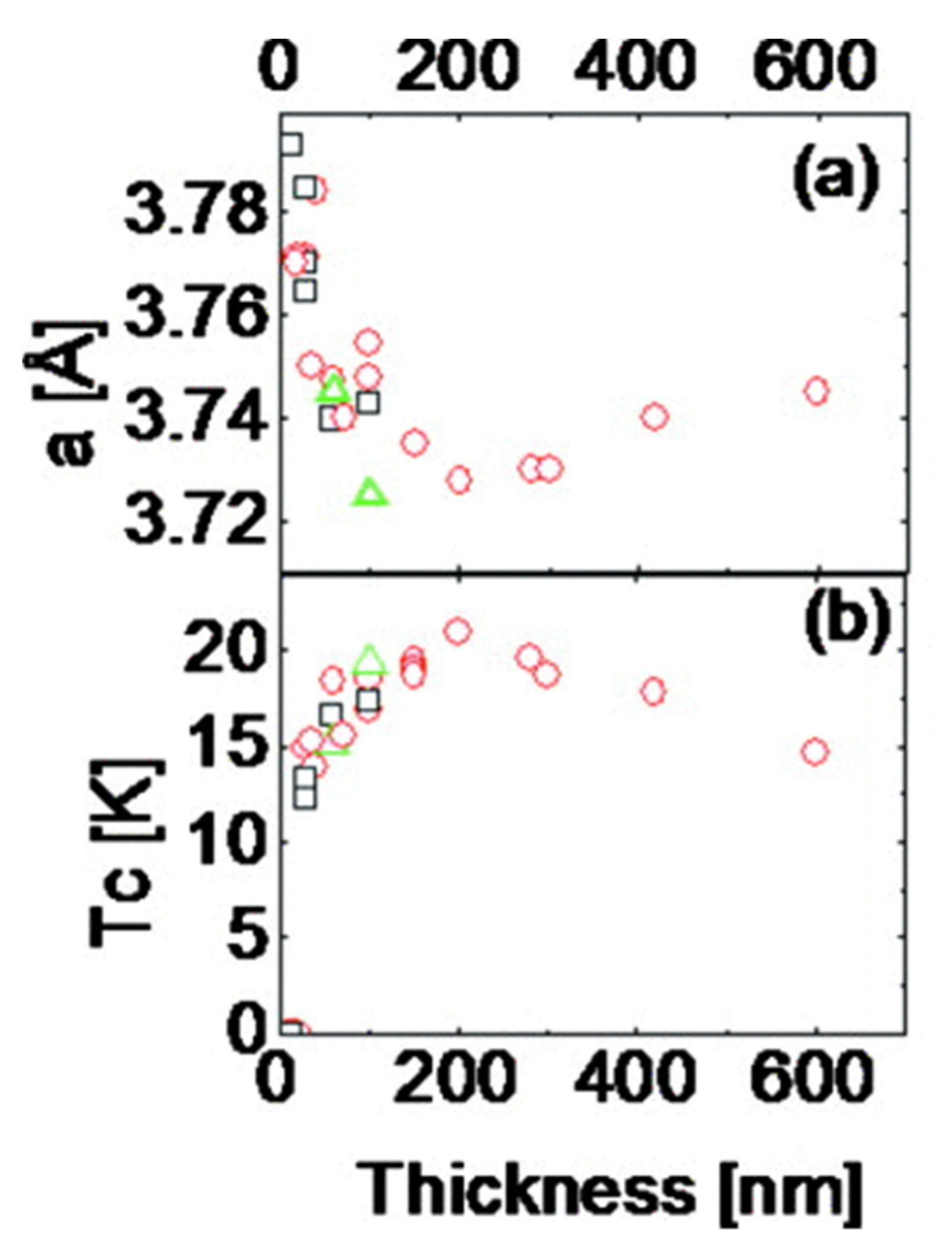
- He, S.; He, J.; Zhang, W.; Zhao, L.; Liu, D.; Liu, X.; Mou, D.; Ou, Y.-B.; Wang, Q.-Y.; Li, Z.; et al. Phase diagram and electronic indication of high-temperature superconductivity at 65 K in single-layer FeSe films. Nat. Mater. 2013, 12, 605–610. [Google Scholar] [CrossRef]
- Ge, J.-F.; Liu, Z.-L.; Liu, C.; Gao, C.-L.; Qian, D.; Xue, Q.-K.; Liu, Y.; Jia, J.-F. Superconductivity above 100 K in single-layer FeSe films on doped SrTiO3. Nat. Mater. 2015, 14, 285–289. [Google Scholar] [CrossRef]
- Putti, M.; Pallecchi, I.; Bellingeri, E.; Cimberle, M.R.; Tropeano, M.; Ferdeghini, C.; Palenzona, A.; Tarantini, C.; Yamamoto, A.; Jiang, J.; et al. New Fe-based superconductors: Properties relevant for applications. Supercond. Sci. Technol. 2010, 23, 034003. [Google Scholar] [CrossRef]
- Imai, Y.; Sawada, Y.; Nabeshima, F.; Maeda, A. Suppression of phase separation and giant enhancement of superconducting transition temperature in FeSe1−x Tex thin films. Proc. Natl. Acad. Sci. USA 2015, 112, 1937–1940. [Google Scholar] [CrossRef]
- Seo, S.; Kang, J.-H.; Oh, M.J.; Jeong, I.-S.; Jiang, J.; Gu, G.; Lee, J.-W.; Lee, J.; Noh, H.; Liu, M.; et al. Origin of the emergence of higher Tc than bulk in iron chalcogenide thin films. Sci. Rep. 2017, 7, 1–8. [Google Scholar] [CrossRef] [PubMed]
- Hanawa, M.; Ichinose, A.; Komiya, S.; Tsukada, I.; Imai, Y.; Maeda, A. Empirical selection rule of substrate materials for iron chalcogenide superconducting thin films. Japan. J. Appl. Phys. 2012, 51, 010104. [Google Scholar] [CrossRef]
- Iida, K.; Hänisch, J.; Schulze, M.; Aswartham, S.; Wurmehl, S.; Büchner, B.; Schultz, L.; Holzapfel, B. Generic Fe buffer layers for Fe-based superconductors: Epitaxial FeSe1−xTex thin films. Appl. Phys. Lett. 2011, 99, 202503. [Google Scholar] [CrossRef]
- Si, W.; Han, S.J.; Shi, X.; Ehrlich, S.N.; Jaroszynski, J.; Goyal, A.; Li, Q. High current superconductivity in FeSe0.5Te0.5-coated conductors at 30 tesla. Nat. Commun. 2013, 4, 1347. [Google Scholar] [CrossRef] [PubMed]
- Ozaki, T.; Wu, L.; Zhang, C.; Jaroszynski, J.; Si, W.; Zhou, J.; Zhu, Y.; Li, Q. A route for a strong increase of critical current in nanostrained iron-based superconductors. Nat. Commun. 2016, 7, 13036. [Google Scholar] [CrossRef]
- Molatta, S.; Haindl, S.; Trommler, S.; Schulze, M.; Wurmehl, S.; Hühne, R. Interface control by homoepitaxial growth in pulsed laser deposited iron chalcogenide thin films. Sci. Rep. 2015, 5, 16334. [Google Scholar] [CrossRef]
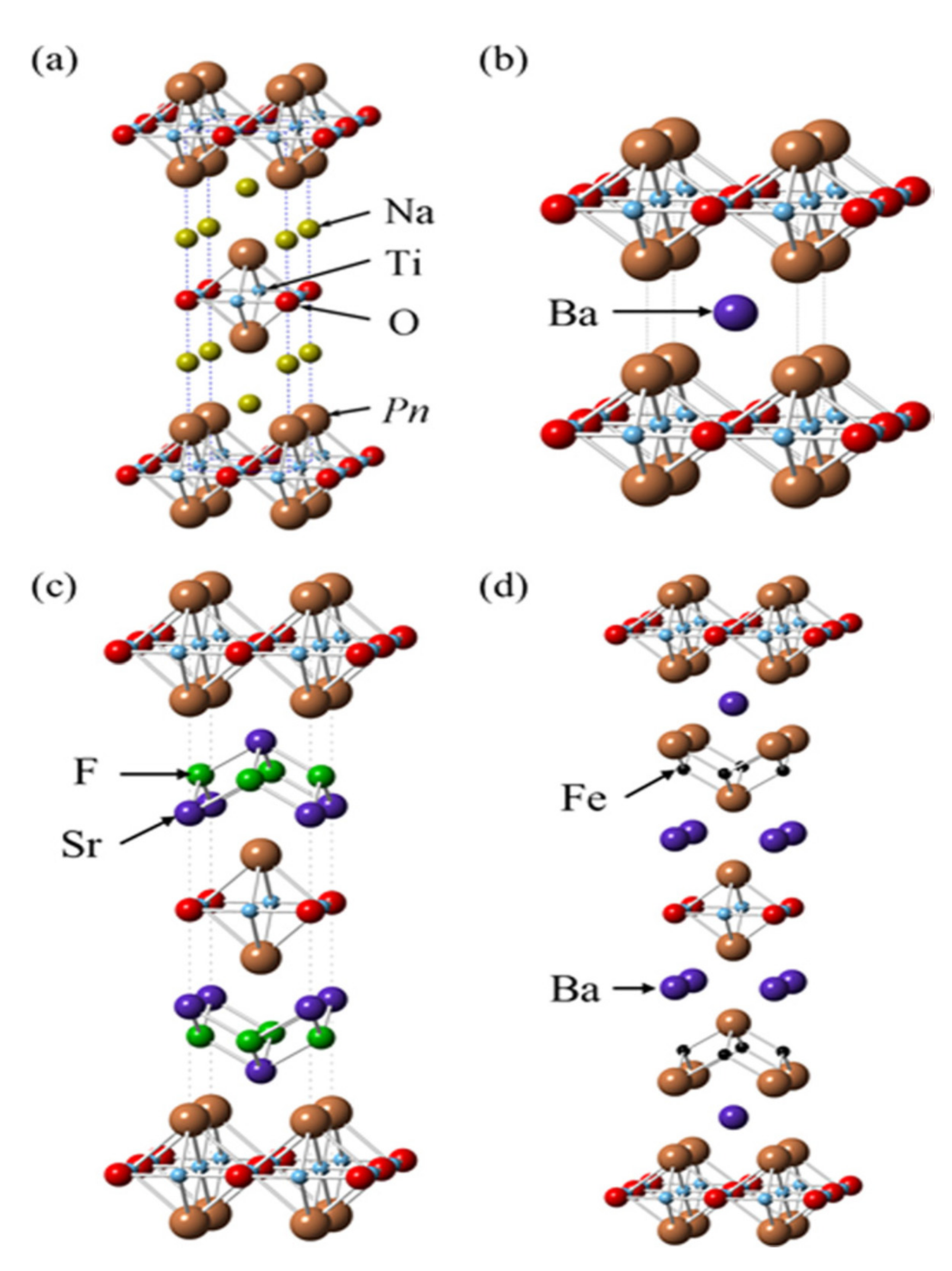
- Ozawa, T.C.; Kauzlarich, S.M.; Bieringer, M.; Greedan, J.E. Possible Charge-Density-Wave/Spin-Density-Wave in the Layered Pnictide−Oxides: Na2Ti2Pn2O (Pn = As, Sb). Chem. Mater. 2001, 13, 1804–1810. [Google Scholar] [CrossRef]
- Liu, R.H.; Tan, D.; Song, Y.A.; Li, Q.J.; Yan, Y.J.; Ying, J.J.; Xie, Y.L.; Wang, X.F.; Chen, X.H. Physical properties of the layered pnictide oxidesNa2Ti2P2O (P = As,Sb). Phys. Rev. B 2009, 80, 144516. [Google Scholar] [CrossRef]
- Lorenz, B.; Guloy, A.M.; Chu, P.C.W. Superconductivity in titanium-based pnictide oxide compounds. Int. J. Mod. Phys. B 2014, 28, 1–25. [Google Scholar] [CrossRef]
- Yajima, T.; Nakano, K.; Takeiri, F.; Ono, T.; Hosokoshi, Y.; Matsushita, Y.; Hester, J.; Kobayashi, Y.; Kageyama, H. Superconductivity in BaTi2Sb2O with ad1Square Lattice. J. Phys. Soc. Jpn. 2012, 81, 1–4. [Google Scholar] [CrossRef]
- Doan, P.; Gooch, M.; Tang, Z.; Lorenz, B.; Möller, A.; Tapp, J.; Chu, P.C.W.; Guloy, A.M. Ba1−xNaxTi2Sb2O (0.0 ≤ x ≤ 0.33): A Layered Titanium-Based Pnictide Oxide Superconductor. J. Am. Chem. Soc. 2012, 134, 16520–16523. [Google Scholar] [CrossRef] [PubMed]
- Yajima, T. Titanium Pnictide Oxide Superconductors. Condens. Matter 2017, 2, 4. [Google Scholar] [CrossRef]
- Adam, A.; Schuster, H.-U. Darstellung und Kristallstruktur der Pnictidoxide Na2Ti2As2O und Na2Ti2Sb2O. ZAAC 1990, 584, 150–158. [Google Scholar] [CrossRef]
- Wang, X.; Yan, Y.J.; Ying, J.J.; Li, Q.J.; Zhang, M.; Xu, N.; Chen, X.H. Structure and physical properties for a new layered pnictide-oxide: BaTi2As2O. J. Phys. Condens. Matter 2010, 22, 075702. [Google Scholar] [CrossRef]
- Yajima, T.; Nakano, K.; Takeiri, F.; Hester, J.; Yamamoto, T.; Kobayashi, Y.; Tsuji, N.; Kim, J.; Fujiwara, A.; Kageyama, H. Synthesis and physical properties of the new oxybismuthides BaTi2Bi2O and (SrF)2Ti2Bi2O with a d1 square net. J. Phys. Soc. Jpn. 2012, 82, 013703. [Google Scholar] [CrossRef]
- Liu, R.H.; Song, Y.A.; Li, Q.J.; Ying, J.J.; Yan, Y.J.; He, Y.; Chen, X. Structure and Physical Properties of the Layered Pnictide-Oxides: (SrF)2Ti2Pn2O (Pn= As, Sb) and (SmO)2Ti2Sb2O. Chem. Mater. 2010, 22, 1503–1508. [Google Scholar] [CrossRef]
- Singh, D.J. Electronic structure, disconnected Fermi surfaces and antiferromagnetism in the layered pnictide superconductor NaxBa1−xTi2Sb2O. New J. Phys. 2012, 14, 123003. [Google Scholar] [CrossRef]
- Suetin, D.V.; Ivanovskii, A.L. Electronic properties and fermi surface for new Fe-free layered pnictide-oxide superconductor BaTi2Bi2O from first principles. JETP Lett. 2013, 97, 220–225. [Google Scholar] [CrossRef]
- Bussmann-Holder, A.; Keller, H. High-temperature superconductors: Underlying physics and applications. Z. Für Nat. B 2020, 75, 3–14. [Google Scholar] [CrossRef]
- Müller, K.A.; Kool, T.W. Superconductivity. Prop. Perovskites Other Oxides 2010, 193, 545–562. [Google Scholar] [CrossRef]
- Mine, T.; Yanagi, H.; Kamiya, T.; Kamihara, Y.; Hirano, M.; Hosono, H. Nickel-based phosphide superconductor with infinite-layer structure, BaNi2P2. Solid State Commun. 2008, 147, 111–113. [Google Scholar] [CrossRef]
- Laloë, J.-B.; Kim, T.H.; Moodera, J.S. Molecular-Beam Epitaxially Grown MgB2Thin Films and Superconducting Tunnel Junctions. Adv. Condens. Matter Phys. 2011, 2011, 989732. [Google Scholar] [CrossRef]
- Askerzade, I. The upper critical field of thin films of two-band superconductors: An application to MgB2. Mod. Phys. Lett. B 2004, 18, 1525–1531. [Google Scholar] [CrossRef]
- Yamanaka, S.; Enishi, E.; Fukuoka, H.; Yasukawa, M. High-Pressure Synthesis of a New Silicon Clathrate Superconductor, Ba8Si46. Inorg. Chem. 2000, 39, 56–58. [Google Scholar] [CrossRef]
- Yamanaka, S. Intercalation and superconductivity in ternary layer structured metal nitride halides (MNX: M = Ti, Zr, Hf; X = Cl, Br, I). J. Mater. Chem. 2010, 20, 2922–2933. [Google Scholar] [CrossRef]
- Yamanaka, S.; Okumura, H.; Zhu, L. Alkali metal intercalation in layer structured α-HfNBr☆. J. Phys. Chem. Solids 2004, 65, 565–569. [Google Scholar] [CrossRef]
- Kuroki, K. Spin-fluctuation-mediatedd+id′pairing mechanism in dopedβ-MNCl(M = Hf,Zr)superconductors. Phys. Rev. B 2010, 81, 1–7. [Google Scholar] [CrossRef]
- Bill, A.; Morawitz, H.; Kresin, V.Z. Dynamical screening and superconducting state in intercalated layered metallochloronitrides. Phys. Rev. B 2002, 66, 100501. [Google Scholar] [CrossRef]
- Bill, A.; Morawitz, H.; Kresin, V.Z. Electronic collective modes and superconductivity in layered conductors. Phys. Rev. B 2003, 68, 144519. [Google Scholar] [CrossRef]
- Yamanaka, S.; Hotehama, K.-I.; Kawaji, H. Superconductivity at 25.5 K in electron-doped layered hafnium nitride. Nature 1998, 392, 580–582. [Google Scholar] [CrossRef]
- Yamanaka, S.; Kawaji, H.; Hotehama, K.-I.; Ohashi, M. A new layer-structured nitride superconductor. Lithium-intercalatedβ-zirconium nitride chloride, LixZrNCl. Adv. Mater. 1996, 8, 771–774. [Google Scholar] [CrossRef]
- Yamanaka, S.; Izumi, S.; Maekawa, S.; Umemoto, K. Phase diagram of the La–Si binary system under high pressure and the structures of superconducting LaSi5 and LaSi10. J. Solid State Chem. 2009, 182, 1991–2003. [Google Scholar] [CrossRef]
- Yamanaka, S.; Maekawa, S. Structural Evolution of the Binary System Ba-Si under High-pressure and High-temperature Conditions. Z. Für Nat. B 2006, 61, 1493–1499. [Google Scholar] [CrossRef]
- Kurakevych, O.O.; Strobel, T.A.; Kim, D.Y.; Muramatsu, T.; Struzhkin, V.V. Na-Si Clathrates Are High-Pressure Phases: A Melt-Based Route to Control Stoichiometry and Properties. Cryst. Growth Des. 2013, 13, 303–307. [Google Scholar] [CrossRef]
- Zhang, S.; Tanaka, M.; Watanabe, E.; Zhu, H.; Inumaru, K.; Yamanaka, S. Superconductivity of alkali metal intercalated TiNBr with α-type nitride layers. Supercond. Sci. Technol. 2013, 26, 122001. [Google Scholar] [CrossRef]
- Ronning, F.; Bauer, E.D.; Park, T.; Baek, S.-H.; Sakai, H.; Thompson, J.D. Superconductivity and the effects of pressure and structure in single-crystallineSrNi2P2. Phys. Rev. B 2009, 79, 134507. [Google Scholar] [CrossRef]
- Hirai, D.; Takayama, T.; Higashinaka, R.; Aruga-Katori, H.; Takagi, H. Superconductivity in Layered Pnictides BaRh2P2 and BaIr2P2. J. Phys. Soc. Jpn. 2009, 78, 1–4. [Google Scholar] [CrossRef]
- Jeitschko, W.; Glaum, R.; Boonk, L. Superconducting LaRu2P2 and other alkaline earth and rare earth metal ruthenium and osmium phosphides and arsenides with ThCr2Si2 structure. J. Solid State Chem. 1987, 69, 93–100. [Google Scholar] [CrossRef]
- Han, J.-T.; Zhou, J.-S.; Cheng, J.-G.; Goodenough, J.B. A New Pnictide Superconductor without Iron. J. Am. Chem. Soc. 2009, 132, 908–909. [Google Scholar] [CrossRef]
- Bauer, E.; Ronning, F.; Scott, B.; Thompson, J.D. Superconductivity inSrNi2As2single crystals. Phys. Rev. B 2008, 78, 172504. [Google Scholar] [CrossRef]
- Ronning, F.; Kurita, N.; Bauer, E.; Scott, B.; Park, T.; Klimczuk, T.; Movshovich, R.; Thompson, J.D. The first order phase transition and superconductivity in BaNi2As2single crystals. J. Phys. Condens. Matter 2008, 20, 342203. [Google Scholar] [CrossRef]
- Imre, A.; Hellmann, A.; Wenski, G.; Graf, J.; Johrendt, D.; Mewis, A. Inkommensurabel modulierte Kristallstrukturen und Phasenumwandlungen–Die Verbindungen SrPt2As2 und EuPt2As2. Z. Für Anorg. Und Allg. Chem. 2007, 633, 2037–2045. [Google Scholar] [CrossRef]
- Tsutsumi, K.; Takayanagi, S.; Ishikawa, M.; Hirano, T. Superconductivity of Intermetallic Compound CoSi2. J. Phys. Soc. Jpn. 1995, 64, 2237. [Google Scholar] [CrossRef]
- Sefat, A.; McGuire, M.; Jin, R.; Sales, B.C.; Mandrus, D.; Ronning, F.; Bauer, E.; Mozharivskyj, Y. Structure and anisotropic properties ofBaFe2-xNixAs2(x = 0, 1, and 2) single crystals. Phys. Rev. B 2009, 79, 094508. [Google Scholar] [CrossRef]
- Kurita, N.; Ronning, F.; Tokiwa, Y.; Bauer, E.D.; Subedi, A.; Singh, D.J.; Thompson, J.D.; Movshovich, R. Low-Temperature Magnetothermal Transport Investigation of a Ni-Based SuperconductorBaNi2As2: Evidence for Fully Gapped Superconductivity. Phys. Rev. Lett. 2009, 102, 147004. [Google Scholar] [CrossRef]
- Subedi, A.; Singh, D.J. Density functional study ofBaNi2As2: Electronic structure, phonons, and electron-phonon superconductivity. Phys. Rev. B 2008, 78, 132511. [Google Scholar] [CrossRef]
- Shein, I.R.; Ivanovskii, A.L. Electronic and structural properties of low-temperature superconductors and ternary pnictides ANi2Pn2 (A = Sr, BaandPn = P,As). Phys. Rev. B 2009, 79, 054510. [Google Scholar] [CrossRef]
- Kudo, K.; Takasuga, M.; Okamoto, Y.; Hiroi, Z.; Nohara, M. Giant Phonon Softening and Enhancement of Superconductivity by Phosphorus Doping ofBaNi2As2. Phys. Rev. Lett. 2012, 109, 097002. [Google Scholar] [CrossRef]
- Toriyama, T.; Kobori, M.; Konishi, T.; Ohta, Y.; Sugimoto, K.; Kim, J.; Fujiwara, A.; Pyon, S.; Kudo, K.; Nohara, M. Switching of Conducting Planes by Partial Dimer Formation in IrTe2. J. Phys. Soc. Jpn. 2014, 83, 33701. [Google Scholar] [CrossRef]
- Pyon, S.; Kudo, K.; Nohara, M. Emergence of superconductivity near the structural phase boundary in Pt-doped IrTe2 single crystals. Physica C. 2013, 494, 80–84. [Google Scholar] [CrossRef]
- Joseph, B.; Bendele, M.; Simonelli, L.; Maugeri, L.; Pyon, S.; Kudo, K. Local structural displacements across the structural phase transition in IrTe2: Order-disorder of dimers and role of Ir-Te correlations. Phys Rev B. 2013, 88, 3–6. [Google Scholar] [CrossRef]
- Jobic, S.; Evain, M.; Brec, R.; Deniard, P.; Jouanneaux, A.; Rouxel, J. Crystal structure of polymeric pyrite type Ir2Te2. J. Solid State Chem. 1991, 95, 319–326. [Google Scholar] [CrossRef]
- Léger, J.; Pereira, A.; Haines, J.; Jobic, S.; Brec, R. Phase transformations of polymeric CdI2-type IrTe2 under high pressure. J. Phys. Chem. Solids 2000, 61, 27–34. [Google Scholar] [CrossRef]
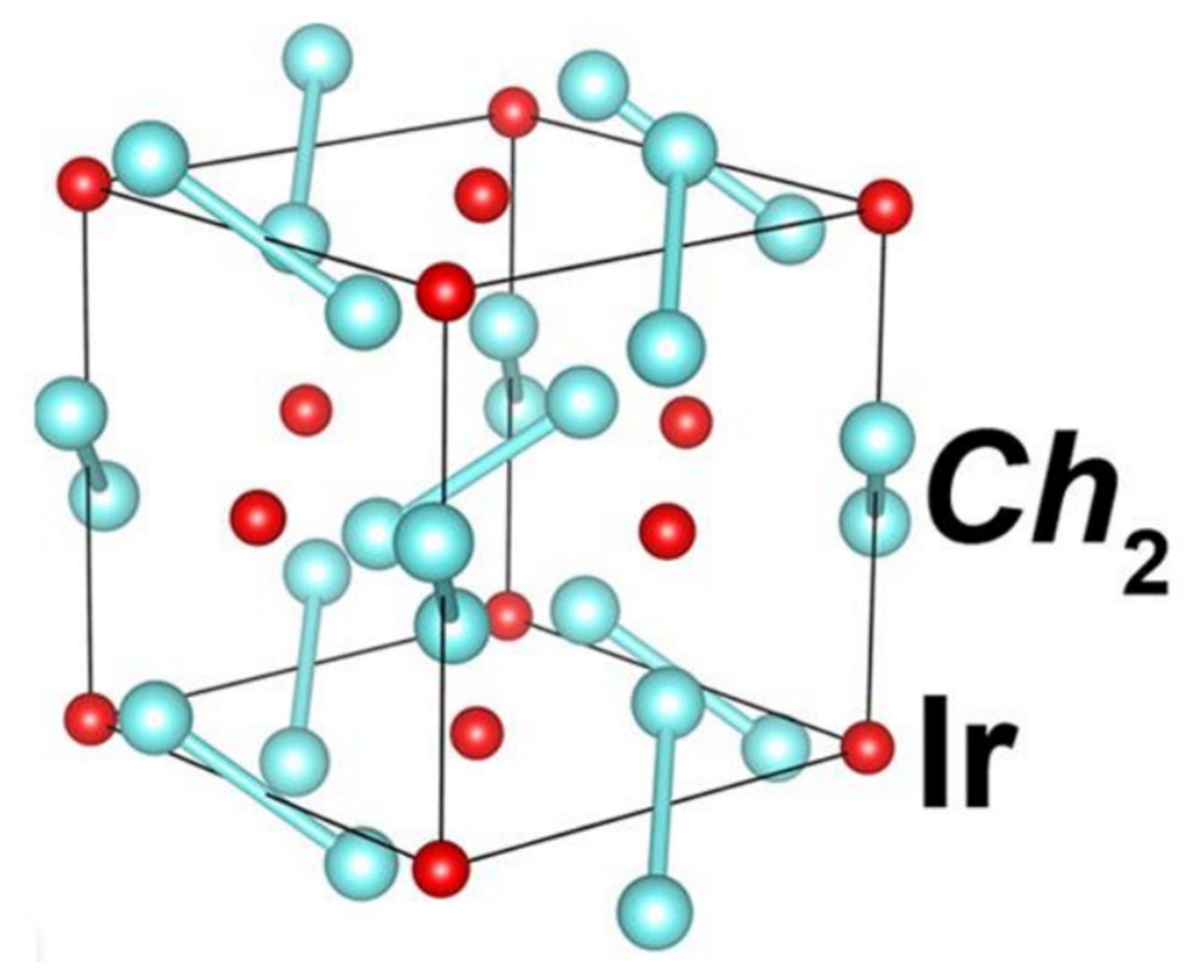
- Qi, Y.; Matsuishi, S.; Guo, J.; Mizoguchi, H.; Hosono, H. Superconductivity in Defective Pyrite-Type Iridium ChalcogenidesIrxCh2(Ch = Seand Te). Phys. Rev. Lett. 2012, 109, 217002. [Google Scholar] [CrossRef] [PubMed]
- Gor’Kov, L.P.; Rashba, E.I. Superconducting 2D System with Lifted Spin Degeneracy: Mixed Singlet-Triplet State. Phys. Rev. Lett. 2001, 87, 037004. [Google Scholar] [CrossRef]
- Frigeri, P.A.; Agterberg, D.F.; Sigrist, M. Spin susceptibility in superconductors without inversion symmetry. New J. Phys. 2004, 6, 115. [Google Scholar] [CrossRef]
- Frigeri, P.A.; Agterberg, D.F.; Koga, A.; Sigrist, M. Superconductivity without Inversion Symmetry: MnSi versusCePt3Si. Phys. Rev. Lett. 2004, 92, 097001. [Google Scholar] [CrossRef]
- Bauer, E.D.; Hilscher, G.; Michor, H.; Paul, C.; Scheidt, E.W.; Gribanov, A.V.; Seropegin, Y.; Noël, H.; Sigrist, M.; Rogl, P. Heavy Fermion Superconductivity and Magnetic Order in NoncentrosymmetricCePt3Si. Phys. Rev. Lett. 2004, 92, 027003. [Google Scholar] [CrossRef]
- Settai, R.; Sugitani, I.; Okuda, Y.; Thamizhavel, A.; Nakashima, M.; Ōnuki, Y.; Harima, H. Pressure-induced superconductivity in CeCoGe3 without inversion symmetry. J. Magn. Magn. Mater. 2007, 310, 844–846. [Google Scholar] [CrossRef]
- Kimura, N.; Ito, K.; Aoki, H.; Uji, S.; Terashima, T. Extremely High Upper Critical Magnetic Field of the Noncentrosymmetric Heavy Fermion SuperconductorCeRhSi3. Phys. Rev. Lett. 2007, 98, 197001. [Google Scholar] [CrossRef]
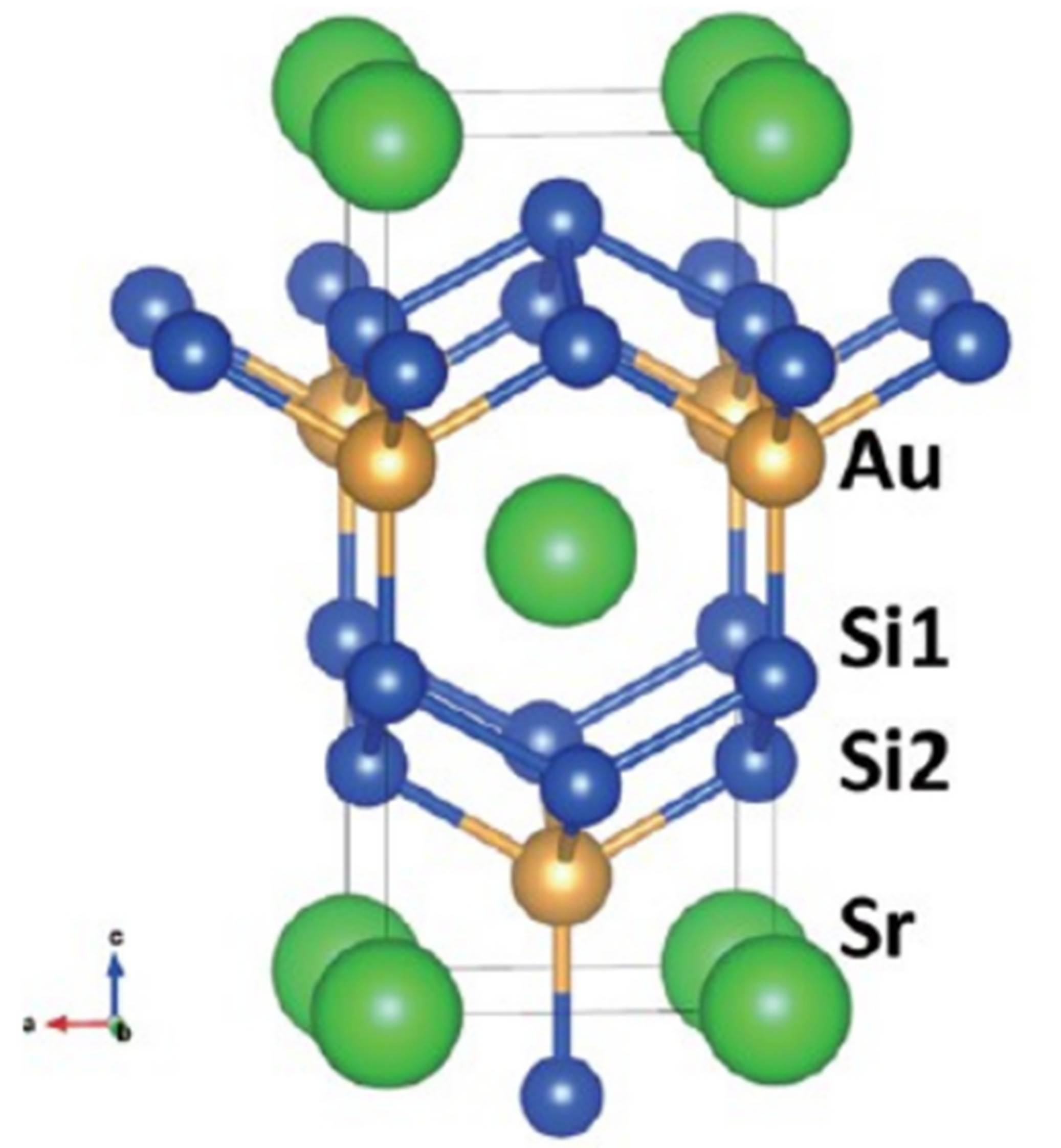
- Isobe, M.; Yoshida, H.; Kimoto, K.; Arai, M.; Takayama-Muromachi, E. SrAuSi3: A Noncentrosymmetric Superconductor. Cheminform 2014, 26, 2155–2165. [Google Scholar] [CrossRef]
- Pyon, S.; Kudo, K.; Matsumura, J.-I.; Ishii, H.; Matsuo, G.; Nohara, M.; Hojo, H.; Oka, K.; Azuma, M.; Garlea, V.O.; et al. Superconductivity in Noncentrosymmetric Iridium Silicide Li2IrSi3. J. Phys. Soc. Jpn. 2014, 83, 1–5. [Google Scholar] [CrossRef]
- McMillan, W.L. Transition Temperature of Strong-Coupled Superconductors. Phys. Rev. 1968, 167, 331–344. [Google Scholar] [CrossRef]
- Dynes, R. McMillan’s equation and the Tc of superconductors. Solid State Commun. 1972, 10, 615–618. [Google Scholar] [CrossRef]
- Zheng, X.; Zheng, J. Seeking high temperature superconductors in ambient from exemplary beryllium-based alloys. Solid State Commun. 2019, 306, 113769. [Google Scholar] [CrossRef]
- Ryu, G.; Kim, S.W.; Mizoguchi, H.; Matsuishi, S.; Hosono, H. Superconductivity in a PbFCl-type pnictide: NbSiAs. Eur. Lett. 2012, 99, 27002. [Google Scholar] [CrossRef]
- Mizoguchi, H.; Hosono, H. La2Sb, a layered superconductor with metal–metal bonds. Chem. Commun. 2011, 47, 3778–3780. [Google Scholar] [CrossRef] [PubMed][Green Version]
- Guo, J.; Yamaura, J.-I.; Lei, H.; Matsuishi, S.; Qi, Y.; Hosono, H. Superconductivity in Ban+2Ir4nGe12n+4(n = 1,2) with cage structure and softening of low-lying localized mode. Phys. Rev. B 2013, 88, 1–5. [Google Scholar] [CrossRef]
- Ryu, G.; Kim, S.W.; Matsuishi, S.; Kawaji, H.; Hosono, H. Superconductivity in Nb4MSi (M = Ni, Co, and Fe) with a quasi-two-dimensional Nb network. Phys. Rev. B 2011, 84, 1–6. [Google Scholar] [CrossRef]
- Li, Y.; Weng, Y.; Zhang, J.; Ding, J.; Zhu, Y.; Wang, Q.; Yang, Y.; Cheng, Y.; Zhang, Q.; Li, P.; et al. Observation of superconductivity in structure-selected Ti2O3 thin films. NPG Asia Mater. 2018, 10, 522–532. [Google Scholar] [CrossRef]
- Jeong, S.; Matsuishi, S.; Lee, K.; Toda, Y.; Kim, S.W.; Hosono, H. Superconductivity of Ca2InN with a layered structure embedding an anionic indium chain array. Arxiv Prepr. 2014, arXiv:1403.1348. [Google Scholar]
- Arpaia, R.; Golubev, D.; Baghdadi, R.; Ciancio, R.; Dražić, G.; Orgiani, P.; Montemurro, D.; Bauch, T.; Lombardi, F. Transport properties of ultrathin YBa2Cu3O7−δ nanowires: A route to single-photon detection. Phys. Rev. B 2017, 96, 064525. [Google Scholar] [CrossRef]
- Stepantsov, E.A.; Arpaia, R.; Lombardi, F. Growth of twin-free b-oriented YBa2Cu3O7 − x films. Crystallogr. Rep. 2015, 60, 393–396. [Google Scholar] [CrossRef]
- Stepantsov, E.A.; Lombardi, F.; Winkler, D. Growth of YBa2Cu3O7 films with [100] tilt of CuO planes to the surface on SrTiO3 crystals. Crystallogr. Rep. 2011, 56, 152–156. [Google Scholar] [CrossRef]
- Kislinskii, J.; Zhao, B.-R.; Wu, P.-J.; Peng, Z.-Q.; Chen, Y.-F.; Yang, T.; Chen, L.; Sun, J.-J.; Xu, B.; Wu, F.; et al. YBa2Cu3O7 Bicrystal Josephson Junctions and dc SQUIDs. Chin. Phys. Lett. 1996, 13, 390–393. [Google Scholar] [CrossRef]
- Carillo, F.; De Luca, G.M.; Montemurro, D.; Papari, G.P.; Salluzzo, M.; Stornaiuolo, D.; Tafuri, F.; Beltram, F. Coherent transport in extremely underdoped Nd1.2Ba1.8Cu3Oznanostructures. New J. Phys. 2012, 14, 1–10. [Google Scholar] [CrossRef]
- Chaix, L.; Ghiringhelli, G.; Peng, Y.; Hashimoto, M.; Moritz, B.; Kummer, K.; Brookes, N.; He, Y.; Chen, S.; Ishida, S.; et al. Dispersive charge density wave excitations in Bi2Sr2CaCu2O8+δ. Nat. Phys. 2017, 13, 952–956. [Google Scholar] [CrossRef]
- Shayesteh, P.; Tsyshevsky, R.; Urpelainen, S.; Rochet, F.; Bournel, F.; Gallet, J.-J.; Kuklja, M.M.; Schnadt, J.; Head, A.R. Experimental and theoretical gas phase electronic structure study of tetrakis(dimethylamino) complexes of Ti(IV) and Hf(IV). J. Electron Spectrosc. Relat. Phenom. 2019, 234, 80–85. [Google Scholar] [CrossRef]
- Burdastyh, M.V.; Postolova, S.V.; Proslier, T.; Ustavshikov, S.S.; Antonov, A.V.; Vinokur, V.M.; Mironov, A.Y. Superconducting phase transitions in disordered NbTiN films. Sci. Rep. 2020, 10, 1–7. [Google Scholar] [CrossRef]
- Janocha, E.; Pettenkofer, C. ALD of ZnO using diethylzinc as metal-precursor and oxygen as oxidizing agent. Appl. Surf. Sci. 2011, 257, 10031–10035. [Google Scholar] [CrossRef]
- Acharya, J.; Goul, R.; Romine, D.; Sakidja, R.; Wu, J. Effect of Al2O3 Seed-Layer on the Dielectric and Electrical Properties of Ultrathin MgO Films Fabricated Using In Situ Atomic Layer Deposition. ACS Appl. Mater. Interfaces 2019, 11, 30368–30375. [Google Scholar] [CrossRef] [PubMed]
- Weimer, A.W. Particle atomic layer deposition. J. Nanoparticle Res. 2019, 21, 1–42. [Google Scholar] [CrossRef] [PubMed]
- Van Toan, N.; Tuoi, T.T.K.; Inomata, N.; Toda, M.; Ono, T. Aluminum doped zinc oxide deposited by atomic layer deposition and its applications to micro/nano devices. Sci. Rep. 2021, 11, 1204. [Google Scholar] [CrossRef]
- Shibalov, M.V.; Mumlyakov, A.; Trofimov, I.; Timofeeva, E.; Sirotina, A.; Pershina, E.; Tagachenkov, A.; Anufriev, Y.; Zenova, E.; Porokhov, N.N.; et al. Multistep atomic layer deposition process for ultrathin superconducting NbN films with high critical current density on amorphous substrate. Supercond. Sci. Technol. 2021, 34, 085016. [Google Scholar] [CrossRef]
- Guerrero-Sanchez, J.; Chen, B.; Takeuchi, N.; Zaera, F. Role of oligomer structures in the surface chemistry of amidinate metal complexes used for atomic layer deposition of thin films. J. Mater. Res. 2019, 35, 720–731. [Google Scholar] [CrossRef]
- George, S.M. Atomic Layer Deposition: An Overview. Chem. Rev. 2009, 110, 111–131. [Google Scholar] [CrossRef]
- Tsai, F.-T.; Chao, C.-K.; Jhong, K.-J.; Chang, R.-C. Characterization of oxide barrier layers prepared by atomic layer deposition. Adv. Mech. Eng. 2017, 9, 1–7. [Google Scholar] [CrossRef]
- Oviroh, P.O.; Akbarzadeh, R.; Pan, D.; Coetzee, R.A.M.; Jen, T.-C. New development of atomic layer deposition: Processes, methods and applications. Sci. Technol. Adv. Mater. 2019, 20, 465–496. [Google Scholar] [CrossRef]
- Becker, M.; Sierka, M. Atomistic Simulations of Plasma-Enhanced Atomic Layer Deposition. Materials 2019, 12, 2605. [Google Scholar] [CrossRef]
- Seweryn, A.; Pielok, A.; Lawniczak-Jablonska, K.; Pietruszka, R.; Marcinkowska, K.; Sikora, M.; Witkowski, B.S.; Godlewski, M.; Marycz, K. Zirconium Oxide Thin Films Obtained by Atomic Layer Deposition Technology Abolish the Anti-Osteogenic Effect Resulting from miR-21 Inhibition in the Pre-Osteoblastic MC3T3 Cell Line. Int. J. Nanomed. 2020, 15, 1595–1610. [Google Scholar] [CrossRef]
- Tvarog, D.; Olejníček, J.; Kratochvíl, J.; Kšírová, P.; Poruba, A.; Hubička, Z.; Čada, M. Characterization of radical-enhanced atomic layer deposition process based on microwave surface wave generated plasma. J. Appl. Phys. 2021, 130, 013301. [Google Scholar] [CrossRef]
- Guo, Y.; Zou, Y.; Cheng, C.; Wang, L.; Made, R.I.; Goei, R.; Tan, K.W.; Li, S.; Tok, A.I.Y. Noble metal alloy thin films by atomic layer deposition and rapid Joule heating. Sci. Rep. 2022, 12, 1–9. [Google Scholar] [CrossRef] [PubMed]
- Sheng, J.; Lee, J.-H.; Choi, W.-H.; Hong, T.; Kim, M.; Park, J.-S. Review Article: Atomic layer deposition for oxide semiconductor thin film transistors: Advances in research and development. J. Vac. Sci. Technol. A: Vac. Surf. Film. 2018, 36, 060801. [Google Scholar] [CrossRef]
- Richey, N.E.; De Paula, C.; Bent, S.F. Understanding chemical and physical mechanisms in atomic layer deposition. J. Chem. Phys. 2020, 152, 040902. [Google Scholar] [CrossRef] [PubMed]
- Sowa, M.J.; Yemane, Y.; Zhang, J.; Palmstrom, J.C.; Ju, L.; Strandwitz, N.C.; Prinz, F.B.; Provine, J. Plasma-enhanced atomic layer deposition of superconducting niobium nitride. J. Vac. Sci. Technol. A Vac. Surf. Film. 2017, 35, 01B143. [Google Scholar] [CrossRef]
- Yemane, Y.T.; Sowa, M.J.; Zhang, J.; Ju, L.; Deguns, E.W.; Strandwitz, N.C.; Prinz, F.B.; Provine, J. Superconducting niobium titanium nitride thin films deposited by plasma-enhanced atomic layer deposition. Supercond. Sci. Technol. 2017, 30, 095010. [Google Scholar] [CrossRef]
- Zhang, K.; Balasubramanian, K.; Ozsdolay, B.; Mulligan, C.; Khare, S.; Zheng, W.; Gall, D. Growth and mechanical properties of epitaxial NbN(001) films on MgO(001). Surf. Coat. Technol. 2016, 288, 105–114. [Google Scholar] [CrossRef]
- Krishnan, R.; David, C.; Ajikumar, P.; Dash, S.; Tyagi, A.; Jayaram, V.; Raj, B. Reactive pulsed laser deposition and characterization of niobium nitride thin films. Surf. Coat. Technol. 2011, 206, 1196–1202. [Google Scholar] [CrossRef]
- Mamun, A.; Farha, A.; Er, A.; Ufuktepe, Y.; Gu, D.; Elsayed-Ali, H.; Elmustafa, A. Nanomechanical properties of NbN films prepared by pulsed laser deposition using nanoindendation. Appl. Surf. Sci. 2012, 258, 4308–4313. [Google Scholar] [CrossRef]
- Hinz, J.; Bauer, A.J.; Thiede, T.; Fischer, R.A.; Frey, L. Evaluation of NbN thin films grown by MOCVD and plasma-enhanced ALD for gate electrode application in high-k/SiO2gate stacks. Semicond. Sci. Technol. 2010, 25, 075009. [Google Scholar] [CrossRef]
- Van Hoornick, N.; De Witte, H.; Witters, T.; Zhao, C.; Conard, T.; Huotari, H.; Swerts, J.; Schram, T.; Maes, J.W.; De Gendt, S.; et al. Evaluation of Atomic Layer Deposited NbN and NbSiN as Metal Gate Materials. J. Electrochem. Soc. 2006, 153, G437–G442. [Google Scholar] [CrossRef]
- Thiede, T.B.; Parala, H.; Reuter, K.; Passing, G.; Kirchmeyer, S.; Hinz, J.; Lemberger, M.; Bauer, A.J.; Barreca, D.; Gasparotto, A.; et al. Deposition of Niobium Nitride Thin Films fromTert-Butylamido-Tris-(Diethylamido)-Niobium by a Modified Industrial MOCVD Reactor. Chem. Vap. Depos. 2009, 15, 334–341. [Google Scholar] [CrossRef]
- Gordon, R.G.; Liu, X.; Shi, Y. Highly conformal diffusion barriers of amorphous niobium nitride. Mat. Res. Soc. Symp. Proc. 1999, 564, 335–340. [Google Scholar] [CrossRef]
- Alén, P.; Ritala, M.; Arstila, K.; Keinonen, J.; Leskelä, M. The growth and diffusion barrier properties of atomic layer deposited NbNx thin films. Thin Solid Film. 2005, 491, 235–241. [Google Scholar] [CrossRef]
- Ziegler, M.; Fritzsch, L.; Day, J.; Linzen, S.; Anders, S.; Toussaint, J.; Meyer, H.-G. Superconducting niobium nitride thin films deposited by metal organic plasma-enhanced atomic layer deposition. Supercond. Sci. Technol. 2012, 26, 25008. [Google Scholar] [CrossRef]
- Chaudhuri, S.; Nevala, M.R.; Maasilta, I.J. Niobium nitride-based normal metal-insulator-superconductor tunnel junction microthermometer. Appl. Phys. Lett. 2013, 102, 132601. [Google Scholar] [CrossRef]
- Hiltunen, L.; Leskela, M.; Mäkelä, M.; Niinistö, L.; Nykänen, E.; Soininen, P. Nitrides of titanium, niobium, tantalum and molybdenum grown as thin films by the atomic layer epitaxy method. Thin Solid Film. 1988, 166, 149–154. [Google Scholar] [CrossRef]
- Klug, J.A.; Proslier, T.; Elam, J.W.; Cook, R.E.; Hiller, J.M.; Claus, H.; Becker, N.G.; Pellin, M.J. Atomic Layer Deposition of Amorphous Niobium Carbide-Based Thin Film Superconductors. J. Phys. Chem. C 2011, 115, 25063–25071. [Google Scholar] [CrossRef]
- Iosad, N.; Roddatis, V.; Polyakov, S.; Varlashkin, A.; Jackson, B.; Dmitriev, P.; Gao, J.; Klapwijk, T. Superconducting transition metal nitride films for THz SIS mixers. IEEE Trans. Appl. Supercond. 2001, 11, 3832–3835. [Google Scholar] [CrossRef]
- Krause, S.; Meledin, D.; Desmaris, V.; Pavolotsky, A.; Belitsky, V.; Rudziński, M.; Pippel, E. Epitaxial growth of ultra-thin NbN films on AlxGa1−xN buffer-layers. Supercond. Sci. Technol. 2014, 27, 65009. [Google Scholar] [CrossRef][Green Version]
- Shiino, T.; Shiba, S.; Sakai, N.; Yamakura, T.; Jiang, L.; Uzawa, Y.; Maezawa, H.; Yamamoto, S. Improvement of the critical temperature of superconducting NbTiN and NbN thin films using the AlN buffer layer. Supercond. Sci. Technol. 2010, 23, 045004. [Google Scholar] [CrossRef]
- Shoji, A.; Kiryu, S.; Kohjiro, S. Superconducting properties and normal-state resistivity of single-crystal NbN films prepared by a reactive rf-magnetron sputtering method. Appl. Phys. Lett. 1992, 60, 1624–1626. [Google Scholar] [CrossRef]
- Wang, Z.; Kawakami, A.; Uzawa, Y.; Komiyama, B. Superconducting properties and crystal structures of single-crystal niobium nitride thin films deposited at ambient substrate temperature. J. Appl. Phys. 1996, 79, 7837–7842. [Google Scholar] [CrossRef]
- Bhat, A.; Meng, X.; Wong, A.; Van Duzer, T. Superconducting NbN films grown using pulsed laser deposition for potential application in internally shunted Josephson junctions. Supercond. Sci. Technol. 1999, 12, 1030–1032. [Google Scholar] [CrossRef]
- Tamm, A.; Tarre, A.; Verchenko, V.; Seemen, H.; Stern, R. Atomic Layer Deposition of Superconducting CuO Thin Films on Three-Dimensional Substrates. Crystals 2020, 10, 650. [Google Scholar] [CrossRef]
- Wei, X.; Roy, P.; Yang, Z.; Zhang, D.; He, Z.; Lu, P.; Licata, O.; Wang, H.; Mazumder, B.; Patibandla, N.; et al. Ultrathin epitaxial NbN superconducting films with high upper critical field grown at low temperature. Mater. Res. Lett. 2021, 9, 336–342. [Google Scholar] [CrossRef]
- Gerbershagen, A.; Calzolaio, C.; Meer, D.; Sanfilippo, S.; Schippers, M. The advantages and challenges of superconducting magnets in particle therapy. Supercond. Sci. Technol. 2016, 29, 083001. [Google Scholar] [CrossRef]
- Jones, D.G.C. “Large Hadron Collider”. Encyclopedia Britannica, 22 December 2021. Available online: https://www.britannica.com/technology/Large-Hadron-Collider (accessed on 17 March 2022).
- Narlikar, A. The Oxford Handbook of Small Superconductors, 1st ed.; Oxford University Press: New York, NY, USA, 2017. [Google Scholar]
- Luiz, A. Overview of Possible Applications of High Tc Superconductors. In Applications of High-Tc Superconductivity; Federal University of Rio de Janeiro: Rio de Janeiro, Brazil, 2011; pp. 2–16. [Google Scholar]
- Norton, D.P. Science and technology of high-temperature superconducting films. Annu. Rev. Mater. Sci. 1998, 28, 299–347. [Google Scholar] [CrossRef]
- Sarker, M.M.; Flavell, W. Review of Applications of High-Temperature Superconductors. J. Supercond. 1998, 11, 209–213. [Google Scholar] [CrossRef]
- Parizh, M.; Lvovsky, Y.; Sumption, M. Conductors for commercial MRI magnets beyond NbTi: Requirements and challenges. Supercond. Sci. Technol. 2016, 30, 014007. [Google Scholar] [CrossRef]
- Lee, G.-J. Superconductivity Application in Power System. In Applications of High-Tc Superconductivity; Luiz, A., Ed.; Federal University of Rio de Janeiro: Rio de Janeiro, Brazil, 2011; pp. 46–66. [Google Scholar]
- Hawsey, R.A.; Morozumi, S. The Energy and Environmental Benefits of Superconducting Power Products. Mitig. Adapt. Strat. Glob. Chang. 2005, 10, 279–306. [Google Scholar] [CrossRef]
- Pereira, V.; Kunkolienkar, G.R. EMP (Electro-Magnetic Pulse) weapon technology along with EMP shielding & detection methodology. In Proceedings of the 2013 Fourth International Conference on Computing, Communications and Networking Technologies (ICCCNT), Tiruchengode, India, 4–6 July 2013; pp. 1–5. [Google Scholar] [CrossRef]
- Tou, H.; Tanaka, Y.J.; Sera, M.; Taguchi, Y.; Sasaki, T.; Iwasa, Y.; Zhu, L.; Yamanaka, S. Upper critical field in the electron-doped layered superconductorZrNCl0.7: Magnetoresistance studies. Phys. Rev. B 2005, 72, 020501. [Google Scholar] [CrossRef]
- Sugimoto, A.; Shohara, K.; Ekino, T.; Zheng, Z.; Yamanaka, S. Nanoscale electronic structure of the layered nitride superconductorsα-KxTiNCl andβ-HfNClyobserved by scanning tunneling microscopy and spectroscopy. Phys. Rev. B 2012, 85. [Google Scholar] [CrossRef]
- Grant, P.M. Challenges Confronting High Temperature Superconducting Materials: From Nanoscale Theories to Exascale Energy Applications. MRS Proc. 2014, 1684, 1–9. [Google Scholar] [CrossRef]


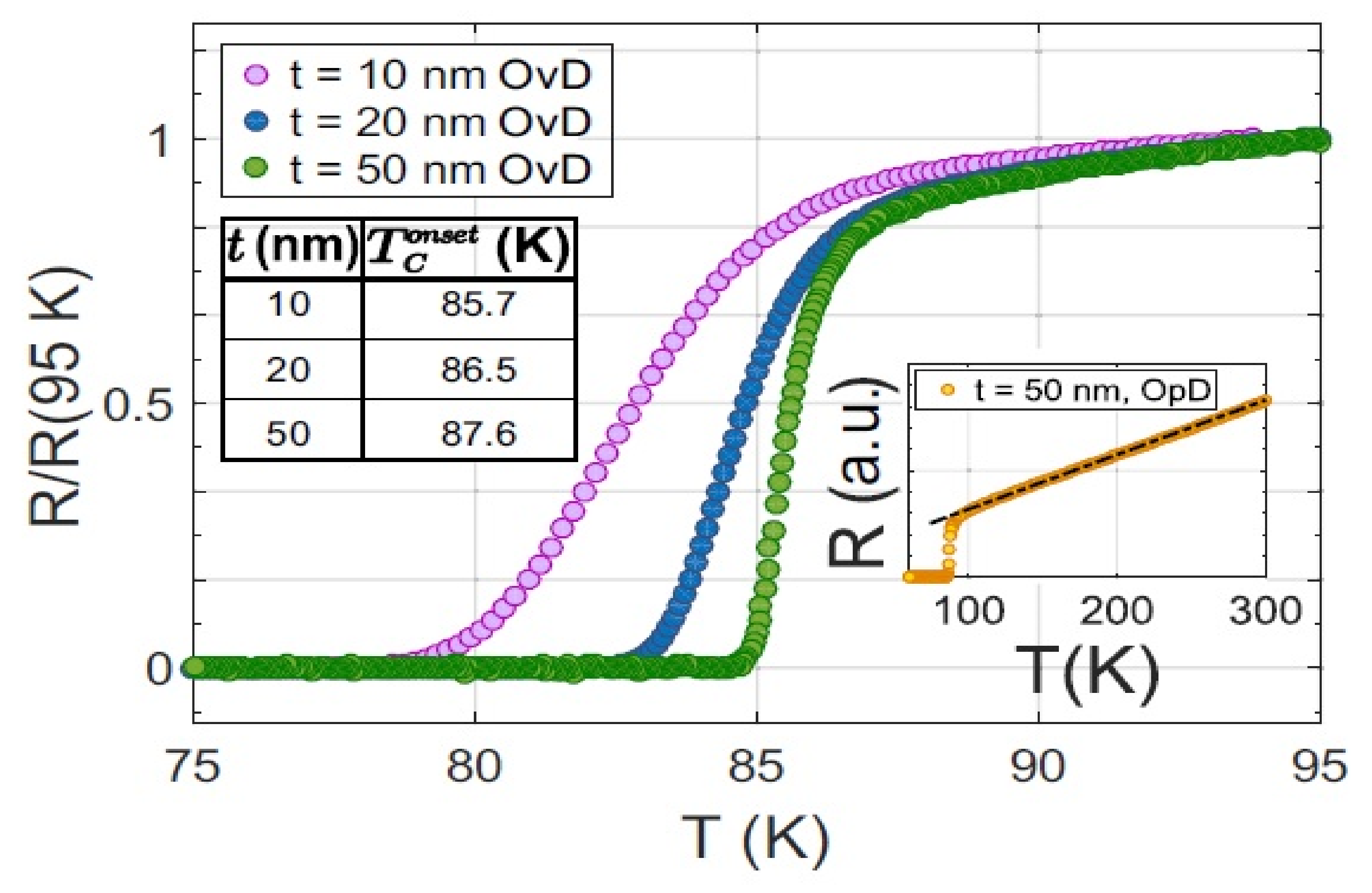
| Materials | Substrate | Method | Transition Temp (K) | References |
|---|---|---|---|---|
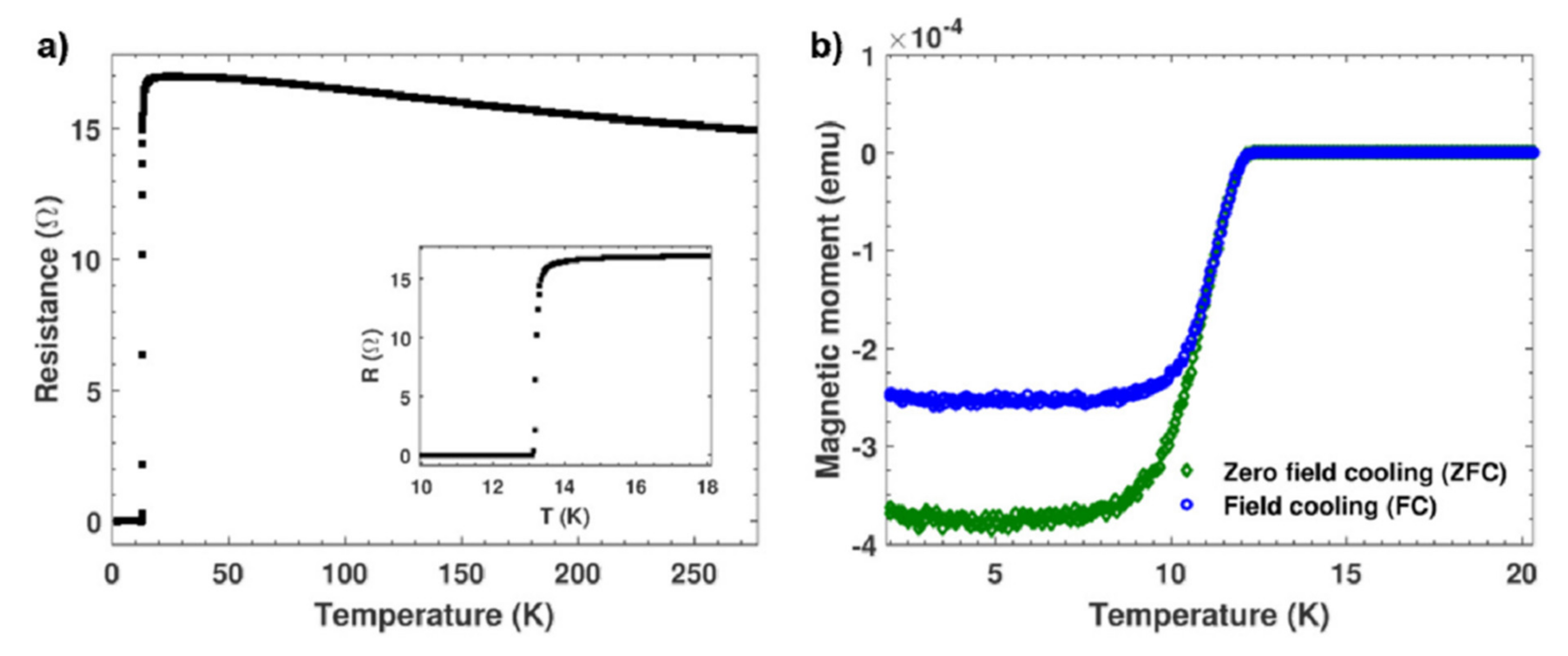
| FeSe | r-cut Al2O3 | MBE | Tc(onset) = 13 K | [70] |
| CaF2 | PLD | Tc(onset)= 12.4 K, Tc(end) = 11.9 K | [81] | |
| mono-layer FeSe | SrTiO3 | MBE | Tc = 42 K | [82] |
| SrTiO3 | Tc = 65 ± 5 K | [83] | ||
| Nb-doped SrTiO3 | Tc = 109 K | [84] | ||
| FeSe1−xTex x = 0.0~1.0 | MgO | PLD | Tc(onset)~14 K, Tc(end) ~ 12 K at x = 0.5 | [74] |
| FeSe0.5Te0.5 | SrTiO3 | PLD | Tc = 17 K | [85] |
| FeSe0.5Te0.5 | LaAlO3 | PLD | Tc = 21 K | [85] |
| FeSe0.5Te0.5 | CaF2 | PLD | Tc(onset) = 16.3 K, Tc(end) = 15.3 K | [63] |
| FeSe0.8Te0.2 | PLD | Tc = 23 K | [86] | |
| FeSe0.72Te0.18 | PLD | Tc(onset) = 22 K, Tc(end) = 20.5 K | [87] | |
| FeSe0.5Te0.5 | SrF2 | PLD | Tc = 15.7 K | [88] |
| FeSe0.5Te0.5 | BaF2 | PLD | Tc = 12.8 K | |
| FeSe0.5Te0.5 | Fe-buffered MgO | PLD | Tc = 17.7 K | [21,89] |
| FeSe0.5Te0.5 | CeO2-buffered YSZ, RABiTS | PLD | Tc(onset) = 20 K, Tc(end) = 18 K | [90] |
| FeSe0.5Te0.5 | CeO2-buffered SrTiO3 | PLD | Tc(onset) = 18.5 K, Tc(end) = 18 K | [91] |
| FeSe0.5Te0.5 | FeSe1−xTex-buffered MgO | PLD | Tc(onset) ≥ 17 K | [92] |
Publisher’s Note: MDPI stays neutral with regard to jurisdictional claims in published maps and institutional affiliations. |
© 2022 by the authors. Licensee MDPI, Basel, Switzerland. This article is an open access article distributed under the terms and conditions of the Creative Commons Attribution (CC BY) license (https://creativecommons.org/licenses/by/4.0/).
Share and Cite
Sibanda, D.; Oyinbo, S.T.; Jen, T.-C.; Ibitoye, A.I. A Mini Review on Thin Film Superconductors. Processes 2022, 10, 1184. https://doi.org/10.3390/pr10061184
Sibanda D, Oyinbo ST, Jen T-C, Ibitoye AI. A Mini Review on Thin Film Superconductors. Processes. 2022; 10(6):1184. https://doi.org/10.3390/pr10061184
Chicago/Turabian StyleSibanda, David, Sunday Temitope Oyinbo, Tien-Chien Jen, and Ayotunde Idris Ibitoye. 2022. "A Mini Review on Thin Film Superconductors" Processes 10, no. 6: 1184. https://doi.org/10.3390/pr10061184
APA StyleSibanda, D., Oyinbo, S. T., Jen, T.-C., & Ibitoye, A. I. (2022). A Mini Review on Thin Film Superconductors. Processes, 10(6), 1184. https://doi.org/10.3390/pr10061184