Abstract
Silica (SiO2, silicon dioxide—a dielectric layer commonly used in electronic devices) is widely used in many types of sensors, such as gas, molecular, and biogenic polyamines. To form silica films, core shell or an encapsulated layer, silane has been used as a precursor in recent decades. However, there are many hazards caused by using silane, such as its being extremely flammable, the explosive air, and skin and eye pain. To avoid these hazards, it is necessary to spend many resources on industrial safety design. Thus, the silica synthesized without silane gas which can be determined as a silane-free procedure presents a clean and safe solution to manufactures. In this report, we used the radio frequency (rf = 13.56 MHz) plasma-enhanced chemical vapor deposition technique (PECVD) to form a silica layer at room temperature. The silica layer is formed in hydrogen-based plasma at room temperature and silane gas is not used in this process. The substrate temperature dominates the silica formation, but the distance between the substrate and electrode (DSTE) and the methane additive can enhance the formation of a silica layer on the Si wafer. This silane-free procedure, at room temperature, is not only safer and friendlier to the environment but is also useful in the fabrication of many types of sensors.
1. Introduction
The most popular application for silica is the dielectric layer [1] and spacer [2] in the processing of integral circuits. Furthermore, there have been some novel applications in biotechnology [3,4,5], photoelectric technique [6], organic photoresists [7,8,9,10] and sensors [11,12,13,14]. Silica is especially widely used in many types of sensors, such as gas, molecular and biogenic polyamines [7,8,9,10,11,12,13,14]. For example, the silica functionalization process is used to immobilize a variety of biomolecules, including glucose oxidase, horseradish peroxide, metallothionein, and DNA molecules [11]. A solid-state electrochemiluminescence sensor based on Ru(bpy)32+-encapsulated silica nanoparticles, covalently immobilized on a screen-printed carbon electrode, has been developed and characterized [14]. Among those novel applications, the processing temperature plays a crucial role in the final production yield for applications, not only in the processing of integral circuits, but also in biotechnology. The method used to process silica is the direct exposure of oxygen to a Si wafer with a processing temperature from 900 to 1200 degrees Celsius (°C) [15]. In the 2000s, silane was announced as the main material used to fulfill the low-temperature silica deposition, with the technology of plasma-enhanced chemical vapor deposition (PECVD) [16,17]. In addition, to achieve fewer defects and higher uniformity, the processing temperature is pushed to a limit of from around 50 to 200 °C for silica deposition by the low-temperature or plasma-enhanced atomic layer deposition (ALD) technique [18,19,20,21]. However, silane has many dangers due to its flammable, explosive properties. Therefore, the environment is confirmed to be clean and safe when silane is not used in the fabricating procedure. In this report, we offer a silane-free procedure for depositing silica on a 12” silicon wafer at room temperature in a hydrogen-based plasma by PECVD technique. The substrate temperature dominates the silica formation, but the DSTE and methane additive can both enhance the formation of silica layer on the Si wafer. This silane-free procedure at room temperature is not only safer and friendlier to the environment, but also useful in the fabrication of many types of sensors. We may produce a chemo-sensor by utilizing silica, and the schematic plot of the sensor head is shown in Figure 1. First, the silica films are deposited on top of the Si substrate as a gate between the source and drain, which is produced by an ion plant. The shape and alignment of the gate, source and drain are simply, schematically shown in Figure 1. On top of the silica gate, a blocking sheet is deposited to absorb the specific kind of aptamer. Therefore, the target material will be successful in sensing. To summarize, the hydrogen-based plasma by PECVD technique can be perfectly controlled and is able to synthesize the silica layer on the Si substrate at room temperature. Thus, the silica layer can be widely used in many types of sensors, such as gas, molecular and biogenic polyamines.
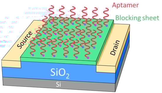
Figure 1.
The schematic plot for sensors in universal construction contains source and drain electrode, gate (SiO2 layer), base (Si substrate), blocking sheet and aptamers.
2. Materials and Methods
A 12-inch Si (100) wafer is used as the substrate of silica deposition. The contaminations and native silica on substrate surface are cleaned by the Radio Corporation of America (RCA) cleaning process. After the cleaning procedure, the wafer is loaded to the chamber of ULVAC-PECVD with 13.56 MHz radio frequency signal. The electrode is suitable for 12” wafer production with a 300 × 400 mm rectangle showerhead, which offers plenty of gas inlets to deliver the process gas to the substrate surface, with a methane, oxygen and hydrogen gas of 99.999% purity. The mixture for CH4 and oxygen of 500 ppm is simultaneously delivered in the processing chamber with hydrogen with a flow rate of 37:100 sccm. At this moment, the concentration of CH4 can be determined as 27%. The deposition experiments of silica are carried out under the reaction pressure of 133 Pa and a distance between substrate and electrode (DSTE) of 40 mm, combined with an rf-power of 250 W. This processing recipe design was mainly chosen to use the hydrogen plasma as a background in order to form silica. The methane molecular is the most similar material in terms of atom composition, and is used to replace silane in the plasma conditions for PECVD. Although there are no Si atoms in the methane molecular, the methane molecular still supplies considerable energy to the oxygen and Si wafer to synthesize the silica layer at room temperature. The extremely low flux of oxygen may limit the synthesizing rate for silica; the lower synthesizing rate always can obtain a much more uniform layer and fewer defects [22,23]. The large flux in hydrogen is used to etch carbon atoms and silica clusters [24,25,26]. In this report, we especially use the hydrogen to etch and deposit silica at the same time, which may enhance the uniformity and reduce the defects. This idea is inspired by the self-ion sputtering technique [27,28,29]. Surface morphologies, cross-sections and energy-dispersive X-ray analysis of the deposited films are examined with JEOL scanning electron microscopy (SEM). Atomic force microscopy (AFM) is also employed to investigate the surface morphology of silica films. The thickness of the deposited films can be calculated by the fitting data from ellipsometry. The incident beam of ellipsometry measurement is set up from 45 to 60 degrees (5 degrees/measurement). The result is well fitted for all data at the same model in a series measurement. The light source, Quartz Tungsten Halogen (QTH) lamp is within a reliable scanning range from visible to near-infrared (NIR), which is suitable for measuring the silica layer. The refraction index n and dielectric constant k can also be calculated by the analysis of ellipsometry measurement. In Figure 2a–c, the ellipsometry results for native oxide, deposition time of 20 and 40 min, are shown, respectively. The scanning angle for Figure 2a–c is between 45 and 60 degrees. In order to get the thickness of the silica films for Figure 2a–c, the ellipsometry results should be fitted by the commercial software. Because the light source for the ellipsometry measurements is sensitive for the wavelength between 350 and 1000 nm, the fitting range is chosen to be between 350 and 1000 nm. After the analysis, the ellipsometry results in Figure 2a–c are all well-fitted, indicating that the silica thin films deposited by this recipe are perfectly fitted to be a uniform silica layer on the Si wafer. This is a common and standard analysis using ellipsometry results to confirm the thickness of silica thin films [30,31].
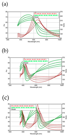
Figure 2.
The ellipsometry results for (a) native oxide and silicon dioxide with deposition times of (b) 20 and (c) 40 min are measured and fitted by the EASE program from J. A. Woollam Co., Inc., Lincoln, NE, USA.
3. Results and Discussion
3.1. Optical and SEM Measurements for the Silica Layer
The systematical data are shown in Figure 3a. The stable linear increase in the thickness of silica can be observed as the deposition time increases, indicating that the deposition rate is 3.5 nm/min. Furthermore, the inset in Figure 3a simultaneously shows the high uniformity of thin films and the thickness of 210 nm, which coincides with the results from ellipsometry. The systematical research on different substrate temperatures, CH4 concentration and DSTE are carried out under the standard of this recipe in order to find out the dominant condition and mechanism of the silica deposition. In Figure 3b, the thickness of silica thin film decreases from 210 to 4 nm as the substrate temperature increases from room temperature to 150 °C. The thickness of silica thin film remains from 3 to 4 nm, which coincides with the native oxide of the silicon wafer. The inset in Figure 3b is the energy-dispersive X-ray spectroscopy (EDS) and Raman spectrum of the SiO2 layer, indicating that it is a pure silica film without carbon atoms, with the feeding of methane gas. This result implies that a substrate is over 150 °C is not beneficial for silica deposition. This phenomenon can be attributed to the thermal disturbance and hydrogen plasma etching between 150 and 300 °C. The thermal disturbance is not beneficial for the oxide adsorption and chemical combination on the substrate surface, which has been reported in the literature as different material interfaces [32,33,34]. In addition, the hydrogen plasma can etch the silica layer and carbon atoms with a higher temperature [24,25,26]. From the results mentioned above, 150 °C is the transition point for the deposition of silica under the influence of substrate temperature. Therefore, the comparison of the experimental results with a substrate temperature of 100 and 200 °C is focused on in the following research.
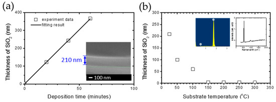
Figure 3.
(a) The thickness of SiO2 from ellipsometry results and fitting by a linear behavior in deposition time. The inset plot is the cross-section SEM image for a deposition time of 60 min. (b) The relationship between the thickness of the SiO2 layer and substrate temperature from room temperature to 300 °C with 27% CH4, 500 ppm O2, DSTE = 40 mm.
3.2. Methane Additive Enhanced the Silica Layer
The effect of DSTE on silica deposition is shown in Figure 4a. At a substrate temperature of 100 °C, as DSTE increases from 10 to 40 mm, and the thickness of silica thin film reduces from 250 to 50 nm. Most importantly, a linear relationship can be observed when DSTE is between 10 and 30 mm. This result indicates that it can be discussed by simplifying the model for the parallel plate capacitor [35]. The DSTE can be considered as the capacitor distance, and the capacity (C) can be expressed by Equation (1):
where A is the area of the capacitor plates and ε is the permittivity of dielectric. When the plasma is stable, A and ε are assumed to be constants. Therefore, the capacity is proportional to 1/DSTE. Compared with the experimental results, the deposition rate, being proportional to capacity and 1/DSTE, can be concluded. Therefore, the capacity is higher with a smaller DSTE, resulting in its owning sufficient energy to help the deposition of silica thin film. However, when DSTE is longer than 30 mm, it deviates from the prediction of the parallel plate capacitor model, which can be attributed to the interval being too big to let the gas-flow fill the whole capacitor. The results in the thickness of silica deposition being lower than predicted. Nevertheless, when the substrate temperature is 200 °C, the silica cannot successfully be deposited on a silicon wafer by tuning DSTE.
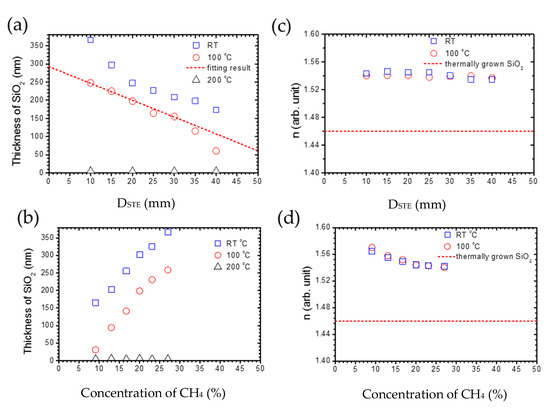
Figure 4.
The relationship between the thickness of the SiO2 layer and (a) DSTE from 10 to 40 mm with 27 % CH4, 500 ppm O2 at 100 and 200 °C, and (b) the concentration of CH4 from 9 to 27% with 500 ppm O2, DSTE = 10 mm at room temperature, 100 and 200 °C. The deposition time is an hour. (c,d) are the respective refraction indexes n for (a,b).
On the other hand, the thickness of the silica thin film versus concentration of CH4 is shown in Figure 4b with oxygen levels at 500 ppm and DSTE at 10 mm. At a substrate temperature of 100 °C, the thickness of silica increases significantly when the concentration of CH4 increases. The reason for this is that the increased concentration of CH4 can significantly enhance the plasma density [36], resulting in the enhancement of chemical reactions between Si and O atoms. However, when the substrate temperature is 200 °C, the silica cannot be successfully deposited on a silicon wafer by a tuning concentration of CH4. Furthermore, to discuss the quality of silica films, the refraction index n is necessary. The refraction index n for the light source with a wavelength of 632.8 nm can be calculated from the analysis of ellipsometry results. As the silica films are successfully deposited at the deposition temperature of room temperature and 100 °C, we will discuss only the n for series at a deposition temperature of room temperature and 100 °C. The effect of DSTE on the n of silica films is shown in Figure 4c. When the DSTE increases from 10 to 40 nm, n for silica films deposited at room temperature and 100 °C is almost consistent at 1.54. The extinction coefficient is almost zero. This implies that the quality of silica films is not influenced by DSTE. On the other hand, the refraction index with a different concentration of CH4 is shown in Figure 4d. With the increasing concentration of CH4, n slightly decreases from 1.57 to 1.54 for silica films deposited at room temperature and 100 °C. The extinction coefficient is almost zero. The dash line is the refraction index for the thermally grown silica film, whose value is 1.46 [37]. The decrease in n can be attributed to the increase in the pinholes, because n for pure silica films is 1.6. In summary, the substrate temperature dominates the silica formation, but the DSTE and methane additive can both enhance the formation of a silica layer on the Si wafer.
3.3. Uniformity Measurements for the Silica Layer
Therefore, that recipe is adopted to the uniformity research of large-area deposition on an industrial-size 12” Si wafer, which is shown in Figure 5. In Figure 5a, the thickness of silica remains at 360 and 250 nm for the deposition temperature of RT and 100 °C, respectively, when the distance to the center of the silicon wafer increases from 0 to 6”. After calculating the uniformity of the silica thin film, which can be defined by the ratio between the thickness of silica thin film at x” and the center of silicon wafer, we can see that the uniformity remains at 1.0, which is shown in Figure 5b. In Figure 5c, the refraction index of silica remains near 1.54 for a deposition temperature of room temperature and 100 °C, but the refraction index of silica deposited at room temperature is a little bigger than the silica deposited at 100 °C. The extinction coefficient is almost zero. In Figure 5d, the dielectric constants of silica are consistent at 2.39 and 2.37 for deposition temperatures of room temperature and 100 °C, respectively. The dashed line is the refraction index for thermally grown silica film, whose value is 2.2 [38].
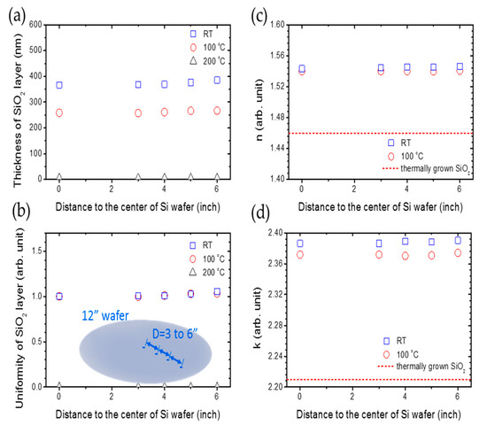
Figure 5.
The relationship between (a) the thickness of the SiO2 layer, (b) the uniformity of the SiO2 layer, (c) refraction index n, (d) dielectric constant k and the distance to the center of the Si wafer with a concentration of 27% CH4, 500 ppm O2, DSTE = 10 mm at room temperature, 100 and 200 °C. The deposition time is an hour.
The AFM images for silica deposition at room temperature and 100 °C at the center of the Si wafer are shown in Figure 6a,b respectively. The roughness for silica films deposited at room temperature is steady at 0.32 nm for any position at the 12” Si wafer, while the roughness for silica films deposited at 100 °C is steady at 1.02 nm. The red circle marks in Figure 6a,b represent the locations of pinholes in the silica films, and the average diameter and depth of pinholes are 100 and 2 nm, respectively. This implies that the formations of silica thin film in this recipe is not influenced by the distance to the center of the Si wafer when the wafer is smaller than 12”. Therefore, a large-area silica deposition can be fulfilled from this recipe.
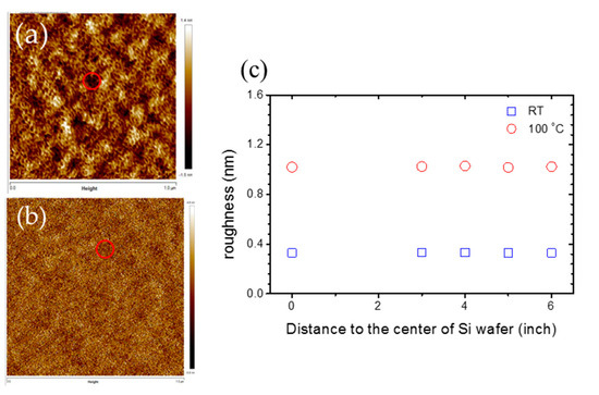
Figure 6.
The atomic force microscopy (AFM) images for the SiO2 layer deposited at (a) room temperature and (b) 100 °C at the center of the Si wafer; (c) is the roughness of k and the distance to the center of the Si wafer with a concentration of 27% CH4, 500 ppm O2, DSTE = 10 mm. The deposition time is an hour.
4. Conclusions
We successfully use the rf-PECVD to form a silica layer on the 12” Si wafer at room temperature in a hydrogen-based plasma. The substrate temperature dominates the silica formation, but the DSTE and methane additive can both enhance the formation of the silica layer on the Si wafer. The EDS and Raman spectrum of the SiO2 layer indicate that this is a pure silica film, without carbon atoms and with the feeding of methane gas. The refraction index and dielectric constant analysis imply that the silica film from this recipe is better than the thermally grown silica. Furthermore, this silane-free procedure at room temperature is not only safer and friendlier to the environment but is also useful in the fabrication of many types of sensors, such as gas, molecular and biogenic polyamines.
Author Contributions
Conceptualization, C.-H.-T.C. and C.-R.L.; data curation, P.-C.J., Y.-T.C. and C.-W.C.; formal analysis, P.-C.J., Y.-T.C. and C.-W.C.; investigation, P.-C.J., Y.-T.C. and C.-W.C.; methodology, C.-H.-T.C.; supervision, C.-H.-T.C. and C.-R.L.; validation, P.-C.J. and Y.-T.C.; writing—original draft, P.-C.J. and Y.-T.C.; writing—review and editing, C.-H.-T.C. All authors have read and agreed to the published version of the manuscript.
Funding
This research was funded by Contract Nos. MOST 108-2622-E-159-003-CC2, MOST 109-2112-M-159-001-MY2, and MOST 109-2221-E-159-001.
Institutional Review Board Statement
Not applicable.
Informed Consent Statement
Not applicable.
Data Availability Statement
Data sharing not applicable.
Acknowledgments
The authors wish to acknowledge support from Ministry of Science and Technology of Republic of China under Contract Nos. MOST 108-2622-E-159-003-CC2, MOST 109-2112-M-159-001-MY2, and MOST 109-2221-E-159-001. We also would like to acknowledge Ulvac Taiwan Inc. for providing their Cluster-type PE-CVD System: CME-400.
Conflicts of Interest
The authors declare no conflict of interest.
References
- Wu, X.; Xing, Y.; Zeng, K.; Huber, K.; Zhao, J.X. Study of Fluorescence Quenching Ability of Graphene Oxide with a Layer of Rigid and Tunable Silica Spacer. Langmuir 2017, 34, 603–611. [Google Scholar] [CrossRef]
- Liu, L.; Lv, F.; Li, P.; Ding, L.; Tong, W.; Chu, P.K.; Zhang, Y. Preparation of ultra-low dielectric constant silica/polyimide nanofiber membranes by electrospinning. Compos. Part A: Appl. Sci. Manuf. 2016, 84, 292–298. [Google Scholar] [CrossRef]
- Shang, Y.; Li, N.; Liu, S.; Wang, L.; Wang, Z.; Zhang, Z.; Ding, B. Site-Specific Synthesis of Silica Nanostructures on DNA Origami Templates. Adv. Mater. 2020, 32, e2000294. [Google Scholar] [CrossRef]
- Nguyen, T.L.; Choi, Y.; Kim, J. Mesoporous Silica as a Versatile Platform for Cancer Immunotherapy. Adv. Mater. 2019, 31, 1803953-1–1803953-7. [Google Scholar] [CrossRef] [PubMed]
- Martino, N.; Kwok, S.J.J.; Liapis, A.C.; Forward, S.; Jang, H.; Kim, H.-M.; Wu, S.J.; Wu, J.; Dannenberg, P.H.; Jang, S.-J.; et al. Wavelength-encoded laser particles for massively multiplexed cell tagging. Nat. Photonics. 2019, 13, 720–727. [Google Scholar] [CrossRef] [PubMed]
- Ilic, O.; Atwater, H.A. Self-stabilizing photonic levitation and propulsion of nanostructured macroscopic objects. Nat. Photonics. 2019, 13, 289–295. [Google Scholar] [CrossRef]
- Pasini, D.; Takeuchi, D. Cyclopolymerizations: Synthetic Tools for the Precision Synthesis of Macromolecular Architectures. Chem. Rev. 2018, 118, 8983–9057. [Google Scholar] [CrossRef]
- Fang, G.; Cao, H.; Cao, L.; Duan, X. Femtosecond Laser Direct Writing of 3D Silica-like Microstructure from Hybrid Epoxy Cyclohexyl POSS. Adv. Mater. Technol. 2017, 3, 1700271. [Google Scholar] [CrossRef]
- Klopp, J.M.; Pasini, D.; Byers, J.D.; Willson, C.G.; Fréchet, J.M.J. Microlithographic Assessment of a Novel Family of Transparent and Etch-Resistant Chemically Amplified 193-nm Resists Based on Cyclopolymers. Chem. Mater. 2001, 13, 4147–4153. [Google Scholar] [CrossRef]
- Lee, C.-K.; Don, T.-M.; Lai, W.-C.; Chen, C.-C.; Lin, D.-J.; Cheng, L.-P. Preparation and properties of nano-silica modified negative acrylate photoresist. Thin Solid Films 2008, 516, 8399–8407. [Google Scholar] [CrossRef]
- Sciuto, E.L.; Bongiorno, C.; Scandurra, A.; Petralia, S.; Cosentino, T.; Conoci, S.; Sinatra, F.; Libertino, S. Functionalization of Bulk SiO2 Surface with Biomolecules for Sensing Applications: Structural and Functional Characterizations. Chemosensors 2018, 6, 59. [Google Scholar] [CrossRef]
- Zahmouli, N.; Marini, S.; Guediri, M.; Ben Mansour, N.; Hjiri, M.; El Mir, L.; Espro, C.; Neri, G.; Leonardi, S.G. Nanostructured Nickel on Porous Carbon-Silica Matrix as an Efficient Electrocatalytic Material for a Non-Enzymatic Glucose Sensor. Chemosensors 2018, 6, 54. [Google Scholar] [CrossRef]
- Li, Z. Nanoporous Silica-Dye Microspheres for Enhanced Colorimetric Detection of Cyclohexanone. Chemosensors 2018, 6, 34. [Google Scholar] [CrossRef]
- Spehar-Délèze, A.-M.; Almadaghi, S.; O’Sullivan, C.K. Development of Solid-State Electrochemiluminescence(ECL) Sensor Based on Ru(bpy)32+-Encapsulated Silica Nanoparticles for the Detection of Biogenic Polyamines. Chemosensors 2015, 3, 178–189. [Google Scholar] [CrossRef]
- Osburn, C.M.; Ormond, D.W. Dielectric Breakdown in Silica Films on Silicon: II Influence of Processing and Materials. J. Electrochem. Soc. 1972, 119, 597–603. [Google Scholar] [CrossRef]
- Lee, J.W.; Mackenzie, K.D.; Johnson, D.; Sasserath, J.N.; Pearton, S.J.; Ren, F. Low Temperature Silicon Nitride and Silica Film Processing by Inductively Coupled Plasma Chemical Vapor Deposition. J. Electrochem. Soc. 2000, 147, 1481–1486. [Google Scholar] [CrossRef]
- Rodr´iguez, J.A.; Llobera, A.; Domínguez, C. Evolution of the mechanical stress on PECVD silicon oxide films under thermal processing. J. Mater. Sci. Lett. 2000, 19, 1399–1401. [Google Scholar] [CrossRef]
- Sheng, J. Performance and Stability Enhancement of In−Sn−Zn−O TFTs Using SiO2 Gate Dielectrics Grown by Low Temperature Atomic Layer Deposition. ACS Appl. Mater. Interfaces 2017, 9, 42928–42934. [Google Scholar] [CrossRef]
- Kim, D.H.; Lee, H.J.; Jeong, H.; Shong, B.; Kim, W.-H.; Park, T.J. Thermal Atomic Layer Deposition of Device-Quality SiO2 Thin Films under 100 °C Using an Aminodisilane Precursor. Chem. Mater. 2019, 31, 5502–5508. [Google Scholar] [CrossRef]
- Hiller, D.; Zierold, R.; Bachmann, J.; Alexe, M.; Yang, Y.; Gerlach, J.W.; Stesmans, A.; Jivanescu, M.; Müller, U.; Vogt, J.B.; et al. Low temperature silicon dioxide by thermal atomic layer deposition: Investigation of material properties. J. Appl. Phys. 2010, 107, 064314. [Google Scholar] [CrossRef]
- Lee, Y.-S.; Choi, D.-W.; Shong, B.; Oh, S.; Park, J.-S. Low temperature atomic layer deposition of SiO2 thin films using diisopropylaminosilane and ozone. Ceram. Int. 2017, 43, 2095–2099. [Google Scholar] [CrossRef]
- Johnson, R.W.; Hultqvist, A.; Bent, S.F. A brief review of atomic layer deposition: From fundamentals to applications. Mater. Today 2014, 17, 236–246. [Google Scholar] [CrossRef]
- Herman, M.A. Molecular Beam Epitaxy: Fundamentals and Current Status; Springer: Berlin Heidelberg, Germany, 2012. [Google Scholar]
- Behr, M.J.; Gaulding, E.A.; Mkhoyan, K.A.; Aydil, E.S. Hydrogen etching and cutting of multiwall carbon nanotubes. J. Vac. Sci. Technol. B 2010, 28, 1187–1194. [Google Scholar] [CrossRef][Green Version]
- Chang, R.P.H. Hydrogen etching of Semconductors and Oxides. U.S. Patent 4,361,461, 30 November 1982. [Google Scholar]
- Zaitsu, M.; Kobayashi, N.; Kobayashi, A.; Hori, M.; Tsutsumi, T. Method of Atomic Layer Etching Using Hydrogen Plasma. U.S. Patent No US 10,504,742 B2, 10 October 2019. [Google Scholar]
- Sakamoto, Y.; Kamada, K.; Hamaguchi, J.; Sano, A.; Numata, Y.; Kodaira, S.; Suu, K. Improved Step Coverage of Cu Seed Layers by Magnetic-Field-Assisted Ionized Sputtering. Jpn. J. Appl. Phys. 2011, 50, 05EA03. [Google Scholar] [CrossRef]
- Ding, P.; Xu, Z.; Mosely, R.; Rengarajan, S.; Maity, N.; Carl, D.; Forster, J. Self-Ionized and Inductively Coupled Plasma for Sputtering and Resputtering. U.S. Patent No US 8,696,875 B2, 15 April 2014. [Google Scholar]
- Ding, P.; Xu, Z.; Mosely, R.; Rengarajan, S.; Maity, N.; Carl, D.; Forster, J. Self-Ionized and Inductively Coupled Plasma for Sputtering and Resputtering. U.S. Patent No US 2008/0110747 A1, 15 May 2008. [Google Scholar]
- Gong, J.; Dai, R.; Wang, Z.; Zhang, C.; Yuan, X.; Zhang, Z. Temperature dependent optical constants for Silica film on Si substrate by ellipsometry. Mater. Res. Express 2017, 4, 085005. [Google Scholar] [CrossRef]
- Battie, Y.; En Naciri, A.; Chaoui, N.; Le Gall, Y.; Muller, D.; Carrada, M.; Mathiot, D. Plasmonic properties of implanted Ag nanoparticles in Silica thin layer by spectroscopic ellipsometry. J. Appl. Phys. 2017, 122, 085308. [Google Scholar] [CrossRef]
- Bagsican, F.R.; Winchester, A.; Ghosh, S.; Zhang, X.; Ma, L.; Wang, M.; Murakami, H.; Talapatra, S.; Vajtai, R.; Ajayan, P.M.; et al. Adsorption energy of oxygen molecules on graphene and two dimensional tungsten disulfide. Sci. Rep. 2017, 7, 1774. [Google Scholar] [CrossRef] [PubMed]
- Yu, W.-Y.; Zhang, L.; Mullen, G.M.; Evans, E.J.; Henkelman, G.; Mullins, C.B. Effect of annealing in oxygen on alloy structures of Pd−Au bimetallic model catalysts. Phys. Chem. Chem. Phys. 2015, 17, 20588–20596. [Google Scholar] [CrossRef]
- Desai, S.C.; Hewaparakrama, K.P.; Jayasinghe, C.; Mast, D.; Pradhan, B.K.; Sumanasekera, G.U. Desorption kinetics of oxygen in plasma treated SWNTs by in situ thermoelectric power measurements. Nanotechnology 2008, 18, 095507. [Google Scholar] [CrossRef][Green Version]
- Griffiths, D.J. Introduction to Electrodynamics; Pearson: Boston, MA, USA, 2013. [Google Scholar]
- Griffiths, D.J.; Inglefield, C. Plasma Physics; Springer: Berlin/Heidelberg, Germany, 2010. [Google Scholar]
- Pliskin, W.A.; Esch, R.P. Refractive Index of SiO2 Films Grown on Silicon. J. Appl. Phys. 1965, 36, 2011. [Google Scholar] [CrossRef]
- Osburn, C.M.; Weitzman, E.J. Electrical Conduction and Dielectric Breakdown in Silicon Dioxide Films on Silicon. J. Electrochem. Soc. 1972, 119, 603. [Google Scholar] [CrossRef]


Publisher’s Note: MDPI stays neutral with regard to jurisdictional claims in published maps and institutional affiliations. |
© 2021 by the authors. Licensee MDPI, Basel, Switzerland. This article is an open access article distributed under the terms and conditions of the Creative Commons Attribution (CC BY) license (http://creativecommons.org/licenses/by/4.0/).