Article

Decoration of Ag Nanoparticle on ZnO Nanowire by Intense Pulsed Light and Enhanced UV Photodetector

1
Department of Mechanical Design and Production Engineering, Konkuk University, Seoul 05029, Korea
2
Department of Physics, Starex University, Gurugram 122413, India
*
Author to whom correspondence should be addressed.
Chemosensors 2021, 9(11), 321; https://doi.org/10.3390/chemosensors9110321
Submission received: 21 October 2021 / Revised: 8 November 2021 / Accepted: 12 November 2021 / Published: 15 November 2021
(This article belongs to the Special Issue Nanomaterials-Based Sensors)

Abstract

:
Zinc oxide (ZnO) nanowires (NWs) are wide-bandgap semiconductors that absorb ultraviolet (UV) radiation. Various post-treatment processes have been studied to improve the optical properties of the as-grown ZnO NWs. Among them, Ag nanoparticles (NPs) effectively improved the optical properties on the surface of the ZnO NWs. In this study, ZnO NWs were synthesized via the hydrothermal synthesis method. ZnO NWs were decorated with Ag NPs on the surface of the ZnO NWs in a silver nitrate (AgNO3) aqueous solution by intense pulsed light (IPL) irradiation. Ag NPs were successfully decorated under the following conditions: aqueous AgNO3 solution of 100 nM, an energy of 1 J/cm2, and an exposure time of 8 ms. The responsivity and sensitivity of the ZnO NW UV photodetectors increased by 7.43 and 3.37 times, respectively. The IPL process makes it possible to decorate Ag NPs in a simple manner within an extremely short time.

1. Introduction

Zinc oxide (ZnO) is a wide-bandgap semiconductor with a bandgap of 3.37 eV and absorbs ultraviolet (UV) radiation, thus causing an electron transition from the valence to the conduction band [1,2,3]. It also has a high-exciton binding energy of ~60 meV and exhibits biological inertness at room temperature [4,5,6]. Particularly, ZnO nanostructures can be easily synthesized by a low-temperature (below 100 °C) solution process [7,8,9]. They are attracting great attention in research and industrial sectors, because they can be implemented in various forms of thin-films (TFs) [10], nanoparticles (NPs) [11], nanowires (NWs) [8], nanorods (NRs) [12], nanosheets (NSs) [13], nanobelts [14], nanotubes [15], and nanoflowers [16]. ZnO exhibits excellent performance in electronics, optics, and photonics, and finds a variety of applications, such as in light-emitting diodes [17], photocatalysts [18], gas sensors [19], biosensors [20], nanogenerators [21], and UV photodetectors (PDs) [7]. In particular, ZnO has attracted significant attention as an optoelectronic device. ZnO has thermal and chemical stability, environmental friendliness, and ultra-high radiation hardness, making it suitable for photonic applications on the UV spectral range without additional filters [22,23].
Attempts have been made to improve the properties of ZnO with annealing [24], impurity doping [25], plasma treatment [26], and UV treatment [27]. In addition, Ag NPs were incorporated to improve the properties using thermal techniques [28], UV techniques [29], evaporation [30], sputtering [31], and electrodeposition [32]. Among them, the thermal and UV techniques have employed the solution process. The advantage of a solution process is its inexpensiveness compared with the vacuum process. However, it is a time-consuming process. The reported process times for thermal and UV techniques were 3 h and 30 min, respectively [28,33]. Furthermore, the thermal technique requires exposure to high temperatures amounting to several hundred degrees [28]. Conversely, the intense pulsed light (IPL) process is facile, rapid, and efficient at room temperature. Therefore, replacing the energy source from heat or UV to IPL can be advantageous.
In this study, we decorated Ag NPs using a facile and rapid IPL process to improve the properties of the hydrothermally as-grown ZnO NWs and fabricated the Ag-decorated ZnO NW UV PDs. The ZnO NWs were synthesized via a typical hydrothermal synthesis method. Hydrothermal synthesis is the most well-known method for synthesizing vertically aligned ZnO NWs directly on the substrate in a solution process [34]. Compared with the other methods, the hydrothermal method is a potential and effective way to synthesize ZnO nanowires with the advantages of mild reaction conditions, environment-friendly, and easy to control [35]. Furthermore, it is easy to manufacture single-crystalline nanostructures [36]. The Ag decoration was carried out in an AgNO3 aqueous solution by varying the concentration and irradiation energy of IPL. The IPL irradiation was performed for an extremely short time on the order of milliseconds. The Ag-decorated ZnO NWs were characterized by several analytical techniques. Finally, the Ag-decorated ZnO NWs were exploited in UV PDs to demonstrate enhanced properties, thereby improving the performance of UV PDs.

2. Materials and Methods

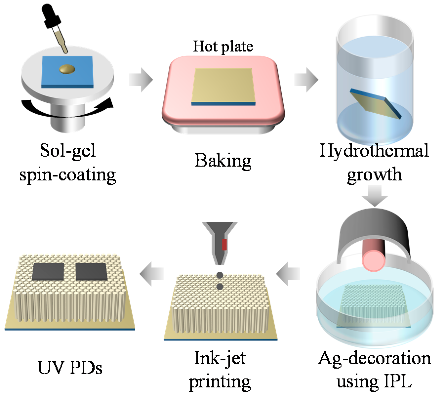
2.1. Synthesis of ZnO NWs

Figure 1 shows the fabrication process of the Ag-decorated ZnO NW UV PDs, including hydrothermal growth of ZnO NWs, Ag-decoration with IPL, and formation of electrodes using ink-jet printing. First, the ZnO NWs were synthesized using the hydrothermal method [8,37]. The Zn seed layer was prepared on a SiO2/Si substrate by sol-gel spin-coating of a mixture of zinc acetate dihydrate (0.5 M) and diethanolamine (0.5 M) in ethanol at 4000 rpm for 30 s. It was followed by heat-treatment at 350 °C for 30 min on a hotplate. Subsequently, ZnO NWs were grown hydrothermally at 90 °C for 4 h in a mixture of zinc nitrate hexahydrate (25 mM) and hexamethylenetetramine (25 mM) in deionized (DI) water.

2.2. Ag Decoration on as-Grown ZnO NWs

The as-grown ZnO NWs were decorated with Ag NPs using a facile and rapid IPL process. The SiO2/Si substrate on which ZnO NWs have been grown was dipped into silver nitrate (AgNO3) in DI water followed by IPL exposure. AgNO3 played the role of precursor for Ag NPs. The IPL equipment used in this study was composed of a Xenon flash lamp (P4128, Heraeus Co., Hanau, Germany), pulse controller (PSTEK Co., Gunpo, Korea), power supply, capacitors, and chilling unit. The concentrations of the Ag precursor and IPL irradiation energy were adopted as process variables in the Ag-decoration process. The IPL exposure was conducted with a single exposure, which lasted 8 ms. After the IPL process, the substrate was thoroughly rinsed with DI water.

2.3. Fabrication of UV PDs

The electrodes were fabricated on the Ag-decorated ZnO NWs by printing silver ink (DGP 40LT-13C, Advanced Nano Products Co., Sejong, Korea) with an ink-jet printer (DMP-2831, FUJIFILM Dimatix Co., Santa Clara, CA, USA) for UV PDs. The electrodes had dimensions of 2 mm × 2 mm and a channel length of 120 μm.

2.4. Characterization

Field-emission scanning electron microscopy (FE-SEM) (S-4800, Hitachi Co., Tokyo, Japan), high-resolution transmission electron microscopy (HR-TEM) (JEM-2100F, JEOL Co., Tokyo, Japan), and energy-dispersive X-ray spectroscopy (EDS) were used for morphological study of Ag-decorated ZnO NWs. X-ray photoelectron spectroscopy (XPS) (K-Alpha, Thermo Fisher Scientific Co., Waltham, MA, USA) and photoluminescence (PL) spectroscopy (LS55, PerkinElmer Co., Waltham, MA, USA) were used to analyze photocurrent characteristics. The performance of UV PDs was measured with a source meter (2634B, Keithley Instruments Co., Cleveland, OH, USA) using a UV light-emitting diode (LED) at a wavelength of 365 nm.

3. Results and Discussion

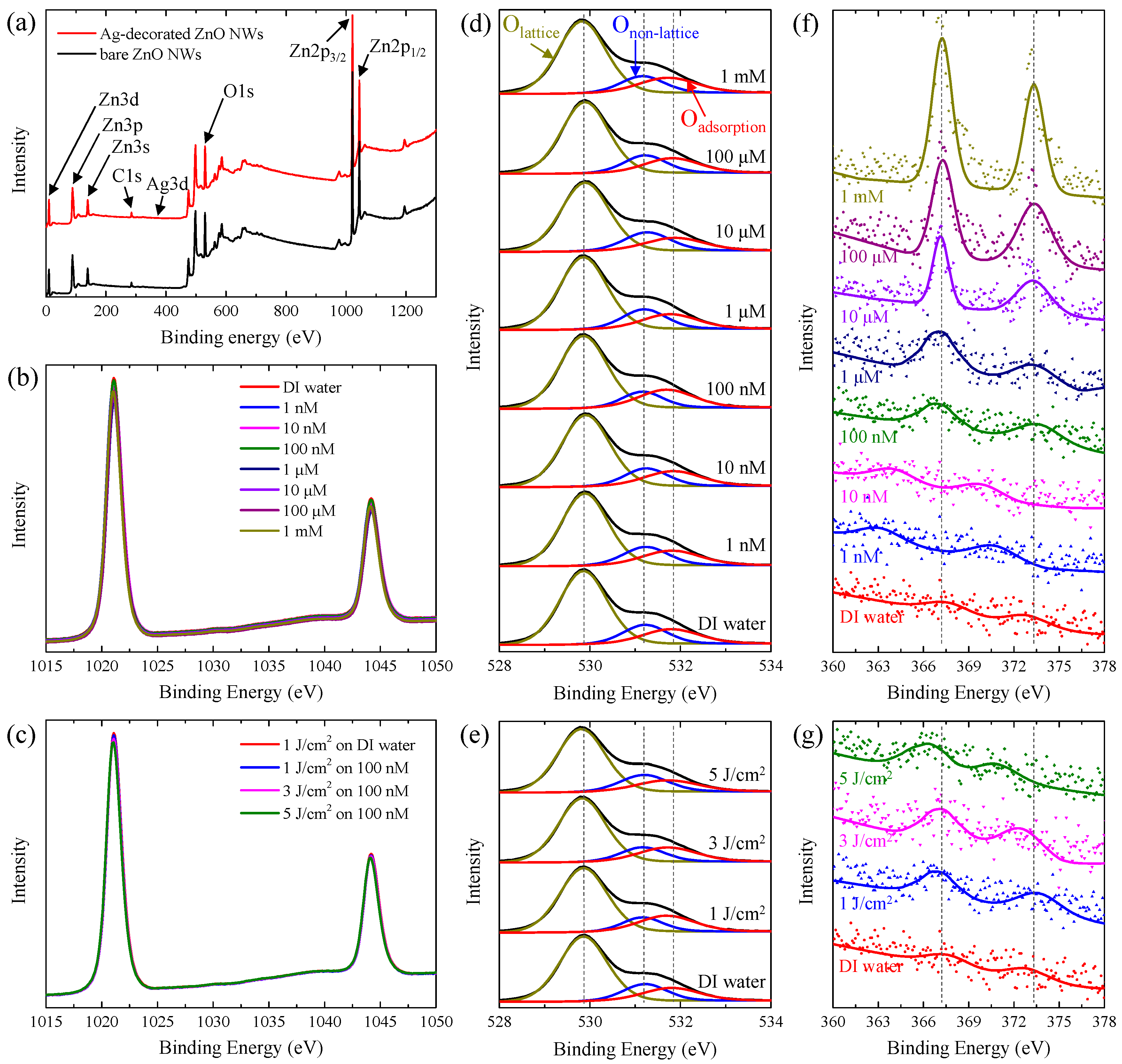
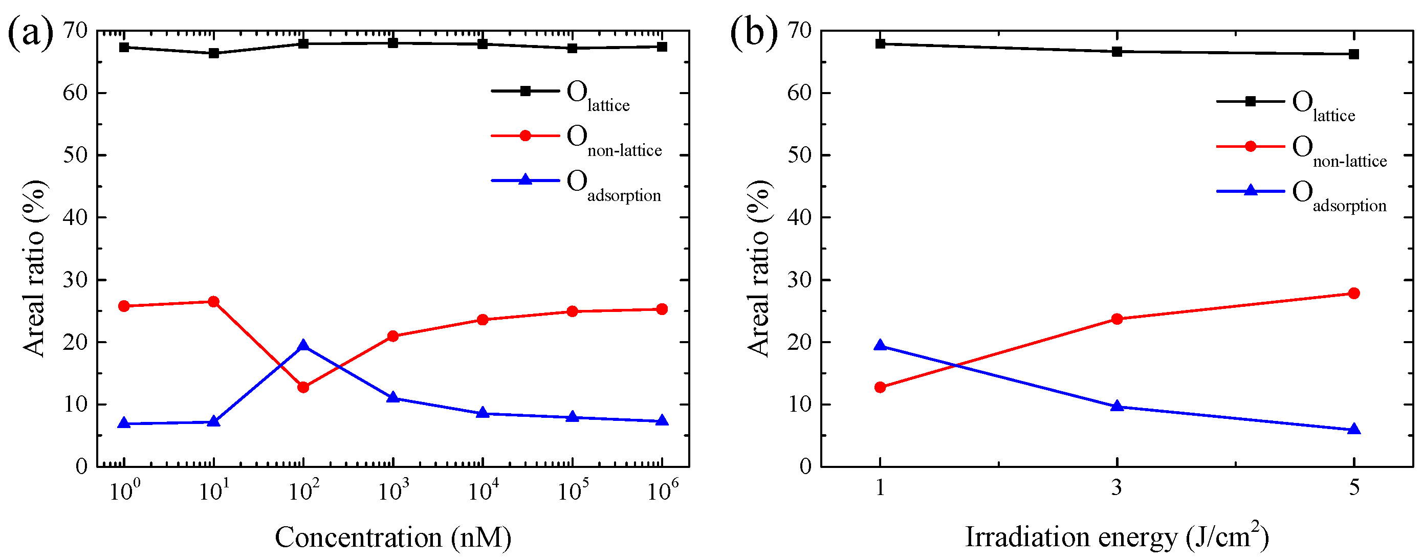
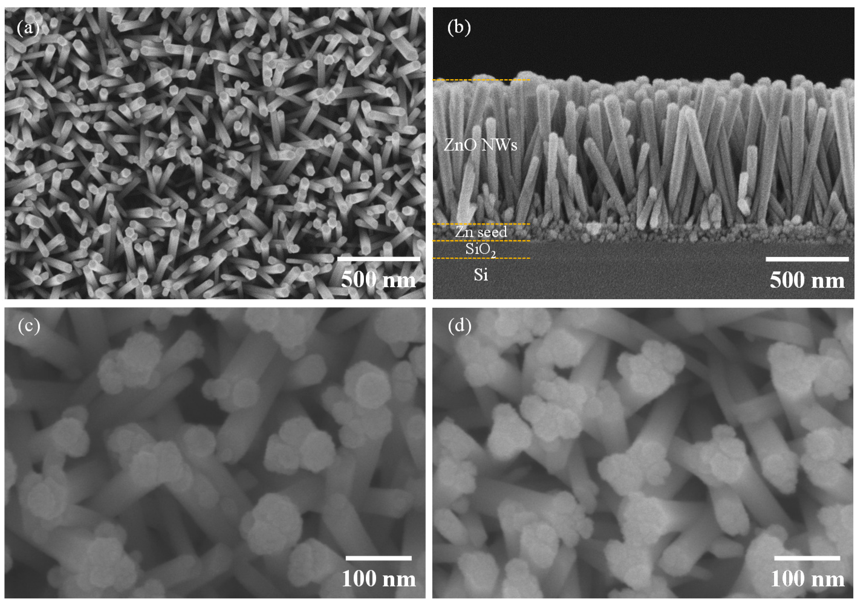
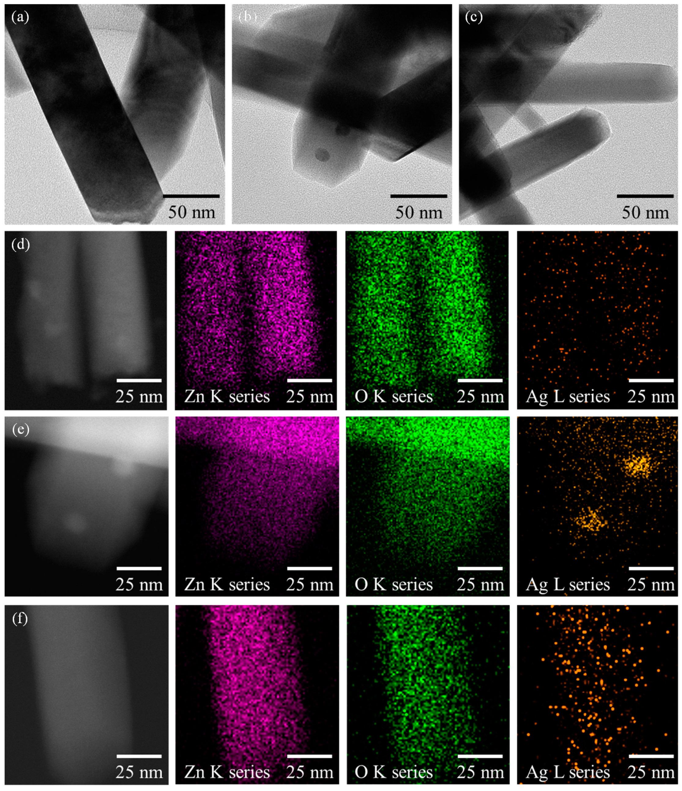
3.1. Ag-Decorated ZnO NWs

The SEM images of the hydrothermally as-grown ZnO NWs are shown in Figure 2. The ZnO NWs were grown vertically on the SiO2/Si substrate and are densely packed. They have an average diameter and length of 42 nm and 840 nm, respectively. The grown ZnO NWs exhibit the hexagonal wurtzite structure, as shown in Figure 2a. This observation is quite consistent with previous studies [8,9]. However, it was difficult to identify the decorated Ag NPs with SEM, which have been done with TEM. Figure 2c,d show ZnO NWs processed for 5 and 15 s in AgNO3 concentration of 1 mM at an IPL energy of 1 J/cm2 per pulse and frequency of 6 Hz, respectively. ZnO NWs are covered by Ag under excessive conditions. As the IPL irradiation time increases, the surface is covered with more Ag, which prevents a UV reaction on the surface.
Figure 3 displays TEM images and elemental maps of the as-grown and Ag-decorated ZnO NWs. Figure 3a−c shows the bright-field TEM images, in which the scale bars represent 50 nm. It is noted in Figure 3b, compared to the as-grown ZnO NW (Figure 3a), that several circular particles formed on the surface of ZnO NWs processed in a AgNO3 concentration of 100 nM at IPL irradiation energy of 1 J/cm2. However, no discernible particle shape was observed on the surface of the ZnO NWs processed in a AgNO3 concentration of 1 mM at 1 J/cm2 (Figure 3c). Elemental maps were acquired to confirm the distribution of Ag elements and demonstrated in Figure 3d−f. The Zn and O were homogeneously distributed with strong and high-density signals in all three conditions. However, this is not the case for the Ag, which was distributed differently under three conditions. The background signal from the as-grown ZnO nanowires is shown in Figure 3d, playing a role of control. The Ag was concentrated at the same position with the circular particles in the ZnO NWs processed in 100 nM at 1 J/cm2 (Figure 3e). The other part showed a slightly higher signal than the background in as-grown ZnO NWs. In the ZnO NWs, processed in 1 mM at 1 J/cm2, the Ag was evenly distributed on the surface of the ZnO NWs, as shown in Figure 3f. It is certain that the Ag signal is stronger than the background in the as-grown ZnO NWs. However, it does not build up large individual nanoparticles enough to be observed in TEM. It can be explained by the following reasons. The strong energy released from IPL induced nucleation from Ag+ on the surface of the ZnO NWs. When the concentration of AgNO3 was high, simultaneous nucleation occurred on all surfaces of the ZnO NWs. As shown in Figure 3f, circular particles were not yet formed, but Ag was evenly distributed on the surface. However, at the low concentration of AgNO3, nucleation was not uniform on the surface. Ag adsorbed on the surface of the ZnO NW was aggregated for nucleation and formed into circular particles, as shown in Figure 3e.
Figure 4 illustrates the binding energy among Ag, Zn, and O for the bare and Ag-decorated ZnO NWs. Figure 4a shows the full spectrum of the bare and ZnO NWs processed in 100 nM at 1 J/cm2. The spectrum was calibrated based on C 1s at Eb = 284.8 eV. The peaks from Zn and O were the same as the ones reported previously [26]. The peaks at 1021 and 1044 eV in Figure 4b,c are attributed to the Zn 2p3/2 and Zn 2p1/2, thus confirming that Zn exists in a divalent state. There was no change in the peak of Zn with respect to the concentration of AgNO3 solution and the IPL irradiation energy. It was confirmed that the Ag decoration process did not affect the binding energy of the Zn. The peak at 529.8 eV in Figure 4d,e was attributed to the O 1s. The spectrum of O 1s can be fitted to three Gaussian distributions representing different oxygen states. In general, the spectrum of O 1s can be represented by Olattice, Onon-lattice, and Oadsorption. These are O2 ions in the ZnO crystal lattice, O2 ions in the oxygen vacancy, and chemisorbed oxygen species on the surface, respectively [38]. Figure 5a,b demonstrate the areal ratio of O 1s with respect to the concentration of AgNO3 solution and IPL irradiation energy, respectively. The areal ratio for Olattice was almost constant with no change. The areal ratio of Oadsorption was maximized at 19.4% in ZnO NWs processed in 100 nM at 1 J/cm2, and 6.9% and 7.3% in ZnO NWs processed in 1 nM and 1 mM, respectively (Figure 5a). The ratio of Onon-lattice was relatively opposite to Oadsorption. The real ratio of Oadsorption decreased with increasing energy and was measured to be 5.9% in 100 nM at 5 J/cm2 (Figure 5b). Furthermore, in the result of energy change, the ratio of Onon-lattice showed relatively opposite trends. This means that the chemical activity of chemisorbed oxygen species increased, owing to the high conductivity and catalytic properties of Ag NPs [39,40,41,42]. In contrast, when the concentration further increased, the surface area exposed to the atmosphere was reduced by Ag, thereby reducing the amount of adsorbed oxygen species. The decrease in Oadsorption with increasing IPL irradiation energy could also be explained by the same reason. Figure 4f,g demonstrates the peaks at 367.3 and 373.3 eV from the Ag 3d3/2 and Ag 3d5/2 with respect to solution concentration and IPL energy, respectively. The scattered dots denote the raw data, while the line represents the fitted data. The difference (6.0 eV) in the binding energy indicates that Ag has a metallic nature [43]. The binding energy shifted significantly to a lower binding energy compared with the pure metallic Ag (368.2 eV and 374.2 eV) [44], which is attributed to the interaction between the Ag NPs and the ZnO NW. When the Ag NPs and the ZnO NW were attached together, they adjusted the location of the corresponding Fermi energy level to the same value. Thus, there are more free electrons than Ag NPs at the Fermi level. Given that the conduction band (CB) of the ZnO NW was empty, free electrons can tunnel into the CB, and the valence of the Ag increases. The binding energy of Ag+ was much lower than that of Ag0. Therefore, the binding energy of Ag 3d shifted to a lower binding energy [45,46]. The peak of Ag 3d decreased as the concentration and energy decreased, and the peak disappeared at 10 nM or less. The atomic percentage of Ag was calculated to be 0.174 at% in ZnO NWs processed in 1 mM at 1 J/cm2, 0.048 at% those processed in 100 nM at 1 J/cm2, and 0.055 at% in 100 nM at 5 J/cm2, respectively. Although Ag NPs were not observed in TEM, the Ag element exists on the surface of the ZnO NWs, which is confirmed by the elemental map result.
The PL spectra from ZnO NWs are demonstrated in Figure 6. Figure 6a presents the PL spectra of the bare ZnO NWs processed in DI water, and the Ag-decorated ZnO NWs processed in 100 nM at 1 J/cm2. The PL spectra of the ZnO NWs yielded a sharp peak intensity at 381 nm, mainly owing to the band–band exciton recombination associated with near-band edge emission [47,48,49]. Figure 6b,c displays the PL spectra with respect to AgNO3 concentration and IPL irradiation energy, respectively. As the concentration of AgNO3 solution increases, the intensity of PL increases up to 100 nM and then decreases again. Since the ZnO NW receives electrons from Ag NPs, the intensity of the PL increases. However, an excessive decoration process lowered the intensity of PL [50]. The PL peak decreased with an increase in the IPL irradiation energy, which is the same reason as in excessive decoration.

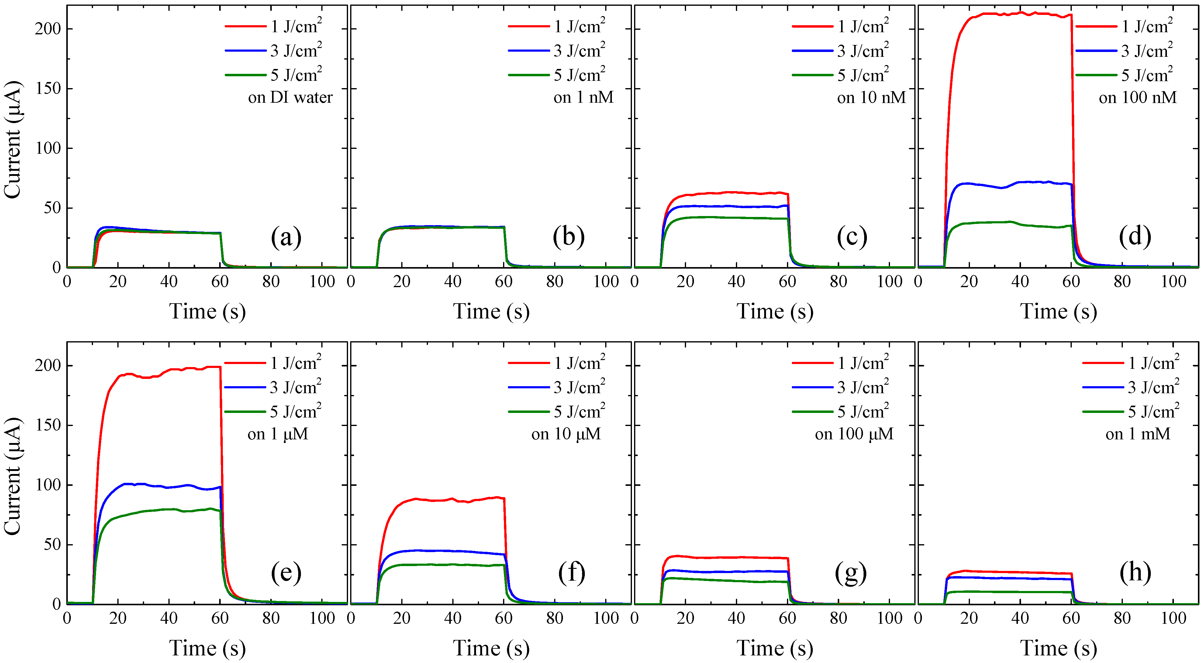
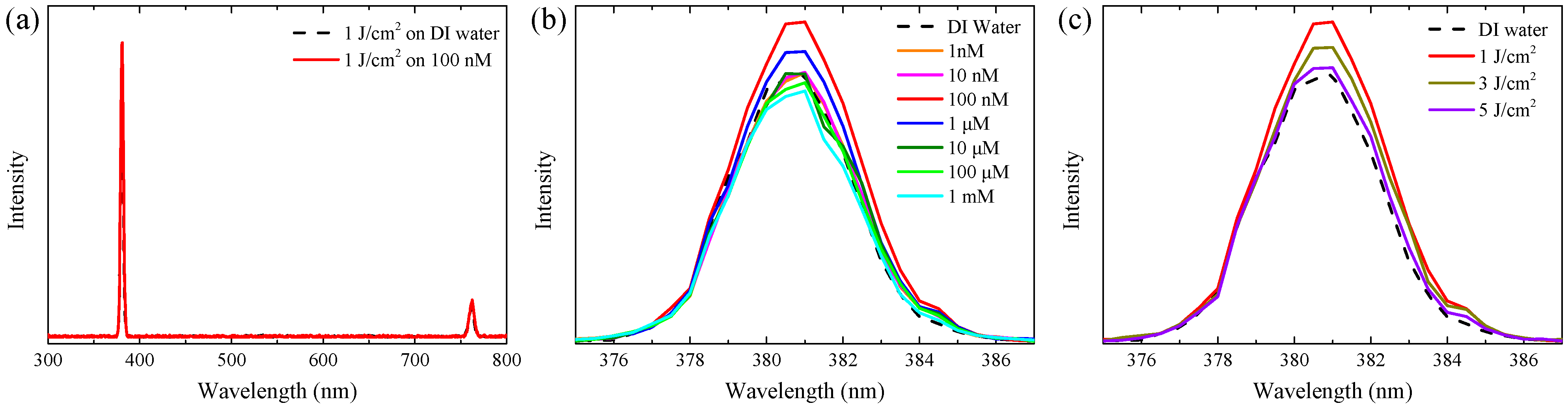
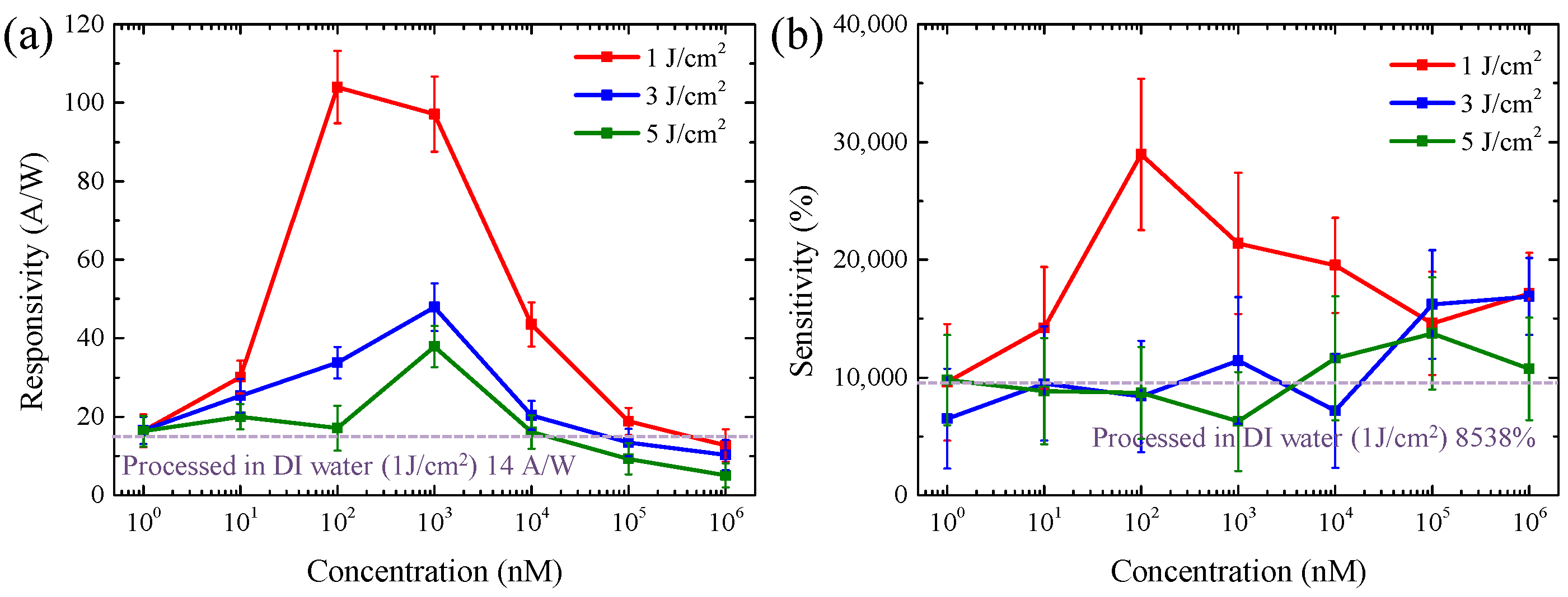
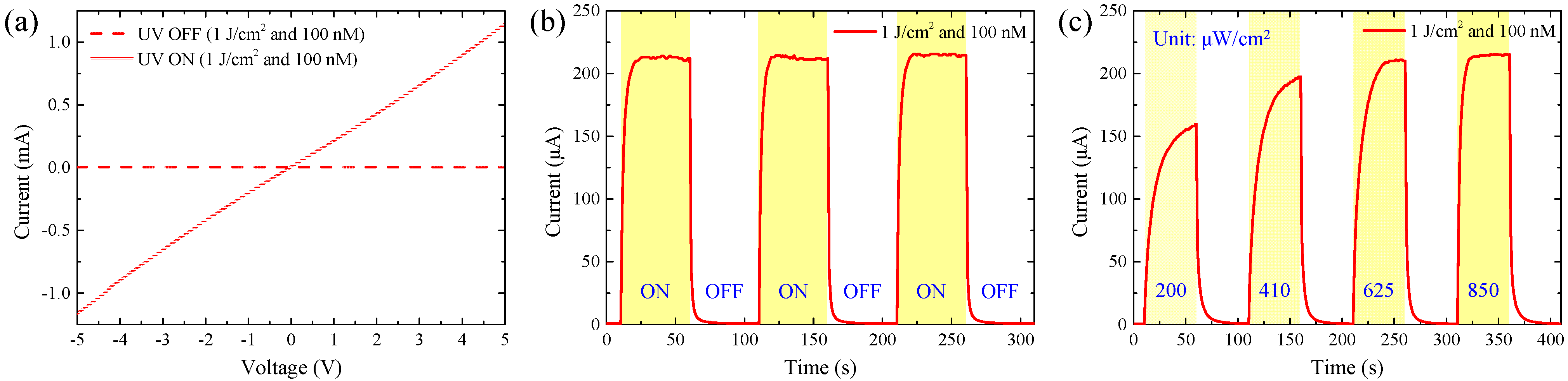
3.2. The Performance of Ag-Decorated ZnO NW UV PDs

Figure 7 shows the current measurement results at a bias voltage of 1 V. The UV PDs used here employed the bare and Ag-decorated ZnO NWs processed in DI water and various concentrations of AgNO3 solution. UV PDs were irradiated with a UV LED at a wavelength of 365 nm and a power density of 850 μW/cm2. The temporal response curves were obtained for a time of 50 s. The basic UV detection mechanism of the ZnO NWs is as follows. Electrons in the absence of UV moved to the center of the ZnO NW owing to the O2 molecules adsorbed on the surface of the ZnO NW. It forms a thin conduction channel in the center and a thick depletion region on the surface. In the presence of UV, the adsorbed O2 molecules were desorbed, and the ZnO NW conduction channel expanded, while the depletion region narrowed. The widened conduction channel increased the current flowing between electrodes. If the O2 molecules were not desorbed, the current should be saturated. When the UV was turned off again, O2 molecules were adsorbed on the surface, and the current decreased [7]. According to the experimental results, the highest light current was shown in the ZnO NWs processed in 100 nM at 1 J/cm2, as shown in Figure 7d. Figure 8 shows the responsivity and sensitivity with respect to the concentration of AgNO3 solution and IPL irradiation energy. The responsivity and sensitivity were calculated by the following equations [51,52]:
R = I l i g h t I d a r k P A ,
And:
S = I l i g h t I d a r k I d a r k × 100 ( % ) ,
where R is the responsivity, S is the sensitivity, Ilight is the light current, Idark is the dark current, A is the area between two electrodes, and P is the UV power. While the bare ZnO NWs have a responsivity of 14 A/W, the most responsivity was 104 A/W found in ZnO NWs processed in 100 nM at 1 J/cm2, which is 7.43 times increased, as shown in Figure 8a. Meanwhile, the ZnO NWs processed in 1 mM at 5 J/cm2 exhibited the lowest responsivity of 5.03 A/W, which was reduced by 64.1% compared to the bare ZnO NWs. The sensitivity was calculated to be the highest of 28,951% for ZnO NWs processed in 100 nM at 1 J/cm2, which is 3.39 times increased, as shown in Figure 8b. In addition, the external quantum efficiency (EQE), which is the ability of electrons generated by the excitation of photons, is defined as follows [52].
EQE = R × 1240 λ × 100 % ,
where λ is the wavelength of UV light. It depends on the responsivity (R) at the same wavelength (λ). At the largest responsivity, the EQE is calculated to be 35,312%. The increase in responsivity and sensitivity by the Ag decoration process results from the formed Ag NPs. The mechanism of UV detection by Ag NPs is described in Section 3.3. The decrease in responsivity decreased the photocurrent, which is the difference between the light current and dark current, owing to the decrease in oxygen species adsorbed on the surface of the ZnO NWs, like the decrease in the peak of Oadsorption of XPS. The performance of Ag-decorated ZnO by IPL was compared with the previous literature and is summarized in Table 1. The performance includes the responsivity, sensitivity, and response/recovery time of PDs based on the ZnO nanostructures decorated with metal NPs. It is confirmed that our study demonstrated a significant improvement compared to other literature.
Figure 9 shows the various performances of the UV PDs with ZnO NWs processed at optimal conditions. Figure 9a shows I-V curves on a voltage range of −5 to 5 V in the absence and presence of UV. It is noted that there was an ohmic contact between the Ag electrode and the Ag-decorated ZnO NWs. The conductivity of the channel between two electrodes was greatly increased in the presence of UVs. This was ascribed to an expanded conductive channel at the center of ZnO NWs. The results of the repeated measurements with a 50-s interval are shown in Figure 9b. The response/recovery time and repeatability were excellent. The time to reach 90% and 10% of the saturation state is defined as the response and recovery time, respectively. The response/recovery times of the Ag-decorated ZnO NWs PDs were and 5.6/2.2 s, respectively. The current was measured at increasing powers of UV with 200, 410, 625, and 850 μW/cm2, and is shown in Figure 9c. As the UV light power increases, the light current increases, and the response time decreases. The higher power of UV, the more O2 molecules desorbed from the surface of NWs. The decreased response time is attributed to the increased desorption rate of the O2 molecules on the surface.

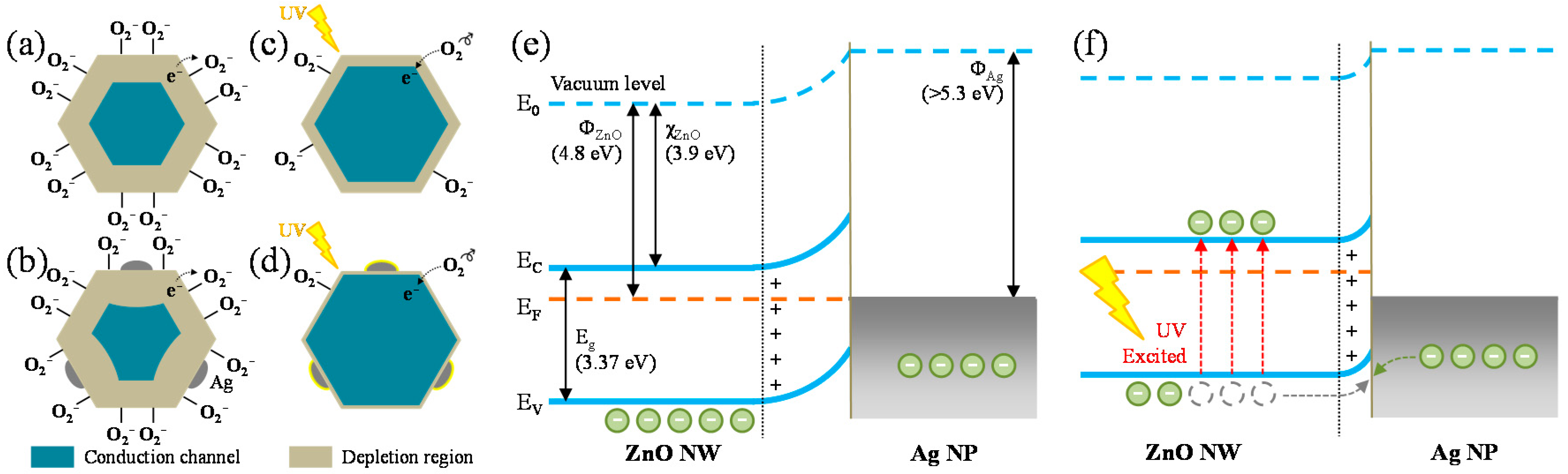
3.3. UV-Detection Mechanism

Herein, a detection mechanism is proposed for Ag-decorated ZnO NW UV PDs, as shown in Figure 10. Ag NPs play a dual role in UV PDs in enhancing the performance of UP PDs. At first, the catalytic properties of Ag NPs increase the chemical activity of the chemisorbed oxygen species, as shown in Figure 4d,e [39,40,41,42]. The increase in chemically activated oxygen species widens the depletion region in ZnO NWs, as shown in Figure 10b. More oxygen species are desorbed in the presence of Ag NPs upon exposure to UV light than in the absence of Ag NPs, resulting in more photocurrent in the presence of Ag NPs, as shown in Figure 10c,d. In general, ZnO NWs synthesized by the hydrothermal method are known to have a work function of 5.28 eV, an electron affinity of 4.35 eV, and a bandgap of 3.37 eV [64,65]. The work function of Ag is 4.26 eV; however, the smaller the NP size, the larger the work function [66,67]. The work function is found to be 5.3 eV when the Ag NP size decreases below 30 nm. Consequently, a Schottky barrier was formed at the interface of Ag NP and ZnO NW owing to the higher work function of Ag NP, as shown in Figure 10e [33,65,66,68]. This also leads to the narrowing of the conducting channel of the ZnO NWs, as shown in Figure 10b. The electrons were generated in the exposure of UV light, and the holes moved toward the Ag NPs owing to the Coulombic force [69]. Some holes were trapped at the interface, and the rest passed through the Schottky barrier and recombined with electrons, as shown in Figure 10f. This results in the narrowing of the depletion region. The photogenerated electrons were secured by the recombination of generated holes with the electrons from Ag NPs, which enhances lifetime. Additionally, Ag NPs enhance the light absorption efficiency by particle-induced light scattering [70]. It increases the number of photogenerated electron-hole pairs.

4. Conclusions

In conclusion, we employed a facile and rapid IPL method to decorate ZnO NWs with Ag NPs on the surfaces of the ZnO NWs grown vertically on the substrate. It was confirmed that Ag was successfully decorated on the ZnO NW surface through TEM, elemental maps, and XPS investigation. When the concentration of AgNO3 solution was lower than 100 nM, the Ag NPs were not formulated efficiently. The ZnO NWs processed in 100 nM at 1 J/cm2 exhibited the most superior decoration of Ag NPs along with the highest photocurrent. Further increase in the concentration and exposure energy of IPL resulted in a decrease in electrical performance of the ZnO NW PDs. The decoration process in this study boasts of extremely short (~8 ms) duration. Our results clearly indicate that the IPL process used in the current work is an efficient way to decorate Ag on ZnO NWs. Considering that it is difficult to improve the crystal quality of the ZnO NW grown at low temperatures, this can act as an exemplary guideline for the improvement of UV PD performance.

Author Contributions

Conceptualization, Y.N. and D.L.; methodology, Y.N.; software, H.L. and G.Y.K.; validation, Y.N., J.S., M.K. and D.L.; formal analysis, Y.N.; investigation, Y.N. and J.S.; resources, Y.N.; data curation, H.L. and G.Y.K.; writing—original draft preparation, Y.N.; writing—review and editing, M.K. and D.L.; visualization, Y.N.; supervision, D.L.; project administration, D.L.; funding acquisition, D.L. All authors have read and agreed to the published version of the manuscript.

Funding

This paper was supported by Konkuk University in 2018.

Data Availability Statement

The data presented in this study are available on request from the corresponding author.

Conflicts of Interest

The authors declare no conflict of interest.

References

  1. Schmidt-Mende, L.; MacManus-Driscoll, J.L. ZnO—nanostructures, defects, and devices. Mater. Today 2007, 10, 40–48. [Google Scholar] [CrossRef]
  2. Kong, Y.C.; Yu, D.P.; Zhang, B.; Fang, W.; Feng, S.Q. Ultraviolet-emitting ZnO nanowires synthesized by a physical vapor deposition approach. Appl. Phys. Lett. 2001, 78, 407–409. [Google Scholar] [CrossRef]
  3. Florica, C.; Preda, N.; Costas, A.; Zgura, I.; Enculescu, I. ZnO nanowires grown directly on zinc foils by thermal oxidation in air: Wetting and water adhesion properties. Mater. Lett. 2016, 170, 156–159. [Google Scholar] [CrossRef]
  4. Greene, L.E.; Law, M.; Goldberger, J.; Kim, F.; Johnson, J.C.; Zhang, Y.; Saykally, R.J.; Yang, P. Low-Temperature Wafer-Scale Production of ZnO Nanowire Arrays. Angew. Chem. Int. Ed. 2003, 42, 3031–3034. [Google Scholar] [CrossRef] [PubMed]
  5. Wang, J.; Gao, L. Hydrothermal synthesis and photoluminescence properties of ZnO nanowires. Solid State Commun. 2004, 132, 269–271. [Google Scholar] [CrossRef]
  6. Rühle, S.; van Vugt, L.K.; Li, H.Y.; Keizer, N.A.; Kuipers, L.; Vanmaekelbergh, D. Nature of Sub-Band Gap Luminescent Eigenmodes in a ZnO Nanowire. Nano Lett. 2008, 8, 119–123. [Google Scholar] [CrossRef] [PubMed] [Green Version]
  7. Park, J.; Lee, J.; Noh, Y.; Shin, K.-H.; Lee, D. Flexible ultraviolet photodetectors with ZnO nanowire networks fabricated by large area controlled roll-to-roll processing. J. Mater. Chem. C 2016, 4, 7948–7958. [Google Scholar] [CrossRef]
  8. Nam, D.; Park, J.; Park, S.; Min, Y.; Noh, Y.; Lee, D. High-density hydrothermal growth of zinc-oxide nanowires using printed resistive heater. Mater. Lett. 2015, 153, 29–32. [Google Scholar] [CrossRef]
  9. Lee, D.; Kim, T.; Park, S.; Lee, S.S.; Ko, S.H. Zinc Oxide Nanowire Forest for Pool Boiling Heat Transfer. Jpn. J. Appl. Phys. 2012, 51, 11PE11. [Google Scholar] [CrossRef]
  10. Song, K.; Noh, J.; Jun, T.; Jung, Y.; Kang, H.-Y.; Moon, J. Fully Flexible Solution-Deposited ZnO Thin-Film Transistors. Adv. Mater. 2010, 22, 4308–4312. [Google Scholar] [CrossRef]
  11. Jin, Y.; Wang, J.; Sun, B.; Blakesley, J.C.; Greenham, N.C. Solution-Processed Ultraviolet Photodetectors Based on Colloidal ZnO Nanoparticles. Nano Lett. 2008, 8, 1649–1653. [Google Scholar] [CrossRef]
  12. Mukhopadhyay, S.; Das, P.P.; Maity, S.; Ghosh, P.; Devi, P.S. Solution grown ZnO rods: Synthesis, characterization and defect mediated photocatalytic activity. Appl. Catal. B Environ. 2015, 165, 128–138. [Google Scholar] [CrossRef]
  13. Kakiuchi, K.; Hosono, E.; Kimura, T.; Imai, H.; Fujihara, S. Fabrication of mesoporous ZnO nanosheets from precursor templates grown in aqueous solutions. J. Sol-Gel Sci. Technol. 2006, 39, 63–72. [Google Scholar] [CrossRef]
  14. Xi, Y.; Hu, C.G.; Han, X.Y.; Xiong, Y.F.; Gao, P.X.; Liu, G.B. Hydrothermal synthesis of ZnO nanobelts and gas sensitivity property. Solid State Commun. 2007, 141, 506–509. [Google Scholar] [CrossRef]
  15. Xi, Y.; Song, J.; Xu, S.; Yang, R.; Gao, Z.; Hu, C.; Wang, Z.L. Growth of ZnO nanotube arrays and nanotube based piezoelectric nanogenerators. J. Mater. Chem. 2009, 19, 9260–9264. [Google Scholar] [CrossRef]
  16. Akhtar, N.; Metkar, S.K.; Girigoswami, A.; Girigoswami, K. ZnO nanoflower based sensitive nano-biosensor for amyloid detection. Mater. Sci. Eng. C 2017, 78, 960–968. [Google Scholar] [CrossRef]
  17. Al-Hardan, N.H.; Jalar, A.; Abdul Hamid, M.A.; Keng, L.K.; Ahmed, N.M.; Shamsudin, R. A wide-band UV photodiode based on n-ZnO/p-Si heterojunctions. Sens. Actuator A-Phys. 2014, 207, 61–66. [Google Scholar] [CrossRef]
  18. Tian, C.; Zhang, Q.; Wu, A.; Jiang, M.; Liang, Z.; Jiang, B.; Fu, H. Cost-effective large-scale synthesis of ZnO photocatalyst with excellent performance for dye photodegradation. Chem. Commun. 2012, 48, 2858–2860. [Google Scholar] [CrossRef] [PubMed]
  19. Wang, L.; Kang, Y.; Liu, X.; Zhang, S.; Huang, W.; Wang, S. ZnO nanorod gas sensor for ethanol detection. Sens. Actuator B-Chem. 2012, 162, 237–243. [Google Scholar] [CrossRef]
  20. Hatamie, A.; Khan, A.; Golabi, M.; Turner, A.P.F.; Beni, V.; Mak, W.C.; Sadollahkhani, A.; Alnoor, H.; Zargar, B.; Bano, S.; et al. Zinc Oxide Nanostructure-Modified Textile and Its Application to Biosensing, Photocatalysis, and as Antibacterial Material. Langmuir 2015, 31, 10913–10921. [Google Scholar] [CrossRef]
  21. Lu, M.-P.; Song, J.; Lu, M.-Y.; Chen, M.-T.; Gao, Y.; Chen, L.-J.; Wang, Z.L. Piezoelectric Nanogenerator Using p-Type ZnO Nanowire Arrays. Nano Lett. 2009, 9, 1223–1227. [Google Scholar] [CrossRef] [PubMed]
  22. Djurišić, A.B.; Leung, Y.H. Optical Properties of ZnO Nanostructures. Small 2006, 2, 944–961. [Google Scholar] [CrossRef] [PubMed]
  23. Klingshirn, C. ZnO: From basics towards applications. Phys. Status Solidi B 2007, 244, 3027–3073. [Google Scholar] [CrossRef]
  24. Dhara, S.; Giri, P.K. Enhanced UV photosensitivity from rapid thermal annealed vertically aligned ZnO nanowires. Nanoscale Res. Lett. 2011, 6, 504. [Google Scholar] [CrossRef] [Green Version]
  25. Zhang, J.; Que, W. Preparation and characterization of sol–gel Al-doped ZnO thin films and ZnO nanowire arrays grown on Al-doped ZnO seed layer by hydrothermal method. Sol. Energy Mater. Sol. Cells 2010, 94, 2181–2186. [Google Scholar] [CrossRef]
  26. Jiang, H.; Liu, S.; Liang, L.; Lu, W. Oxygen plasma assisted enhanced photoresponse of ZnO nanowires fabricated by catalyst-free chemical vapor deposition. RSC Adv. 2018, 8, 28928–28933. [Google Scholar] [CrossRef] [Green Version]
  27. Wagata, H.; Ohashi, N.; Katsumata, K.-i.; Segawa, H.; Wada, Y.; Yoshikawa, H.; Ueda, S.; Okada, K.; Matsushita, N. An aqueous solution process and subsequent UV treatment for highly transparent conductive ZnO films. J. Mater. Chem. 2012, 22, 20706–20712. [Google Scholar] [CrossRef]
  28. Zhang, X.; Zhao, J.; Wang, S.; Dai, H.; Sun, X. Shape-dependent localized surface plasmon enhanced photocatalytic effect of ZnO nanorods decorated with Ag. Int. J. Hydrogen Energy 2014, 39, 8238–8245. [Google Scholar] [CrossRef]
  29. Xiang, Q.; Meng, G.; Zhang, Y.; Xu, J.; Xu, P.; Pan, Q.; Yu, W. Ag nanoparticle embedded-ZnO nanorods synthesized via a photochemical method and its gas-sensing properties. Sens. Actuator B-Chem. 2010, 143, 635–640. [Google Scholar] [CrossRef]
  30. Ko, Y.H.; Yu, J.S. Silver nanoparticle decorated ZnO nanorod arrays on AZO films for light absorption enhancement. Phys. Status Solidi A 2012, 209, 297–301. [Google Scholar] [CrossRef]
  31. Tang, H.; Meng, G.; Huang, Q.; Zhang, Z.; Huang, Z.; Zhu, C. Arrays of Cone-Shaped ZnO Nanorods Decorated with Ag Nanoparticles as 3D Surface-Enhanced Raman Scattering Substrates for Rapid Detection of Trace Polychlorinated Biphenyls. Adv. Funct. Mater. 2012, 22, 218–224. [Google Scholar] [CrossRef]
  32. Slimi, B.; Ben Assaker, I.; Kriaa, A.; Marí, B.; Chtourou, R. One-step electrodeposition of Ag-decorated ZnO nanowires. J. Solid State Electrochem. 2017, 21, 1253–1261. [Google Scholar] [CrossRef]
  33. Tzeng, S.-K.; Hon, M.-H.; Leu, I.-C. Improving the Performance of a Zinc Oxide Nanowire Ultraviolet Photodetector by Adding Silver Nanoparticles. J. Electrochem. Soc. 2012, 159, H440–H443. [Google Scholar] [CrossRef]
  34. Han, Z.; Li, S.; Chu, J.; Chen, Y. Controlled growth of well-aligned ZnO nanowire arrays using the improved hydrothermal method. J. Semicond. 2013, 34, 063002. [Google Scholar] [CrossRef]
  35. Zhang, Z.; Lv, Y.; Yan, J.; Hui, D.; Yun, J.; Zhai, C.; Zhao, W. Uniform ZnO nanowire arrays: Hydrothermal synthesis, formation mechanism and field emission performance. J. Alloys Compd. 2015, 650, 374–380. [Google Scholar] [CrossRef]
  36. Chang, C.W.; Wu, H.T.; Huang, S.H.; Chen, C.K.; Un, I.W.; Yen, T.J. Single-crystalline heterostructure of ZnO nanowire arrays on large Ag microplates and its photocatalytic activity. Acta Mater. 2013, 61, 6993–6999. [Google Scholar] [CrossRef]
  37. Chen, K.J.; Hung, F.Y.; Chang, S.J.; Young, S.J. Optoelectronic characteristics of UV photodetector based on ZnO nanowire thin films. J. Alloys Compd. 2009, 479, 674–677. [Google Scholar] [CrossRef]
  38. Lai, Y.; Xin, P.; Cheng, S.; Yu, J.; Zheng, Q. Plasma enhanced multistate storage capability of single ZnO nanowire based memory. Appl. Phys. Lett. 2015, 106, 031603. [Google Scholar] [CrossRef]
  39. Yan, S.; Li, Z.; Li, H.; Wu, Z.; Wang, J.; Shen, W.; Fu, Y.Q. Ultra-sensitive room-temperature H2S sensor using Ag–In2O3 nanorod composites. J. Mater. Sci. 2018, 53, 16331–16344. [Google Scholar] [CrossRef]
  40. Chen, M.; Wang, H.; Hu, J.; Zhang, Y.; Li, K.; Zhang, D.; Zhou, S.; Zhang, J.; Zhu, Z.; Liu, Q. Near-Room-Temperature Ethanol Gas Sensor Based on Mesoporous Ag/Zn–LaFeO3 Nanocomposite. Adv. Mater. Interfaces 2019, 6, 1801453. [Google Scholar] [CrossRef] [Green Version]
  41. Zhang, X.; Song, D.; Liu, Q.; Chen, R.; Hou, J.; Liu, J.; Zhang, H.; Yu, J.; Liu, P.; Wang, J. Designed synthesis of Ag-functionalized Ni-doped In2O3 nanorods with enhanced formaldehyde gas sensing properties. J. Mater. Chem. C 2019, 7, 7219–7229. [Google Scholar] [CrossRef]
  42. Xu, L.; Xing, R.; Song, J.; Xu, W.; Song, H. ZnO–SnO2 nanotubes surface engineered by Ag nanoparticles: Synthesis, characterization, and highly enhanced HCHO gas sensing properties. J. Mater. Chem. C 2013, 1, 2174–2182. [Google Scholar] [CrossRef]
  43. Li, F.; Wu, S.; Zhang, L.; Li, Z. Ag nanoparticles decorated ZnO nanoarrays with enhanced surface-enhanced Raman scattering and field emission property. J. Mater. Sci. Mater. Electron. 2017, 28, 16233–16238. [Google Scholar] [CrossRef]
  44. Liu, H.; Liu, H.; Yang, J.; Zhai, H.; Liu, X.; Jia, H. Microwave-assisted one-pot synthesis of Ag decorated flower-like ZnO composites photocatalysts for dye degradation and NO removal. Ceram. Int. 2019, 45, 20133–20140. [Google Scholar] [CrossRef]
  45. Chen, C.; Zheng, Y.; Zhan, Y.; Lin, X.; Zheng, Q.; Wei, K. Enhanced Raman scattering and photocatalytic activity of Ag/ZnO heterojunction nanocrystals. Dalton Trans. 2011, 40, 9566–9570. [Google Scholar] [CrossRef]
  46. Zheng, Y.; Zheng, L.; Zhan, Y.; Lin, X.; Zheng, Q.; Wei, K. Ag/ZnO Heterostructure Nanocrystals:  Synthesis, Characterization, and Photocatalysis. Lnorg. Chem. 2007, 46, 6980–6986. [Google Scholar] [CrossRef] [PubMed]
  47. Musa, I.; Qamhieh, N.; Mahmoud, S.T. Synthesis and length dependent photoluminescence property of zinc oxide nanorods. Results Phys. 2017, 7, 3552–3556. [Google Scholar] [CrossRef]
  48. Khan, W.; Khan, F.; Ajmal, H.M.; Huda, N.U.; Kim, J.H.; Kim, S.-D. Evolution of Structural and Optical Properties of ZnO Nanorods Grown on Vacuum Annealed Seed Crystallites. Nanomaterials 2018, 8, 68. [Google Scholar] [CrossRef] [PubMed] [Green Version]
  49. Jane, P.; Mariano, G.; Ilaria, R.; Luca De, S.; Ivo, R. Photoluminescence characterization of ZnO nanowires functionalization. In Proceedings of the SPIE Optics + Optoelectronics, Prague, Czech Republic, 13–16 April 2015. [Google Scholar]
  50. Liang, Y.-C.; Lo, Y.-R.; Wang, C.-C.; Xu, N.-C. Shell Layer Thickness-Dependent Photocatalytic Activity of Sputtering Synthesized Hexagonally Structured ZnO-ZnS Composite Nanorods. Materials 2018, 11, 87. [Google Scholar] [CrossRef] [Green Version]
  51. Abdulrahman, A.F.; Ahmed, S.M.; Barzinjy, A.A.; Hamad, S.M.; Ahmed, N.M.; Almessiere, M.A. Fabrication and Characterization of High-Quality UV Photodetectors Based ZnO Nanorods Using Traditional and Modified Chemical Bath Deposition Methods. Nanomaterials 2021, 11, 677. [Google Scholar] [CrossRef]
  52. Li, M.-Y.; Yu, M.; Su, D.; Zhang, J.; Jiang, S.; Wu, J.; Wang, Q.; Liu, S. Ultrahigh Responsivity UV Photodetector Based on Cu Nanostructure/ZnO QD Hybrid Architectures. Small 2019, 15, 1901606. [Google Scholar] [CrossRef]
  53. Liu, Y.; Zhang, X.; Su, J.; Li, H.; Zhang, Q.; Gao, Y. Ag nanoparticles@ZnO nanowire composite arrays: An absorption enhanced UV photodetector. Opt. Express 2014, 22, 30148–30155. [Google Scholar] [CrossRef] [PubMed]
  54. Zhao, X.; Wang, F.; Shi, L.; Wang, Y.; Zhao, H.; Zhao, D. Performance enhancement in ZnO nanowire based double Schottky-barrier photodetector by applying optimized Ag nanoparticles. RSC Adv. 2016, 6, 4634–4639. [Google Scholar] [CrossRef]
  55. Yang, C.; Yu, H.; Su, Y.; Chuang, M.; Hsiao, C.; Kao, T. Noise Properties of Ag Nanoparticle-Decorated ZnO Nanorod UV Photodetectors. IEEE Photonics Technol. Lett. 2016, 28, 379–382. [Google Scholar] [CrossRef]
  56. Dinh, T.M.; Huynh, H.Q.; Mai, T.M.N.; Truong, H.S.; Luong, H.N.; Nguyen, N.P.; Tran, C.K.; Phan, B.T.; Dang, V.Q. Enhancing the performance of photodetectors based on ZnO nanorods decorated with Ag nanoparticles. Semicond. Sci. Technol. 2021, 36, 045009. [Google Scholar] [CrossRef]
  57. Wang, X.; Liu, K.; Chen, X.; Li, B.; Jiang, M.; Zhang, Z.; Zhao, H.; Shen, D. Highly Wavelength-Selective Enhancement of Responsivity in Ag Nanoparticle-Modified ZnO UV Photodetector. ACS Appl. Mater. Interfaces 2017, 9, 5574–5579. [Google Scholar] [CrossRef]
  58. Wang, H.-C.; Hong, Y.; Chen, Z.; Lao, C.; Lu, Y.; Yang, Z.; Zhu, Y.; Liu, X. ZnO UV Photodetectors Modified by Ag Nanoparticles Using All-Inkjet-Printing. Nanoscale Res. Lett. 2020, 15, 176. [Google Scholar] [CrossRef]
  59. Khan, R.; Uthirakumar, P.; Kim, T.H.; Lee, I.-H. Enhanced photocurrent performance of partially decorated Au nanoparticles on ZnO nanorods based UV photodetector. Mater. Res. Bull. 2019, 115, 176–181. [Google Scholar] [CrossRef]
  60. Zhang, H.; Zhao, Y.; Geng, X.; Huang, Y.; Li, Y.; Liu, H.; Liu, Y.; Li, Y.; Wang, X.; Tian, H.; et al. Au Nanoparticles-Decorated Surface Plasmon Enhanced ZnO Nanorods Ultraviolet Photodetector on Flexible Transparent Mica Substrate. IEEE J. Electron Devices Soc. 2019, 7, 196–202. [Google Scholar] [CrossRef]
  61. Gogurla, N.; Sinha, A.K.; Santra, S.; Manna, S.; Ray, S.K. Multifunctional Au-ZnO Plasmonic Nanostructures for Enhanced UV Photodetector and Room Temperature NO Sensing Devices. Sci. Rep. 2014, 4, 6483. [Google Scholar] [CrossRef] [Green Version]
  62. Lu, J.; Xu, C.; Dai, J.; Li, J.; Wang, Y.; Lin, Y.; Li, P. Improved UV photoresponse of ZnO nanorod arrays by resonant coupling with surface plasmons of Al nanoparticles. Nanoscale 2015, 7, 3396–3403. [Google Scholar] [CrossRef] [PubMed]
  63. Jayalakshmi, G.; Saravanan, K. High-performance UV surface photodetector based on plasmonic Ni nanoparticles-decorated hexagonal-faceted ZnO nanorod arrays architecture. J. Mater. Sci. Mater. Electron. 2020, 31, 5710–5720. [Google Scholar] [CrossRef]
  64. Subha, P.P.; Jayaraj, M.K. Enhanced room temperature gas sensing properties of low temperature solution processed ZnO/CuO heterojunction. BMC Chem. 2019, 13, 4. [Google Scholar] [CrossRef] [Green Version]
  65. Li, X.; Chen, Y.; Kumar, A.; Mahmoud, A.; Nychka, J.A.; Chung, H.-J. Sponge-Templated Macroporous Graphene Network for Piezoelectric ZnO Nanogenerator. ACS Appl. Mater. Interfaces 2015, 7, 20753–20760. [Google Scholar] [CrossRef] [PubMed]
  66. Schnippering, M.; Carrara, M.; Foelske, A.; Kötz, R.; Fermín, D.J. Electronic properties of Ag nanoparticle arrays. A Kelvin probe and high resolution XPS study. PCCP 2007, 9, 725–730. [Google Scholar] [CrossRef]
  67. Kumatani, A.; Li, Y.; Darmawan, P.; Minari, T.; Tsukagoshi, K. On Practical Charge Injection at the Metal/Organic Semiconductor Interface. Sci. Rep. 2013, 3, 1026. [Google Scholar] [CrossRef]
  68. Yang, F.; Zheng, M.; Zhao, L.; Guo, J.; Zhang, B.; Gu, G.; Cheng, G.; Du, Z. The high-speed ultraviolet photodetector of ZnO nanowire Schottky barrier based on the triboelectric-nanogenerator-powered surface-ionic-gate. Nano Energy 2019, 60, 680–688. [Google Scholar] [CrossRef]
  69. Liu, K.; Sakurai, M.; Liao, M.; Aono, M. Giant Improvement of the Performance of ZnO Nanowire Photodetectors by Au Nanoparticles. J. Phys. Chem. C 2010, 114, 19835–19839. [Google Scholar] [CrossRef]
  70. Atwater, H.A.; Polman, A. Plasmonics for improved photovoltaic devices. Nat. Mater. 2010, 9, 205–213. [Google Scholar] [CrossRef]
Figure 1. Schematic of fabrication for the Ag-decorated ZnO NW UV PDs.
Chemosensors 09 00321 g001
Figure 2. SEM images of (a) top view and (b) cross-sectional view of as-grown ZnO NWs and ZnO NWs processed for (c) 5 and (d) 15 s under excessive conditions.
Chemosensors 09 00321 g002
Figure 3. TEM images of (a) the as-grown ZnO NWs and the Ag-decorated ZnO NWs processed at IPL energy of 1 J/cm2 and AgNO3 concentration of (b) 100 nM, and (c) 1 mM. Elemental map image of (d) the as-grown ZnO NWs and the Ag-decorated ZnO NWs at IPL energy of 1 J/cm2 and AgNO3 concentration of (e) 100 nM, and (f) 1 mM.
Chemosensors 09 00321 g003
Figure 4. XPS of the bare and Ag-decorated ZnO NWs: (a) survey; (b,c) Zn 2p spectrum; (d,e) O 1s spectrum; and (f,g) Ag 3d spectrum. (b,d,f) Plots at different concentrations, (c,e,g) plots at different IPL irradiation energies.
Chemosensors 09 00321 g004
Figure 5. Areal ratio of O 1s in XPS with respect to (a) AgNO3 concentration and (b) IPL irradiation energy.
Chemosensors 09 00321 g005
Figure 6. PL spectra of the bare and Ag-decorated ZnO NWs: (a) full spectra and peak at 381 nm at different (b) AgNO3 concentrations and (c) IPL irradiation energy.
Chemosensors 09 00321 g006
Figure 7. Photocurrent in UV PDs empolying the bare and Ag-decorated ZnO NWs processed in (a) DI water and AgNO3 concentration of (b) 1 nM, (c) 10 nM, (d) 100 nM, (e) 1 μM, (f) 10 μM, (g) 100 μM, and (h) 1 mM.
Chemosensors 09 00321 g007
Figure 8. (a) Responsivity and (b) sensitivity with respect to AgNO3 concentration and IPL irradiation energy.
Chemosensors 09 00321 g008
Figure 9. (a) I-V curves in absence and presence of UV, and temporal variations of (b) repeatability, and (c) UV light energy measurements of Ag-decorated the ZnO NWs.
Chemosensors 09 00321 g009
Figure 10. Schematic of the UV detection mechanism of the Ag-decorated ZnO NW PDs: Depletion/conduction channel in (a,c) bare ZnO NWs and (b,d) Ag-decorated ZnO NWs in a dark state and upon UV exposure, energy-band diagrams for the Ag/ZnO heterojunction (e) in a dark state and (f) upon UV exposure.
Chemosensors 09 00321 g010
Table 1. Comparison of performances of ZnO nanostructure UV PDs decorated with metal NPs.
MaterialsBias Voltage
(V)
Wavelength
(nm)
Responsivity
(A/W)
Sensitivity
(%)
Response/
Recovery Time
(s)
Ref.
ZnO NWs13651485384.3/3.2This work
Ag NPs-ZnO NWs136510428,9515.6/2.2This work
Ag NPs-ZnO NWs5365-~89701.02/15.5[53]
Ag NPs-ZnO NWs0.5365-239,9924/36[33]
Ag NPs-ZnO NWs53654.91 × 106-6.3/26.3[54]
Ag NPs-ZnO NRs0.238012.4--[55]
Ag NPs-ZnO NRs54006.52 × 10−3--/157.77[56]
Ag NPs-ZnO TFs53802.86-15/330[57]
Ag NPs-ZnO TFs20365~0.04-3.89/4.38[58]
Au NPs-ZnO NRs3365-~4385-[59]
Au NPs-ZnO NRs136570--[60]
Au NPs-ZnO NSs5325~60--[61]
Al NPs-ZnO NRs5325~1.65-0.03/0.035[62]
Ni NPs-ZnO NRs13250.124-Prompt rise/rapid fall[63]
Publisher’s Note: MDPI stays neutral with regard to jurisdictional claims in published maps and institutional affiliations.

