Article

Laser Illumination Adjustments for Signal-to-Noise Ratio and Spatial Resolution Enhancement in Static 2D Chemical Images of NbOx/IGZO/ITO/Glass Light-Addressable Potentiometric Sensors

1
Department of Electronic Engineering, Chang-Gung University, Taoyuan 33302, Taiwan
2
Mechanical Engineering Department, Indian Institute of Technology Kharagpur, Kharagpur 721302, India
3
Department of Neurosurgery, Chang Gung Memorial Hospital, Linkou, Taoyuan 33305, Taiwan
4
The College of Medicine, Chang Gung University, Taoyuan 33302, Taiwan
5
Institute of Electro-Optical Engineering, Chang Gung University, Taoyuan 33302, Taiwan
6
Biosensor Group, Biomedical Engineering Research Center, Chang Gung University, Taoyuan 33302, Taiwan
7
Department of General Surgery, Chang Gung Memorial Hospital, Linkou, Taoyuan 33305, Taiwan
8
Artificial Intelligence Research Center, Chang-Gung University, Taoyuan 33302, Taiwan
*
Author to whom correspondence should be addressed.
Chun-Hui Chen, Neelanjan Akuli, and Yu-Jen Lu contributed equally to this work.
Chemosensors 2021, 9(11), 313; https://doi.org/10.3390/chemosensors9110313
Submission received: 2 September 2021 / Revised: 17 October 2021 / Accepted: 1 November 2021 / Published: 4 November 2021
(This article belongs to the Section Electrochemical Devices and Sensors)

Abstract

:
In a previous study, a thin In-Ga-Zn-oxide light addressable potentiometric sensor (IGZO LAPS) was indicated to have the advantages of low interference from ambient light, a high photocurrent and transfer efficiency, and a low cost. However, illumination optimization to obtain two-dimensional (2D) chemical images with better spatial resolutions has not been fully investigated. The trigger current and AC-modulated frequency of a 405-nm laser used to illuminate the fabricated IGZO LAPS were modified to check the photocurrent of the sensing area and SU8–2005 masking area, obtaining spatial resolution-related functions for the first time. The trigger current of illumination was adjusted from 0.020 to 0.030 A to compromise between an acceptable photocurrent and the integrity of the SU8–2005 masking layer. The photocurrent (PC) and differential photocurrent (DPC) versus scanning length (SL) controlled by an X-Y stage were used to check the resolved critical dimensions (CDs). The difference between resolved CD and optically measured CD (e.g., delta CD) measured at an AC frequency of 500 Hz revealed overall smaller values, supporting precise measurement in 2D imaging. The signal-to-noise ratio (SNR) has an optimized range of 2.0 to 2.15 for a better resolution for step spacings of both 10 and 2 μm in the scanning procedure to construct static 2D images. Under illumination conditions with a trigger current of 0.025 A and at an AC frequency of 500 Hz, the spatial resolution can be reduced to 10 μm from the pattern width of 6 μm. This developed methodology provides a quantitative evaluation with further optimization in spatial resolution without an extra cost for applications requiring a high spatial resolution, such as single-cell activity.

1. Introduction

Lab-on-a-chip systems, including microfluidic, miniature sensors and actuators, have proven to be promising platforms for rapid screening and point-of-care testing (POCT) applications in recent years [1,2,3]. To provide additional information, a sensor array with the advantages of stability, a small volume and a low cost is preferred. However, the conventional sensor array cannot be easily or flexibly integrated into the whole LOC system due to the volume limitation of microfluidics [4]. The individual sensor at a fixed position defined by the manufacturer highly constrains the mass information availability and sensing flexibility to match real applications, especially biomedical targets. For example, detection targets with uncertain landing properties on the sensing surface could lead to a very low capture rate and follow an undetectable signal such as single cell or very low concentration antigen sensing applications [5]. Therefore, spatially resolved mapping of the molecular species or cell-functionalized areas provided by sensor arrays could be a target with which current limitations can be overcome. In the meantime, the stability and reproducibility of the sensor array are generally considered as key requirements before commercialization [5,6]. Therefore, field-effect sensors could be one of the most promising candidates due to their compatibility with the semiconductor industry and relative advantages in fabrication and miniaturization [7,8]. As the most representative commercial product (e.g., Ion Torrent, Thermo Fisher Scientific Inc., in the United States of America (U.S.), a sensor array made by extended-gate field-effect transistors (EGFETs) with a specific readout circuit are proposed for next-generation DNA sequencing [9,10]. The chips made for Ion Torrent with a readout circuit induce an extra cost, which is a burden of disposable applications. One of the promising field-effect sensors, named light-addressable potentiometric sensors (LAPSs) [11], derived from electrolyte-insulator-semiconductor (EIS) structures [12] and ion-sensitive field-effect transistors (ISFETs) [13,14], have natural merits in array-like applications compared to EGFETs, EIS structures, ISFETs and CMOS ion image sensors [15], such as their simple fabrication and ability to handle two-dimensional (2D) chemical images composed of light-addressed measurement pixels [11,12,16,17,18]. Once the additional active area for AC modulated illumination is opened from the backside contact metal layer from the EIS structure, the LAPS structure can be simply fabricated [12,16]. With illumination into LAPS, penetrated photons can be absorbed by the semiconductor layer, and extra carriers (electron-hole pairs) are generated and diffused. At the same time, an electrical field generated by the bias voltage is applied between the reference electrode in the electrolyte and a backside contact to the semiconductor layer can drive the generated electron-hole pair separation, especially when operated in the depletion mode. In the general operation of LAPSs, illumination is turned on during the positive half of the AC-modulation period, which can generate a gradient of carrier concentrations (e.g., electrons) in the semiconductor, and the diffusion of extra carriers can induce a transient current (e.g., AC photocurrent). Then, illumination is turned off during the negative half of the AC-modulation period, and excess holes inside the depletion layer are removed by recombination, resulting in a transient current in the reverse direction. Under a given voltage bias, the level of the generated AC photocurrent is determined by the operation mode of the LAPS, especially the relative field-effect-induced depletion mode. This typical photocurrent versus bias voltage curve was observed with a parallel shift due to surface-binding charges provided by the different pH or ion concentrations of the electrolyte. A linear correlation between the bias voltage shift and the pH value of the electrolyte is naturally found as a pH-sensing response [14,18]. Consequently, with this common behavior, a fabricated LAPS can be considered a pH or ion concentration sensor in practice. Furthermore, photocurrents aligned with their coordinates can also be collected by systematic arrangement with illumination addressability in the LAPS readout instrument to generate two-dimensional (2D) chemical imaging [18,19] or volume information of the sensor array [20,21]. Compared to the conventional electrode/sensor array with a predefined sensing location, LAPS based on the virtual electrode/sensor defined by scanning has a high flexibility to modify measurement pixels, which is beneficial in real applications such as the uncertain location in vivo measurement of cells. To have a multipixel sensor array, EIS structures, ISFETs and complementary metal–oxide–semiconductor (CMOS) ion sensors are not fully preferred in biomedical and microfluidic applications due to the nonflat surface morphology and complicated isolation process between sensors. In contrast, LAPSs have been proven to hold the following advantages: 2D chemical imaging, simple fabrication, flat surfaces, and low cost for applications in pH sensing [18,22], chemical reactions in microfluidics [19,23,24] and cultured-cell activity monitoring [16,24,25,26].
To construct 2D chemical images with a high spatial resolution (e.g., the minimum dimension can be resolved) based on a LAPS chip, the lateral diffusion of minority photocarriers out from of the illuminated area in the semiconductor layer can be considered the most dominant factor [27,28,29], and this factor can be improved from two major fields, the semiconductor substrate and illumination condition. In short, the lateral diffusion distance strongly depends on the thickness and quality of the semiconductor layer. Various modifications relative to semiconductor substrates, including thickness, high doping concentration [29,30] and new materials, have been widely studied for the spatial resolution of LAPSs. To have a thinner semiconductor layer, a reduction in the thickness of the Si substrate processed by wet etching [31,32] or dry etching [18], silicon on sapphire (SOS) [33] or silicon on insulator (SOI) [34] was demonstrated to obtain a better spatial resolution, but limitations such as complicated processes or high costs still exist in reality. On the other hand, new materials, including amorphous silicon (a-Si) [35] and In-Ga-Zn-oxide (IGZO) [36], can be used as thin semiconductor layers, and the LAPS can have a spatial resolution down to a few tens of microns. Due to the superior properties of a thin IGZO semiconductor layer, less interference from ambient light, high photocurrent and transfer efficiency, and low cost for applications in LAPS have been verified [37]. Moreover, IGZO also has the natural advantages of a high mobility, wide band gap, and low-temperature process capability for flexible substrates and has been applied to commercial products [38].
In the case of easy integration with microfluidics and surface treatments, backside illumination is the preferred practical setup for LAPS due to the interference immunity of absorption and scattering in the electrolyte. Several approaches for illumination adjustment to obtain better spatial resolutions have been proposed, such as a laser with a small spot size [26,36], short wavelength [29,39], a new approach using hybrid illumination [40] and a honeycomb meshed-shielding mask [41]. There is a physical limitation of the minimum dimension of the focused laser spot that relies on significant illumination intensity to generate a photocurrent. The extra instrumentation of hybrid illumination and the complicated process of honeycomb meshed-shielding masks could be some concerns for universal usages. Based on previous studies, a 405-nm laser was recently proven to be used for 2D imaging of IGZO LAPS; the resolved smallest patterns had dimensions of approximately 50 μm [36]. Lasers have the advantage of a high power density and good beam directionality compared to other light sources; thus, lasers could be further integrated with analog micromirrors to achieve rapid imaging speeds in the chemical imaging of LAPS [42,43]. Therefore, illumination optimization, including trigger current and AC frequency, is further investigated in this study; first, the spatial resolution of photolithography patterned structures and their static 2D images are studied. In addition, the correlations among illumination, the photoresponse and the spatial resolution are systematically illustrated and analyzed in this study for the optimized resolution of 2D chemical images.

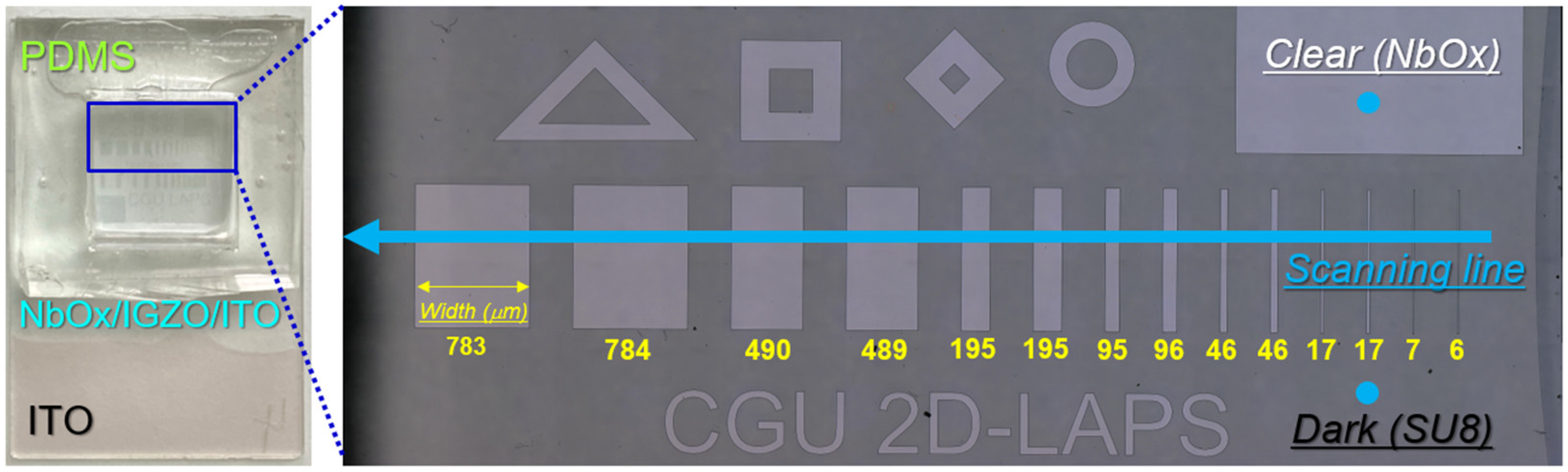
2. Materials and Methods

To investigate the spatial resolution of thin film semiconductors on glass substrates in LAPS, an ITO/glass product (e.g., RLO-I7) provided by Ruilong Inc. (Kaohsiung, Taiwan) was selected to deposit IGZO after surface cleaning with acetone, methanol and deionized (DI) water. Before IGZO deposition by radio frequency (rf) sputtering, vacuum tape was used to protect the electrode contact area. An IGZO target with a purity of 99.9% and a specific atomic ratio (e.g., In:Ga:Zn:O = 1:1:1:4) was purchased (2TIGZO433BSE, Summit-Tech resource corp., Hsinchu, Taiwan). The process pressure was controlled at 8 mTorr with a steady gas mixture (e.g., flow rates of Ar and O2 were 24 and 1 sccm) by 2 mass flow controllers. The rf power was set as 100 W, and the substrate temperature was heated to 250 °C for IGZO deposition with a thickness of 300 nm by the time model controls obtained in from previous experience with studying the deposition rate under the same conditions. [36,37,44] Due to the consideration of a high photocurrent and acceptable process time, the thickness of IGZO layer was decided [44]. The calculated penetration depth of this fabricated IGZO layer on ITO glass under illumination with wavelength of 405 nm could be approximately 3.4 μm based on the optical absorption spectrum from the ultraviolet/visible spectrophotometer (UV-vis) and Tauc method, as shown in Figure S1 [45]. After IGZO deposition, a 35 nm-thick NbOx layer functions as the sensing membrane and is controlled by the time mode, which was fabricated by rf sputtering with a Nb target with a purity of 99.9% in the position of the second gun, fixed Ar and O2 gas flow rates (e.g., 20 and 5 sccm), a pressure of 8 mTorr and an rf power of 200 W. Due to the fact that the extra thermal budget may impact on IGZO and ITO/glass, no substrate heating of the sputtering process and following post-anneal treatment can be performed to this NbOx layer for a better sensing performance. Therefore, the thickness of the NbOx layer is not suggested to be further decrease for the stability requirement. After the whole deposition, the vacuum tape was removed with a wet clean of acetone, methanol and deionized (DI) water to have the exposed ITO layer to collect the photocurrent of IGZO LAPS. To investigate the static 2D chemical images and spatial resolution, in addition to obtaining specific patterns, a photomask with different dimensions, shapes and characters was manufactured on the NbOx surface by a photolithography process using an SU-8 2005 photosensitive epoxy purchased from Kayaku Advanced Materials Inc. (Westborough, MA, USA). A container with polydimethylsiloxane (PDMS) formed by the self-designed mold with a sensing area of 1 × 1 cm2 was attached to the NbOx layer; this setting can be used as the volume for electrolytes and a standard reference electrode for the sensing characteristics measurement [18,36,37]. A picture of this fabricated IGZO LAPS with patterns defined by the SU8–2005 layer with a thickness of approximately 5 μm (e.g., checked by SEM image and not shown here) is shown in Figure 1.
To explore the fabricated IGZO LAPS with pH-sensing characteristics, including the sensitivity and spatial resolution of 2D imaging measurements, an instrument setup with 3 key parts, including input signal generation, output signal processing, and scanning control for data virtualization, was established [36]. The sensing environment was constructed in the container on the IGZO LAPS with an immersed standard Ag/AgCl reference electrode (e.g., Fisherbrand accumet) provided by Fisher Scientific Inc. (Santa Clara, CA, USA) and the standard pH buffer solution purchased from Merck Inc. (Darmstadt, Germany). In the input signal generation part, the data acquisition (DAQ) card was used to provide a gate bias voltage with a sweeping DC mode (e.g., −1.4 to 0.5 V with a step voltage of 0.05 V) between the connections of the reference electrode and the exposed ITO layer. For alternating current (AC)-modulated illumination from the glass side, functioning as the major input signal of IGZO LAPS, different electrical input signals, including the settings of the frequency and trigger current, were supplied to a commercial 405 nm laser (e.g., DL405T/200) purchased from Civil Laser Inc. (Zheijang, China) by the adjustments of a function generator (33500B, Keysight, Trueform Series, Loveland, CO, USA). To check the spatial resolution of static 2D chemical images, the dimensions of the laser spot were controlled by the lens and focused to a minimum size of 12.3 × 12.4 μm, as shown in Figure S2. For output signal processing, a preamplifier (Model SR570, Stanford Research Systems, Sunnyvale, CA, USA) was used to transfer the photocurrent generated by AC modulated illumination by its impedance gain with frequency filtering to be transmitted to the DAQ card to record in the LabVIEW program [36]. For scanning control in the data-virtualization process, the LabVIEW program was used to control an X-Y stage (e.g., SHOT-702) provided by Sigmakoki Inc. (Tokyo, Japan) for the movements of a customized stage fixed with IGZO LAPS, which has the ability to adjust the direction, total length, step distance, and a fixed time period for a predefined and automatic scanning procedure. The coordinates of each pixel were collected and combined with the measured photocurrent for the complete scanning procedure. Therefore, the 2D image can also be easily illustrated by the assistance of the LabVIEW program. For less light and noise interference from the environment, the IGZO LAPS sample, X-Y stage and laser were all shielded in a stainless dark box. Detailed information on this LAPS measurement setup can be found in a previous report [36]. A constant-voltage mode was applied to IGZO LAPS to collect the relative photocurrent of each pixel for linear scanning and 2D imaging [17,32,36].

3. Results and Discussion

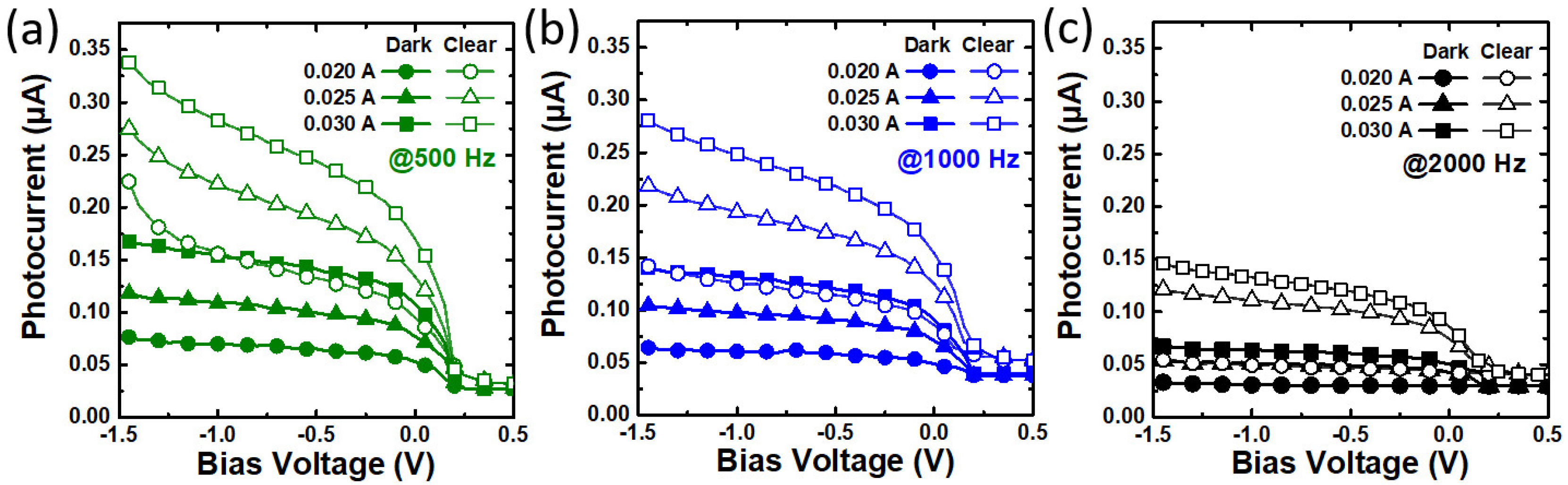
3.1. Basic Characterization of Photoresponse

The IGZO LAPS samples were fabricated with clear and dark zones of different dimensions defined by SU8–2005 photosensitive epoxy and a standard photolithography process, as shown in Figure 1. Following the definition of mask design, clear zones represent the area of the bare NbOx layer on the IGZO layer, and dark zones represent an SU8–2005 layer on the NbOx/IGZO layer. Thus, it was expected that the photocurrents of clear zones would be higher than those of dark zones due to the thick SU8–2005 layer (e.g., 5 μm) functioning as the encapsulation between the sensing membrane and electrolyte. As shown in Figure 1, the locations of the representative clear and dark zones for the standard characteristic measurement are illustrated. Since the objective of this study is to investigate the spatial resolution of the sample patterns, the ability to distinctly identify the boundaries between clear and dark zones is fundamental to be investigated and improved. The photocurrent of the dark zone, referred to as the background noise (N), and the photocurrent of the light zone, referred to as the actual desired signal (S), are studied in detail. On the basis of common parameters, including material, doping, thickness of semiconductor layer and wavelength of light source published in conventional studies, the improvement of spatial resolution is further studied upon the optimization of the operating conditions of the photoillumination process in this study. The two selected parameters are the frequency of the AC modulated input signal and the trigger current applied to the laser source, which together induce different illumination intensities and photocurrents of the LAPS. Additionally, to accurately distinguish zone boundaries, the basic photoresponse of the IGZO LAPS, including a photocurrent versus bias voltage (PC-V) characteristic curve and the signal-to-noise ratio (SNR), was studied. The SNR was collected by the calculation of photocurrent obtained at the clear zones and the dark zones separately by the measured PC-V curve at −1.4 V. First, the PC-V curves were measured in a pH 7 buffer solution by fixing the AC modulation frequency at 500 Hz and varying the trigger current of the laser in the clear and dark zones, as shown in Figure 2a. Next, Figure 2b,c shows the results with the frequency modified to 1000 and 2000 Hz for the same setting of trigger currents, respectively. For a fair parametric analysis, other parameters were kept constant, such as the same pH 7 buffer solution, the same reference electrode, and the sinusoidal laser input having the same following voltage parameters (e.g., peak-to-peak voltage, Vpp = 4 V and direct current voltage, VDC = 2 V). In the clear zone, the behavior of an n-type semiconductor was found to have a high photocurrent in the negative bias region as LAPS operated in inversion mode. The photocurrent decreased as the bias voltage increased because the depletion width decreases from the less revised bias until operation changed to the pure accumulation mode. In the meantime, with the lower trigger current of the laser, the lower intensity of photons supplied the IGZO layer, a few electron-hole pair generations and followed a lower photocurrent. In the dark zone, the photocurrent in the inversion layer was significantly lower than that in the clear zone, matching expectations since the thick encapsulation layer fabricated by the SU8–2005 layer induced a very weak depletion and follows a relatively low photocurrent under the same illumination. In addition, the photocurrent in the accumulation region of the clear and dark zones matched well, which can be considered the same level of background noise in the LAPS measurement. The low-level noise could result from the photons passing through IGZO and then scattering to other IGZO regions by reflection by the reference electrode due to more than 70% transmittance of the IGZO layer, as shown in ultraviolet/visible spectrophotometer (UV-Vis) results reported in previous literature [36]. In addition, the pH-sensing performance and calculated pH sensitivity of the fabricated IGZO LAPS is displayed in Figure S3a,b, and these results were obtained by measuring pH-dependent PC-V curves. The performance is in agreement with the typical behavior reported in the literature [36].

3.2. Correlation of Photocurrent and Signal-to-Noise Ratio

Having a low induced photocurrent and less lateral diffusion is beneficial to spatial resolution; therefore, measuring 2D chemical images with low-intensity laser illumination was designed for this objective. First, a higher AC modulation frequency is therefore desired for a lower photocurrent. However, as evident from the PC-V curves in real measurements, the photocurrent decreases with increasing frequency, limiting the feasible frequency range choices. As a result, the maximum frequency for an acceptable photocurrent is obtained at 2000 Hz from the combined effect of the laser source and IGZO LAPS sample. An AC modulation frequency higher than 2000 Hz yields low-level photocurrents that are practically infeasible for improving spatial resolution performance. Similarly, the limits for the feasible set of trigger currents have been decided after extensive experimentation. Based on the minimum acceptable photocurrent obtained by a criterion that can recognize patterns from background noise, the minimum and maximum trigger currents for all three AC modulation frequencies were decided to be 0.020 and 0.030 A, respectively. To further compare the photoresponse, the photocurrent measured at the most negative bias voltage (e.g., −1.4 V), which is the maximum value in these IGZO LAPS samples, was selected to study the effect of different trigger conditions of illumination. As shown in Figure 3a, the photocurrent increased as the trigger current increased and the AC frequency decreased in both the clear and dark zones. The measured photocurrent in the clear zone was always higher than that in the dark zone. The low-level photocurrent in the dark zone, which can be referred to as the background noise level, impacted the spatial resolution in this study. Before discussing the behavior in detail, it should be mentioned that illuminating a LAPS sample leads to two phenomena, including the generation of electron-hole pairs and their time-dependent propagation to generate a photocurrent. At a higher frequency, less time was available for electron-hole pairs to propagate between the on/off state of illumination, and the minimum trigger current thus had to be higher (e.g., a higher laser intensity was needed to generate more electron-hole pairs) to achieve the acceptable photocurrent. Thus, this trend is the initial indicator of a possible tradeoff between lowering the laser intensity and increasing the frequency to approach a better spatial resolution. However, for lower frequencies, there is more time for electron-hole pair generation and propagation, hence there is a leverage for lowering the minimum trigger current (e.g., the laser intensity can be significantly lower to avoid electron-hole pair crowding) to obtain an acceptable photocurrent. The maximum trigger current was set at 0.030 A with the following light intensity of 13 mW, which is the maximum permissible intensity for illumination of the sample while maintaining the surface integrity of the IGZO LAPS. Laser intensities higher than 13 mW begin to damage the SU8–2005 layer due to the excessive heating effect of the absorption of high-power illumination, as shown in Figure S4 in the Supplementary Materials. To obtain a better understanding, the difference in photocurrent between the clear and dark zones by the grouping of frequency and trigger current is redrawn with a bar chart with different color groupings, as shown in Figure 3b. All white bars are presented for the photocurrent of the dark zone in each group. The difference in photocurrent at −1.4 V presented in different colorful bars in the total measured photocurrent of the clear zone minus the photocurrent of the dark zone. It can be clearly seen that the photocurrent in dark zones (e.g., background signal or noise, named as N), the photocurrent in clear zones (e.g., signal, named as S) and the difference in the photocurrent current between dark and clear zones (e.g., signal-noise) always increased or decreased simultaneously no matter the groups of frequency or trigger current, indicating that the optimized condition of a high signal and low noise together cannot be obtained by this illumination setting. To illustrate the difference between the clear and dark zones with regard to the spatial resolution, a new parameter, the signal-to-noise ratio, SNR, is created to check the potential trend by calculating the ratio of photocurrent measured at −1.4 V of the clear zone over the dark zone. As shown in Figure 3c, the SNR at −1.4 V is drawn with all trigger parameters of illumination. To better understand the exact power of illumination, the laser power of each group is also provided, as shown on the Y2-axis of Figure 3c. The intensity increases linearly with the trigger current. For a fixed frequency, the SNR decreases with the trigger current of the laser for the group operated at 500 and 1000 Hz. Only at a frequency of 2000 Hz is a very low SNR found for the group with a trigger current of 0.020 A, which could be due to the smallest intensity and the highest modulated frequency both causing the photocurrent to not be generated and transported smoothly. For a higher SNR, a high laser intensity is not always desired. A new concept presented in this study uses a new parameter, SNR, to discuss the potential impact on the spatial resolution of LAPS for the first time.

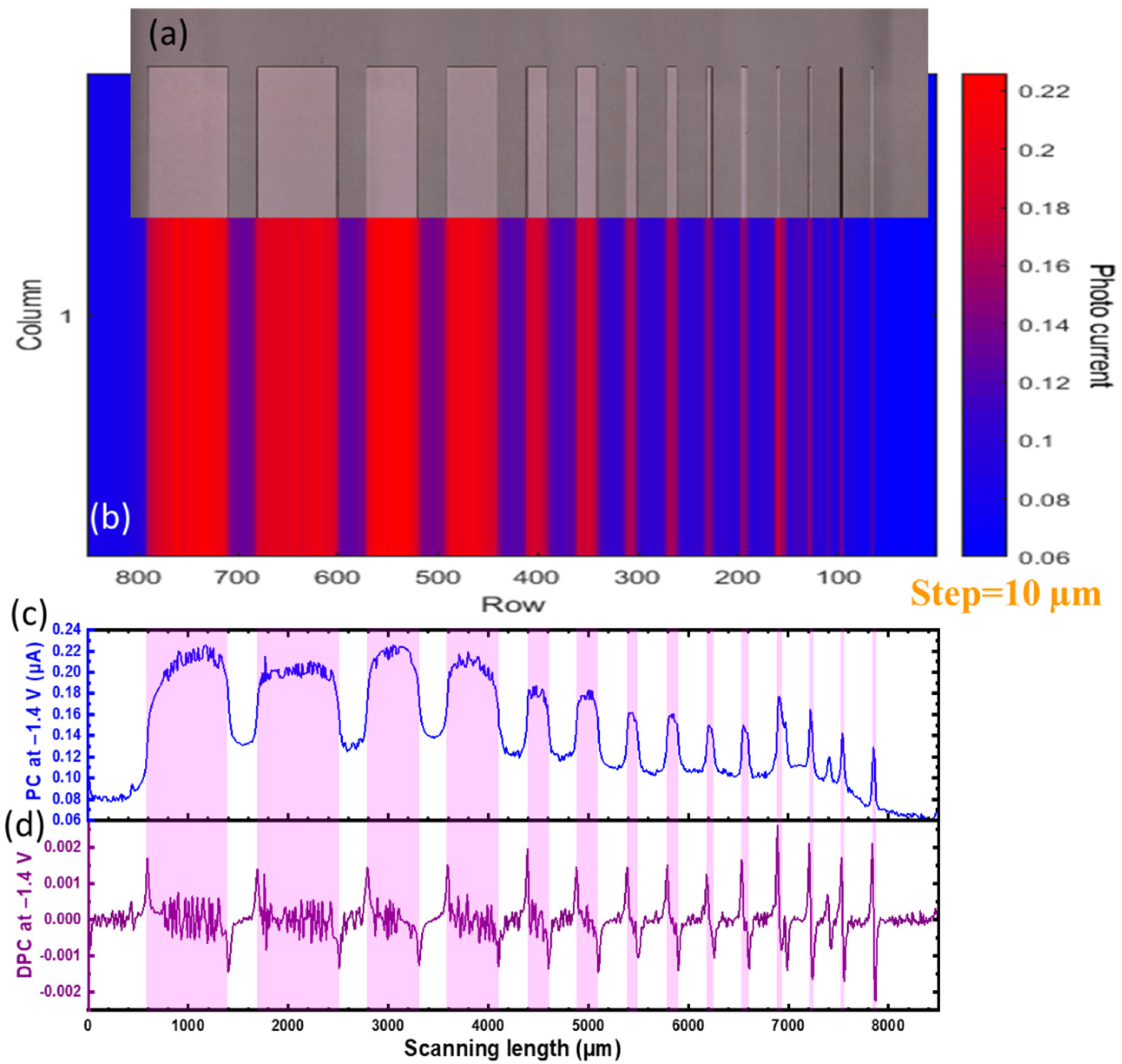
3.3. Conceptualizing and Formulating the Spatial Resolution

By definition, the spatial resolution describes how much detail in a photographic image is visible by the human eye. The ability to “resolve,” or separate, the smallest pixels is one way of describing what we can define as spatial resolution. However, for practical purposes, this idea needs to be quantified into a measurable quantity for scientific analysis. When the LAPS sample with fabricated patterns is subjected to line scanning of illumination, the surfaces with thicker SU8–2005 layers compared to the features/patterns that expose the bare NbOx layer could be used to investigate the difference in the measured signal. These distinct regions show different responses in terms of two distinct levels of photocurrents, as shown in Figure 2a. Therefore, the features/patterns exposing the bare NbOx layer yield a higher photocurrent (e.g., signal) than the rest of the SU8–2005 masked surface (e.g., noise). Then, a scanning process of the laser spot can be performed by the sample movement controlled on a fixed Y-axis and gradual increases in the X coordinate by an X-Y stage scheduled by the LabVIEW program, which is illustrated as marked in the scanning line, as shown in Figure 1. In a line scanning process, the photocurrent was measured with a bias voltage at −1.4 V with a trigger current of 0.025 A at a frequency of 1000 Hz at equispaced points with spacing steps of 10 and 2 μm along a straight line on the LAPS surface were collected to generate photocurrent versus scanning length (PC-SL) plots. The image comparison between the 2D image from the microscope and the measured PC from LAPS is shown in Figure 4a,b, respectively. In a wide range scanning for a fast and rough check, these two patterns are matched well. To perform a detailed verification, the dimensions of clear zones are designed to be 10 to 800 μm in the layout for mask fabrication and to follow the photolithography for the SU8–2005 photosensitive epoxy to verify the limitation of spatial resolution in this study. Corresponding to the width of the fabricated patterns of the LAPS measured by microscopy, as illustrated in Figure 1, the photocurrent with each coordination was collected and plotted in the PC-SL curve, as shown in Figure 4c. This figure depicts the varying crests and troughs of photocurrent detected pixel-by-pixel through all patterned regions of LAPS as the X-Y stage-controlled illumination in the scanning process with a spacing of 10 μm. According to the increasing widths of each line pattern on LAPS, the observed widths of each height in the PC-SL plot increase. The highest photocurrent of the small patterns is lower than that of the large patterns, which can be concluded from the limitation of spot size after diffraction of the LAPS chip being larger than the actual design patterns. At the boundaries between bare NbOx and SU8–2005 masked surfaces, some clear trends of the rise or fall of photocurrents can be clearly observed. This sudden rise-and-fall behavior can be conceptualized clearly in terms of differential photocurrent versus scanning length (DPC-SL) plots, as shown in Figure 4d, following the definition by calculating the full width at half-maximum (FWHM) of the first derivative in the photocurrent response across the edge of the photoresist pattern [17,18,32,36,46]. The locations with a local maximum and local minimum DPC are shown in Figure 4d and can be observed to align along the boundaries of sudden changes in PC, as shown in Figure 4c. This kind of extremum can be considered the cliffs of PC in the boundaries between the NbOx and SU8–2005 layers. Therefore, the distance between each local maximum and its adjacent local minimum in the DPC-SL plot is termed the critical dimension (CD) of each pattern. Using these calculated data, we can finally conceptualize and formulate the quantitative definition of spatial resolution (SR) of the LAPS sample. The superimposition of the DPC-SL plot over the PC-SL plot not only takes into consideration the gradual rise and fall of PC at the boundaries between clear/dark patterns while estimating the critical dimension but also assists in calculating the critical dimension accurately in two ways: (1) eliminating anomalous data in either of these plots for better pattern recognition and (2) correctly identifying the pair of adjacent local maxima and minima corresponding to the rise and fall of PC at the boundaries. The SR ability of LAPS in this study is defined as the absolute difference between the actual width of a particular feature measured by a microscope (e.g., as marked in Figure 1) and the calculation obtained from the LAPS measurement (e.g., by calculating the distance difference from coordination between the maximum and minimum DPC).

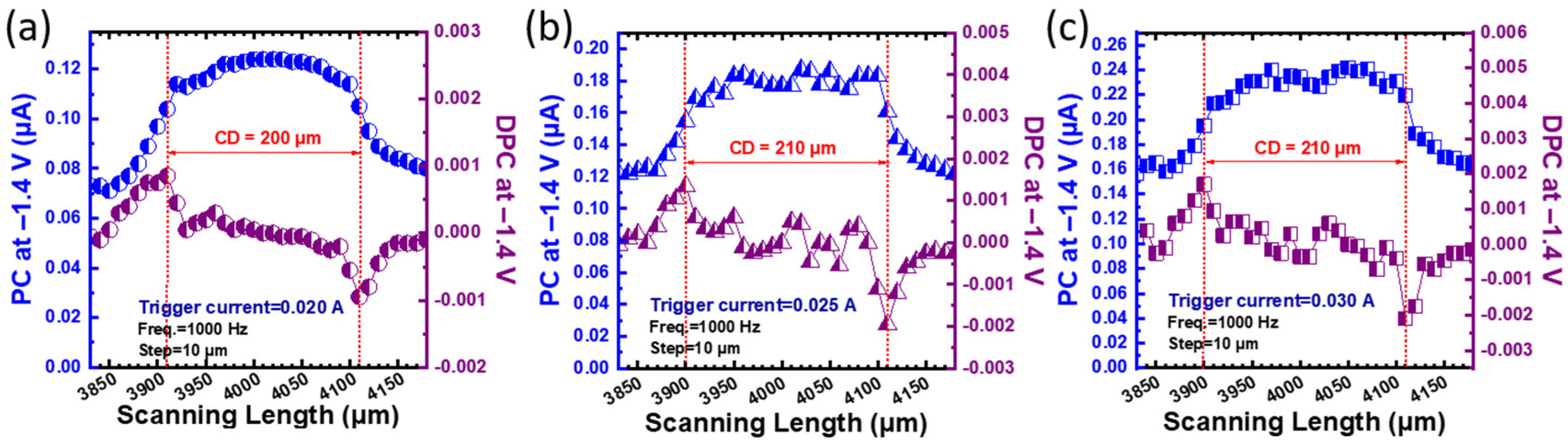
3.4. Spatial Resolution Analysis

A comprehensive experimental investigation on the spatial resolution of the patterned IGZO LAPS sample was performed, following a parametric comparison of the results based upon the two major operating conditions: the frequency and the trigger current of the AC-modulated laser used for illumination. The objective of enhancing the spatial resolution performance of the LAPS essentially means improving the ability of the LAPS to resolve the smallest dimensions of patterns as much as possible. To investigate the small difference between the fabricated SU8–2005 patterns and the measured signals of LAPS, the PC-SL and corresponding DPC-SL curves were redrawn, as shown in Figure 5a, for a trigger current of 0.020 A at an AC frequency of 1000 Hz measured in pH-7 buffer solution. As shown on the Y1-axis of Figure 5a–c, the measured photocurrent versus scanning length (PC-SL) curve for the clear zone with a width of 200 μm can be seen for three trigger currents, including 0.020, 0.025 and 0.030 A, respectively. Line scanning was performed at a spacing step of 10 μm and a bias voltage fixed at −1.4 V for a maximum photocurrent. A clear photocurrent step height can be observed for all three conditions. The baseline and height of the photocurrent both increase with trigger currents. However, this PC-SL curve itself is not fully representative of accurately measuring the critical dimension by a simple cutoff in the behavior because a small photocurrent tail may be generated by the large spot size of illumination and the resulting scattering in a glass substrate. As mentioned in the previous part, the DPC-SL plots shown on the Y2-axis of Figure 5a–c can be used to better compare the spatial resolution. It can be clearly observed that the CD values are 200 and 210 μm at trigger currents of 0.020 A and in other groups, respectively. Therefore, among these three operating conditions under illumination at a frequency of 1000 Hz, the best spatial resolution performance of the 200-μm-wide pattern is obtained for the group with a trigger current of 0.020 A. Some fluctuations may be found in the PC-SL curve, which can be from the natural noise and the instability of the laser. With the combination of PC-SL and the DPC-SL curve, patterns made by the SU8–2005 mask layer can be more efficiently and correctly distinguished. The comparison of patterns with widths of 800 and 50 μm scanned by spacings of 10 and 2 μm with the same illumination setup is also provided, as shown in Figure S5a,b. For a large pattern (e.g., 800 μm), a spacing step of 10 μm is good enough to distinguish the width regardless of the trigger current condition, as shown in Figure S5a. For a small pattern (e.g., 50 μm), a small spacing step of 2 μm is required. However, a critical issue could occur since continuous illumination with high power damaged patterns, which allowed us to select a low trigger current from 0.020 to 0.030 A. The SU8–2005 layer burned after the scanning measurement with a trigger current of 0.035 A is presented in Figure S4. These results prove the earlier hypothesis that spatial resolution performance is not followed simply by increasing the trigger current. Therefore, investigation of the correlation of the signal, noise and SNR with the spatial resolution performance is necessary for the optimization of the spatial resolution of LAPS.
Next, a discussion of the spatial resolution performance comparison considering all the line patterns with different illumination conditions is presented. In the spacing group of 10 μm, patterns with a designed width from 100 to 800 μm (e.g., a total of 8 patterns) are used to test by the consideration of suitable pixel numbers. A spacing of 2 μm is used to check the spatial resolution for patterns with a designed width from 8 to 100 μm (e.g., a total of 8 patterns). For a better understanding of the ability of SR data, a new parameter of delta CD is created by calculating the difference between the CD measured from DPC/PC-SL and from optical microscopy. The median value of each group with different trigger currents and AC frequencies is selected for comparison to avoid fluctuations or noise impacts in the scanning measurements. The median delta CD with all groups scanned with step spacings of 10 and 2 μm versus photocurrent measured at −1.4 V in clear ozone is drawn, as shown in Figure 6a,b. It can be confirmed that a small step spacing results in a small delta CD and follows a better spatial resolution (e.g., delta CD = 0, which essentially means that LAPS perfectly resolves the fabricated line width), which meets scientific expectations. The minimum delta CD values are approximately 4 and 5 μm for step spacings of 2 and 10 μm, respectively. At low frequencies (e.g., 500 and 1000 Hz), a high photocurrent seems to slightly increase delta CD, but the opposite trend is found at a frequency of 2000 Hz. No consistent correlation can be found between the median delta CD and photocurrent measured at −1.4 V in the clear zone for all AC frequencies, indicating that the spatial resolution is not perfectly determined by the photocurrent in the clear zone. In the meantime, the photocurrent in the dark zone also presents a similar behavior to delta CD, as shown in Figure S6. On the contrary, a clear correlation was not found. The trigger current shows a different trend under varying AC frequencies, which could be a complicated effect from the experimental setup contributed by the frequency response of the laser and IGZO optoelectronic transfer mechanism. For a further detailed study, delta CD versus SNR plots for all illumination groups with step spacings of 10 and 2 μm are drawn, as shown in Figure 6c,d. A small optimized region of SNR (e.g., 2.0 to 2.15) seems to be close to the minimum delta CD, both shown for step spacings of 10 and 2 μm. Low SNRs are obtained at high trigger currents at frequencies of 500 and 1000 Hz; these values can be explained by the intensive response of the photocurrent in the dark ozone over the clear zone. This high-noise baseline is harmful to the readiness between the difference between the clear and dark ozone and following a high delta CD. Consequently, a high SNR is generally desired for a low delta CD. In general, laser illumination with a low intensity does not give an acceptable photocurrent signal or an accurate spatial resolution performance due to the potential impact of existing background noise. As shown in Figure 6c,d, the AC frequency at 2000 Hz triggered with 0.025 A has a slightly higher SNR, but the photocurrent level is not sufficiently high to obtain a noise-immunity signal; in particular, extra noise could be generated by the continuous heating and location movements in the scanning measurement. At this moment, the high trigger current may be used to decrease delta CD slightly, which cannot be suggested due to the risk of pattern damage. On the other hand, the higher the SNR is, the lower the delta CD found for AC frequencies at 500 and 1000 Hz is, which can be concluded by the photocurrent remaining at an acceptable level and then the background noise level dominating. If the photocurrent level is too high, the measured delta CD is increased. As clearly seen in Figure 6c,d, the delta CD trending is overall lower in the group illuminating at an AC frequency of 500 Hz than 1000 and 2000 Hz, which means a wide process window and better baseline performance is found. An optimized illumination condition for a driving current of 0.025 A at 500 Hz combined with a spacing of 2 μm in can be used to resolve the pattern width of 10 μm from the pattern width of 6 μm, which is better than the previously reported record of 46 μm from an optical width of 50 μm. To have a smaller spatial resolution (e.g., 1 μm) in the 2D chemical images for cell-relative activity, a miniaturized illumination spot and less photon scattering of IGZO and glass substrate can be suggested for further investigations.

4. Conclusions

In this study, a comprehensive investigation of the photoresponse controlled by various illumination conditions for a 405 nm laser, including trigger current and AC frequency, is first presented to have a smaller spatial resolution of 2D images of IGZO LAPS. The photocurrent (PC) and differential photocurrent (DPC) versus scanning length (SL) are both used to check the resolved critical dimension (CD) from the response of IGZO LAPS. The difference between the resolved CD and optically measured CD (e.g., delta CD) is defined for the spatial resolution study. Experiments at an AC frequency of 500 Hz have an overall smaller delta CD, which can support a precise measurement and better process window. The trigger current level is suggested to be optimized from the tradeoff between the low photocurrent generated by a low power intensity and SU8–2005 mask layer damage induced by a high power intensity. The basic pH-sensing performance of the IGZO layer is comparable under all illumination conditions. This developed methodology provides a possibility for quantitative evaluation with further optimization of the spatial resolution without an extra cost. The signal-to-noise ratio (SNR) has an optimized range of 2.0 to 2.15 for a better resolution for step spacings of both 10 and 2 μm in the scanning procedure to construct static 2D images. Under illumination conditions with a trigger current of 0.025 A and an AC frequency of 500 Hz, the spatial resolution can be reduced to resolve 10 μm from the pattern width of 6 μm. This proposed methodology for the optimization of illumination resulted in a better spatial resolution and can be helpful in 2D chemical imaging-related studies without the extra cost induced by a new instrumentation setup.

Supplementary Materials

The following are available online at https://www.mdpi.com/article/10.3390/chemosensors9110313/s1, Figure S1: Optical absorption spectrum of this fabricated IGZO/ITO/glass sample. Calculated penetration depth is approximately 3.4 μm. Figure S2: The dimensions of the 405 nm laser spot were controlled by the lens and focused to a minimum size of 12.3 × 12.4 μm, which was collected by a commercial beam profiler (NanoScan 2 s, Ophir Photonics, U.S.). Figure S3: (a) Photocurrent versus bias voltage (PC-V) curves measured in various pH buffer solutions and (b) the calculated pH sensitivity and linearity by using the output voltage at the 60% of normalized photocurrent of this fabricated IGZO LAPS sample. Figure S4: The damaged area of the SU8–2005 layer was induced by an excessive heating effect of the absorption of a high-power 405 nm laser illumination with an intensity higher than 13 mW (e.g., trigger current of 0.035 A). Figure S5: PC-SL plots of the patterns with width/spacing ratios of (a) 800/10 μm and (b) 50/2 μm at the same AC frequency of 1000 Hz and trigger currents of 0.020, 0.025, and 0.030 A, respectively. Figure S6: Plot of the median delta CD and photocurrent measured at −1.4 V in the dark zone for all AC frequencies with step spacings of 10 and 2 μm.

Author Contributions

Conceptualization, C.-H.C., Y.-J.L. and C.-M.Y.; methodology, C.-H.C., N.A. and C.-M.Y.; formal analysis, investigation, data curation, and validation, C.-H.C., N.A. and C.-M.Y.; visualization, Y.-J.L. and C.-M.Y.; writing—original draft preparation original manuscript writing, Y.-J.L. and C.-M.Y.; writing—review and editing, Y.-J.L. and C.-M.Y.; supervision, C.-M.Y. All authors have read and agreed to the published version of the manuscript.

Funding

This work was funded by Chang Gung Memorial Hospital, Taiwan under contract numbers CMRPD2I0012, CMRPD2L0171 and the Ministry of Science of Technology of Taiwan under contract numbers 108-2221-E-182-060-MY3, 108-2628-E-182-002-MY3.

Institutional Review Board Statement

Not applicable.

Informed Consent Statement

Not applicable.

Data Availability Statement

The data presented in this study are available on request from the corresponding authors.

Acknowledgments

Neelanjan Akuli and Chia-Ming Yang thanks the student internship program support by International Relations, Indian Institute of Technology Kharagpur and Chang Gung University for opportunities of the science internship at Chang Gung University.

Conflicts of Interest

The authors declare no conflict of interest.

References

  1. Liu, D.; Zhang, H.; Fontana, F.; Hirvonen, J.T.; Santos, H.A. Current developments and applications of microfluidic technology toward clinical translation of nanomedicines. Adv. Drug Deliv. Rev. 2018, 128, 54–83. [Google Scholar] [CrossRef] [PubMed] [Green Version]
  2. Li, L.; Pan, L.; Ma, Z.; Yan, K.; Cheng, W.; Shi, Y.; Yu, G. All Inkjet-Printed Amperometric Multiplexed Biosensors Based on Nanostructured Conductive Hydrogel Electrodes. Nano Lett. 2018, 18, 3322–3327. [Google Scholar] [CrossRef] [PubMed]
  3. Jung, W.; Han, J.; Choi, J.; Ahn, C.H. Point-of-care testing (POCT) diagnostic systems using microfluidic lab-on-a-chip technologies. Microelectron Eng. 2015, 132, 46–57. [Google Scholar] [CrossRef]
  4. Sackmann, E.K.; Fulton, A.L.; Beebe, D.J. The present and future role of microfluidics in biomedical research. Nature 2014, 24, 181–189. [Google Scholar] [CrossRef] [PubMed]
  5. Singh, P. SPR Biosensors: Historical Perspectives and Current Challenges. Sens. Actuators B Chem. 2016, 229, 110–130. [Google Scholar] [CrossRef]
  6. Goud, K.Y.; Moonla, C.; Mishra, R.K.; Yu, C.; Narayan, R.; Litvan, I.; Wang, J. Wearable Electrochemical Microneedle Sensor for Continuous Monitoring of Levodopa: Toward Parkinson Management. ACS Sens. 2019, 4, 2196–2204. [Google Scholar] [CrossRef]
  7. Lowe, B.M.; Sun, K.; Zeimpekis, I.; Skylaris, C.K.; Green, N.G. Field-effect sensors–from pH sensing to biosensing: Sensitivity enhancement using streptavidin–biotin as a model system. Analyst 2017, 142, 4173–4200. [Google Scholar] [CrossRef] [PubMed] [Green Version]
  8. Kaisti, M. Detection principles of biological and chemical FET sensors. Biosens. Bioelectron. 2017, 98, 437–448. [Google Scholar] [CrossRef] [PubMed]
  9. Pullano, S.A.; Critello, C.D.; Mahbub, I.; Tasneem, N.T.; Shamsir, S.; Islam, S.K.; Greco, M.; Fiorillo, A.S. EGFET-Based Sensors for Bioanalytical Applications: A Review. Sensors 2018, 18, 4042. [Google Scholar] [CrossRef] [Green Version]
  10. Sakata, T.; Matsumoto, S.; Nakajim, Y.; Miyahara, Y. Potential Behavior of Biochemically Modified Gold Electrode for Extended-Gate Field-Effect Transistor. Jpn. J. Appl. Phys. 2005, 44, 2860–2863. [Google Scholar] [CrossRef]
  11. Owicki, J.C.; Bousse, L.J.; Hafeman, D.G.; Kirk, G.L.; Olson, J.D.; Wada, H.G.; Parce, J.W. The light-addressable potentiometric sensor: Principles and biological applications. Annu. Rev. Biophys. Biomol. Struct. 1994, 23, 87–113. [Google Scholar] [CrossRef]
  12. Poghossian, A.; Schöning, M.J. Capacitive Field-Effect EIS Chemical Sensors and Biosensors: A Status Report. Sensors 2020, 20, 5639. [Google Scholar] [CrossRef] [PubMed]
  13. Parizi, K.B.; Xu, X.; Pal, A.; Hu, X.; Wong, H.S.P. ISFET pH Sensitivity: Counter-Ions Play a Key Role. Sci. Rep. 2017, 7, 41305. [Google Scholar] [CrossRef] [PubMed] [Green Version]
  14. Lee, C.; Kim, S.K.; Kim, M. Ion-Sensitive Field-Effect Transistor for Biological Sensing. Sensors 2009, 9, 7111–7131. [Google Scholar] [CrossRef] [PubMed]
  15. Huang, X.; Wang, F.; Guo, J.; Yan, M.; Yu, H.; Yeo, K.S. A 64 × 64 1200 fps CMOS Ion-Image Sensor with Suppressed Fixed-Pattern-Noise for Accurate High-throughput DNA Sequencing. In Proceedings of the 2014 Symposium on VLSI Circuits Digest of Technical Papers, Honolulu, HI, USA, 10–13 June 2014. [Google Scholar]
  16. Dantism, S.; Takenaga, S.; Wagner, T.; Wagner, P.; Schöning, M.J. Differential imaging of the metabolism of bacteria and eukaryotic cells based on light-addressable potentiometric sensors. Electrochim. Acta 2017, 246, 234–241. [Google Scholar] [CrossRef]
  17. Yoshinobu, T.; Miyamoto, K.O.; Werner, C.F.; Poghossian, A.; Wagner, T.; Schöning, M.J. Light-Addressable Potentiometric Sensors for Quantitative Spatial Imaging of Chemical Species. Annu. Rev. Anal. Chem. 2017, 10, 225–246. [Google Scholar] [CrossRef]
  18. Yang, C.; Zeng, W.; Chen, C.; Chen, Y.; Chen, T. Spatial resolution and 2D chemical image of light-addressable potentiometric sensor improved by inductively coupled-plasma reactive-ion etching. Sens. Actuators B Chem. 2018, 258, 1295–1301. [Google Scholar] [CrossRef]
  19. Miyamoto, K.; Itabashi, A.; Wagner, T.; Schöning, M.J.; Yoshinobu, T. High-speed chemical imaging inside a microfluidic channel. Sens. Actuators B Chem. 2014, 194, 521–527. [Google Scholar] [CrossRef]
  20. Poghossian, A.; Werner, C.F.; Buniatyan, V.V.; Wagner, T.; Miamoto, K.; Yoshinobu, T.; Schöning, M.J. Towards addressability of light-addressable potentiometric sensors: Shunting effect of non-illuminated region and cross-talk. Sens. Actuators B Chem. 2017, 244, 1071–1079. [Google Scholar] [CrossRef]
  21. Ipatov, A.; Zinoviev, K.; Abramova, N.; Bratov, A. Light addressable potentiometric sensor array: A new approach for light beam positioning. Procedia Eng. 2010, 5, 625–628. [Google Scholar] [CrossRef] [Green Version]
  22. Yang, C.; Chiang, T.; Yeh, Y.; Das, A.; Lin, Y.; Chen, T. Sensing and pH-imaging properties of niobium oxide prepared byrapid thermal annealing for electrolyte–insulator–semiconductorstructure and light-addressable potentiometric sensor. Sens. Actuators B Chem. 2015, 207, 858–864. [Google Scholar] [CrossRef]
  23. Özsoylu, D.; Kizildag, S.; Schöning, M.J.; Wagner, T. Differential chemical imaging of extracellular acidification within microfluidic channels using a plasma-functionalized light-addressable potentiometric sensor (LAPS). Phys. Med. 2020, 10, 100030. [Google Scholar] [CrossRef]
  24. Liang, T.; Gu, C.; Gan, Y.; Wu, Q.; He, C.; Tu, J.; Pan, Y.; Qiu, Y.; Kong, L.; Wan, H.; et al. Microfluidic chip system integrated with light addressable potentiometric sensor (LAPS) for real-time extracellular acidification detection. Sens. Actuators B Chem. 2019, 301, 127004. [Google Scholar] [CrossRef]
  25. Hu, N.; Wu, C.; da, H.; Wang, T.; Liu, Q.; Wang, P. A novel microphysiometer based on high sensitivity LAPS and microfluidic system for cellular metabolism study and rapid drug screening. Biosens. Bioelectron. 2013, 40, 167–173. [Google Scholar] [CrossRef] [PubMed]
  26. Dantism, S.; Röhlen, D.; Dahmen, M.; Wagner, T.; Wagner, P.; Schöning, M.J. LAPS-based monitoring of metabolic responses of bacterial cultures in a paper fermentation broth. Sens. Actuators B Chem. 2020, 320, 128232. [Google Scholar] [CrossRef]
  27. Guo, Y.; Miyamoto, K.; Wagner, T.; Schöning, M.J.; Yoshinobu, T. Device simulation of the light-addressable potentiometric sensor for the investigation of the spatial resolution. Sens. Actuators B Chem. 2014, 204, 659–665. [Google Scholar] [CrossRef]
  28. Guo, Y.; Miyamoto, K.; Wagner, T.; Schöning, M.J.; Yoshinobu, T. Theoretical study and simulation of light-addressable potentiometric sensors. Phys. Status Solidi 2014, 211, 1467–1472. [Google Scholar] [CrossRef]
  29. Zhang, Q. Theoretical analysis and design of submicron-LAPS. Sens. Actuators B Chem. 2005, 105, 304–311. [Google Scholar] [CrossRef]
  30. Hu, N.; da, H.; Wu, C.; Zhou, J.; Kirsanov, D.; Legin, A.; Wan, P.g. A LAPS array with low cross-talk for non-invasive measurement of cellular metabolism. Sens. Actuator A Phys. 2012, 187, 50–56. [Google Scholar] [CrossRef]
  31. Chen, D.; Liu, S.; Yin, S.; Liang, J. Light-addressable potentiometric sensor with the micro blind holes substrate. IET Sci. Meas. Technol. 2017, 11, 57–62. [Google Scholar] [CrossRef]
  32. Yang, C.; Zeng, W.; Chen, Y.; Chen, T. Surface Modification for High Photocurrent and pH Sensitivity in a Silicon-Based Light-Addressable Potentiometric Sensor. IEEE Sens. J. 2018, 18, 2253–2259. [Google Scholar] [CrossRef]
  33. Chen, L.; Zhou, Y.; Jiang, S.; Kunze, J.; Schmuki, P.; Krause, S. High resolution LAPS and SPIM. Electrochem. Commun. 2010, 2, 758–760. [Google Scholar] [CrossRef]
  34. Ito, Y. High-spatial resolution LAPS. Sens. Actuators B Chem. 1998, 52, 107–111. [Google Scholar] [CrossRef]
  35. Yang, C.; Liao, Y.; Chen, C.; Chen, T.; Lai, C.; Pijanowska, D.G. P-I-N amorphous silicon for thin-film light-addressable potentiometric sensors. Sens. Actuators B Chem. 2016, 236, 1005–1010. [Google Scholar] [CrossRef]
  36. Yang, C.; Chen, C.; Akuli, N.; Yen, T.; Lai, C. A revised manuscript submitted to sensors and actuators B: Chemical illumination modification from an LED to a laser to improve the spatial resolution of IGZO thin film light-addressable potentiometric sensors in pH detections. Sens. Actuators B Chem. 2021, 329, 128953. [Google Scholar] [CrossRef]
  37. Yang, C.; Chen, C.; Chang, L.; Lai, C. IGZO Thin-Film Light-Addressable Potentiometric Sensor. IEEE Electron Device Lett. 2016, 37, 1481–1484. [Google Scholar] [CrossRef]
  38. Kamiya, T.; Nomura, K.; Hoson, H.o. Present status of amorphous In–Ga–Zn–O thin-film transistors. Sci. Technol. Adv. Mater. 2010, 11, 44305. [Google Scholar] [CrossRef] [PubMed]
  39. Das, A.; Das, A.; Chang, L.B.; Lai, C.S.; Lin, R.M.; Chu, F.C.; Lin, Y.H.; Chow, L.; Jeng, M.J. GaN Thin Film Based Light Addressable Potentiometric Sensor for pH Sensing Application. Appl. Phys. Express 2013, 6, 36601. [Google Scholar] [CrossRef]
  40. Miyamoto, K.O.; Seki, K.; Suto, T.; Werner, C.F.; Wagner, T.; Schöning, M.J.; Yoshinobu, T. Improved spatial resolution of the chemical imaging sensor with a hybrid illumination that suppresses lateral diffusion of photocarriers. Sens. Actuators B Chem. 2018, 273, 1328–1333. [Google Scholar] [CrossRef]
  41. Tan, J.; Liu, S.; Luo, J.; Li, H. Well-ordered polystyrene colloidal spheres for light addressable potentiometric sensor. Thin Solid Films 2020, 716, 138417. [Google Scholar] [CrossRef]
  42. Chen, C.; Yang, C.; Chang, L.; Lai, C. Thickness effect of IGZO layer in light-addressable potentiometric sensor. In Proceedings of the 2016 23rd International Workshop on Active-Matrix Flatpanel Displays and Devices (AM-FPD), Kyoto, Japan, 6–8 July 2016. [Google Scholar]
  43. Fung, T.Z. Amorphous In-Ga-Zn-O Thin Film Transistor for Future Optoelectronics. Ph.D. Dissertation, University of Michigan, Ann Arbor, MI, USA, 2010; pp. 62–63. [Google Scholar]
  44. Das, A.; Chen, T.; Yang, C.; Lai, C. A high-speed, flexible-scanning chemical imaging system using a light-addressable potentiometric sensor integrated with an analog micromirror. Sens. Actuators B Chem. 2014, 198, 225–232. [Google Scholar] [CrossRef]
  45. Das, A.; Yang, C.; Chen, T.; Lai, C. Analog micromirror-LAPS for chemical imaging and zoom-in application. Vacuum 2015, 118, 161–166. [Google Scholar] [CrossRef]
  46. Zhang, D.; Wu, F.; Kraus, S.E. LAPS and SPIM Imaging Using ITO-Coated Glass as the Substrate Material. Anal. Chem. 2017, 89, 8129–8133. [Google Scholar] [CrossRef] [PubMed]
Figure 1. The fabricated IGZO LAPS sample with SU8 photosensitive epoxy and PDMS encapsulation on the NbOx surface. The ITO layer is exposed as the backside contact of IGZO LAPS. The clear and dark zones for PC-V curve measurement and the scanning line of the spatial resolution check for the patterns with different widths are all marked in the picture captured by an optical microscope.
Chemosensors 09 00313 g001
Figure 2. PC-V curves of IGZO LAPS with clear and dark zones defined by the SU8–2005 layer measured in a pH 7 standard buffer solution with various trigger currents, including 0.020, 0.025 and 0.030 A and 405 nm laser modulated with AC frequencies of (a) 500, (b) 1000 and (c) 2000 Hz.
Chemosensors 09 00313 g002
Figure 3. Photocurrent at −1.4 V for the dark and clear zones under different trigger currents and AC frequencies: (a) scatter plot with connection line and (b) bar chart with different colors. All values of the dark zone are marked in white. (c) The signal-to-noise ratio and the intensity of laser illumination of different trigger currents and AC frequencies.
Chemosensors 09 00313 g003
Figure 4. (a) Image from an optical microscope, (b) image generated from the LabVIEW interface by collecting photocurrents and coordinates, (c) photocurrent and (d) differential photocurrent versus its Y coordinates with a DC bias at −1.4 V and illumination with a trigger current of 0.025 A and AC frequency at 1000 Hz in line scanning with a step spacing of 10 μm controlled by an X-Y stage.
Chemosensors 09 00313 g004
Figure 5. Photocurrent (PC) and differential photocurrent (DPC) versus scanning length curve for IGZO LAPS with a 200 μm-wide clear zone measured in pH 7 buffer solution at AC frequency at 1000 Hz with trigger currents of (a) 0.020, (b) 0.025 and (c) 0.030 A.
Chemosensors 09 00313 g005
Figure 6. The photocurrent measured at −1.4 V in clear ozone versus the median value of delta CD for step spacings of (a) 10 and (b) 2 μm. The SNR at −1.4 V in the clear ozone versus the median value of delta CD for step spacings of (c) 10 and (d) 2 μm. A clear optimized operating region for a small delta CD can be found for SNRs from 2.0 to 2.15.
Chemosensors 09 00313 g006
Publisher’s Note: MDPI stays neutral with regard to jurisdictional claims in published maps and institutional affiliations.

