Article

Tungsten-Based Cost-Effective Gas Sensors for H2S Detection

by
Didier Fasquelle
1,*,
Nathalie Verbrugghe
1 and
Stéphanie Députier
2
1
Unité de Dynamique et Structure des Matériaux Moléculaires (UDSMM), Université du Littoral Côte d’Opale (ULCO), BP699, 62228 Calais, France
2
Université de Rennes, CNRS, ISCR_UMR 6226, F-35000 Rennes, France
*
Author to whom correspondence should be addressed.
Chemosensors 2021, 9(11), 295; https://doi.org/10.3390/chemosensors9110295
Submission received: 9 September 2021 / Revised: 7 October 2021 / Accepted: 14 October 2021 / Published: 20 October 2021
(This article belongs to the Special Issue Anisotropic Nanomaterials for Sensing Applications)

Abstract

:
Tungsten trioxide thin films were deposited on silicon substrates by non-reactive RF sputtering from a WO3 target at room temperature. The WO3 films were post-annealed at two different temperatures, 400 °C and 500 °C. The morphological and microstructural properties of these films were analyzed by using atomic force microscopy and X-ray diffraction. X-ray diffraction patterns only show WO3 oxide phases. The AFM images show different morphologies with smaller grains for the film annealed at 400 °C. WO3 sensing films and W heating elements were embedded in commercial cases for the fabrication of cost-effective gas sensors. The sensitivity and dynamic response of the sensors were analyzed under various concentrations of H2S, from 20 to 100 ppm, at SIMTRONICS SAS (3M Company, Saint Paul, MN, USA). A good sensitivity G/G0 of about 6.6 under H2S 100 ppm was obtained with the best sensor. An interesting dynamic response was observed in particular with a short response time. Additionally, the evolution of the sensitivity was studied, and a conduction model was proposed for explaining the conduction mechanism under H2S exposition.

1. Introduction

The detection of hazardous gases such as CO, H2S, and NO2 is commonly done by semiconductor gas sensors. Indeed, this sensor family is cost-effective, and their sensitivity can be very good [1,2]. This kind of gas sensor is composed of two elements: the sensing layer and the heater. This heater, which can operate at high temperature, is used to heat the sensing layer for tuning the peak of sensitivity. The operating temperature of the heater can range from 200 to 500 °C. The performance of gas sensors is defined by three main characteristics: sensitivity, selectivity, and stability, which is usually called the 3-S rule. Sensitivity is defined by a change of the measured signal, which is function of the sensor resistance variation per analyte concentration unit. Selectivity defines if a sensor can respond selectively to a group of analytes or even specifically to a single analyte. Stability is the ability of a sensor to provide reproducible results in a considered period of time. That means that stability is defined by considering the global behavior, i.e., sensitivity, selectivity, response and recovery times, and cycling. Nevertheless, for applications in industry, the parameter of first importance is the sensor cost. It should be as low as possible, i.e., lower than 5 US dollars per unit. This point justifies the existence of semiconducting gas sensors, even if they are less sensible than optical sensors, even if their selectivity is not very good, and even if they need more electric power, in particular for the heater. Nevertheless, the electric consumption is expected to be lower than 100 mW.
For semiconductor oxides, the gas detection is related to the resistance variation of the sensing layer. This variation results from reactions between the sensing layer and the ambient gas molecules [3,4]. In view to enhance the adsorption/desorption process of the gas molecules, here mainly located at the sensing film surface, the operating temperature of the sensor must be adjusted. Platinum is widely used for manufacturing the heating element. Indeed, Pt displays interesting characteristics: good thermal properties, high resistance to corrosion, and high operating temperature. However, its cost is particularly high, which became a limiting factor for applications. Nowadays, tungsten can be used for the fabrication of integrated heaters. In fact, tungsten heaters can operate in a more limited temperature range than Pt, below 500 °C [5]. Here, the heating element has been especially developed to be integrated to commercial housings. Our goal was to develop a cost-effective gas sensor that is only based on tungsten (metal and oxide). In solid-state gas sensors, the sensing layer is commonly made with transition metal oxides such as SnO2, ZnO, TiO2, and WO3 [1,2]. Tungsten trioxide is very promising because WO3 thin films have demonstrated their efficiency in the detection of various gases, such as H2S and NOx [6,7]. A sensor for the detection of hydrogen sulfide is of great interest because H2S, even in small concentrations, is highly poisonous to humans. In this way, our industrial partner has a particular interest in the H2S detection for the protection of workers on oil extraction sites.
The microstructure, electrical properties, and stoichiometry of the WO3 active layer have a strong influence on the sensor characteristics and are driven by the deposition and the annealing conditions. Then, the WO3 resistivity is strongly influenced by its stoichiometric defects [8]. Several methods have been used for the elaboration and deposition of tungsten oxide films: thermal evaporation [9], sol–gel [10], pulsed electro-deposition [11], and radio-frequency sputtering [12,13], among others. RF sputtering is a widely used technique for the deposition of WO3 thin films. Reactive sputtering from a metallic target gives thin films with a good oxygen stoichiometry [12]. In opposition, the non-reactive sputtering can give oxygen-deficient oxide films when they are deposited at low argon pressure from a metal–oxide target [14,15]. Very few data about WO3 thin films deposited by RF non-reactive sputtering from a tungsten oxide target and their utilization in gas-sensing applications can be found in the literature.
Tungsten trioxide can present five distinct crystallographic phases between 0 and 1200 K: monoclinic (ε-WO3), triclinic (δ-WO3), monoclinic (γ-WO3), orthorhombic (β-WO3), and tetragonal (α-WO3) [16,17]. These five structures are close to each other and can all be described as a tridimensional network of WO6 octahedra. In this network, the phase transitions can be correlated to the tilting of the octahedral and/or the displacement of the tungsten atom inside each octahedron. These phase transitions are also strongly affected by impurities and non-stoichiometry. For thin oxide layers, the substrate material and deposition method will have an important effect as well. In most cases, WO3 thin films deposited by the sputtering technique and annealed at temperature higher than 400 °C present a γ-WO3 monoclinic crystalline structure [13,14,15,18].
In the present study, the microstructure, electrical properties, and exposure to H2S of WO3 thin films were investigated. RF non-reactive sputtering was used to deposit thin films on silicon substrates. Then, these films were annealed at two different temperatures, here 400 °C and 500 °C. WO3 sensing elements associated to a tungsten-based heater were embedded in commercial cases for the fabrication of gas sensors. The electrical response and sensitivity of the cost-effective gas sensors were measured at different operating temperatures and under various concentrations of H2S at SIMTRONICS SAS (3M Company). Additionally, an original study is proposed. Indeed, the sensitivity evolution is explained by a model, and the experimental data are fitted by using equations related to this model. Therefore, an innovative and original study of WO3 cost-effective gas sensors is presented, where the sensitivity evolution of thin films exposed to hydrogen sulfide is explained.

2. Materials and Methods

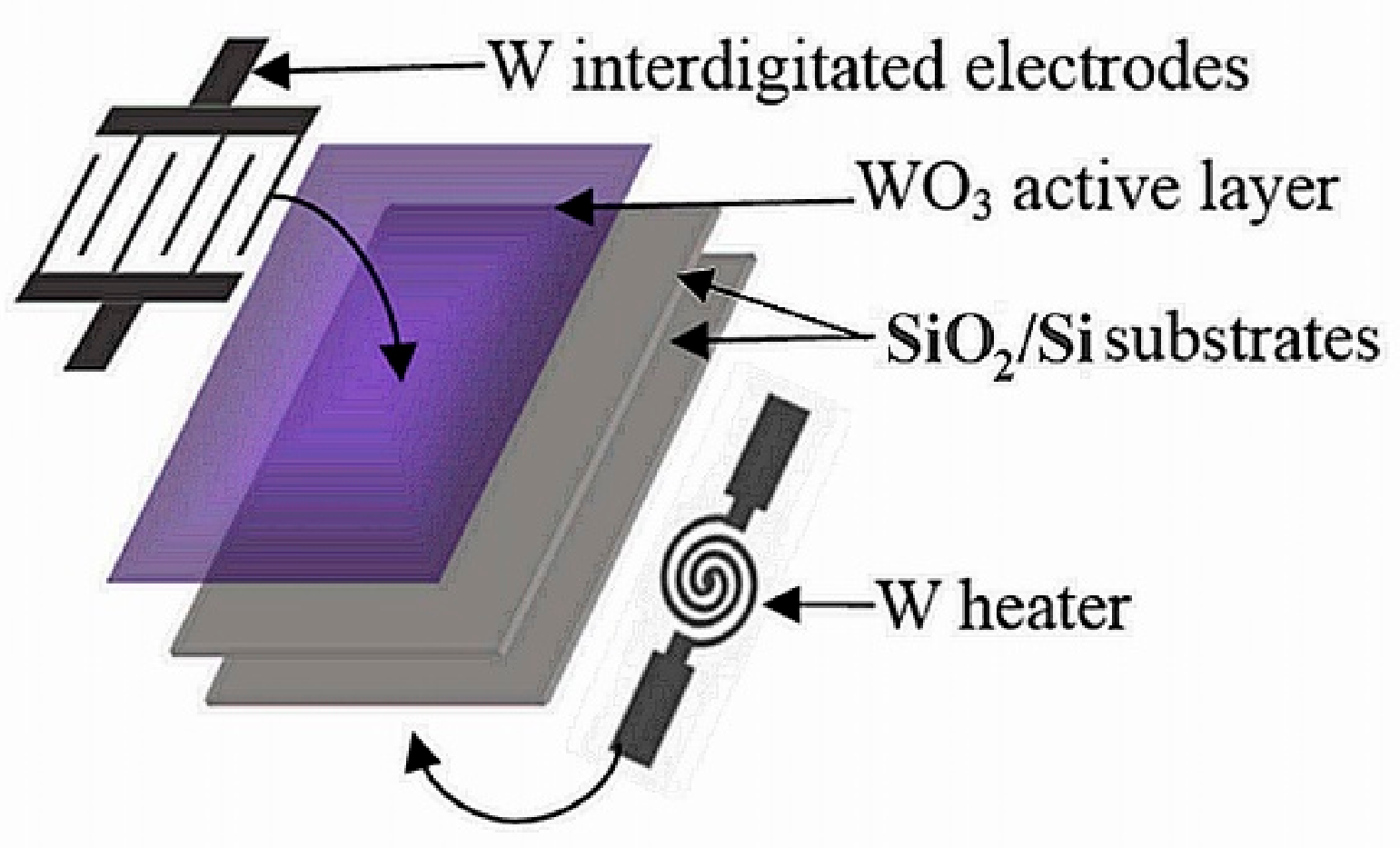
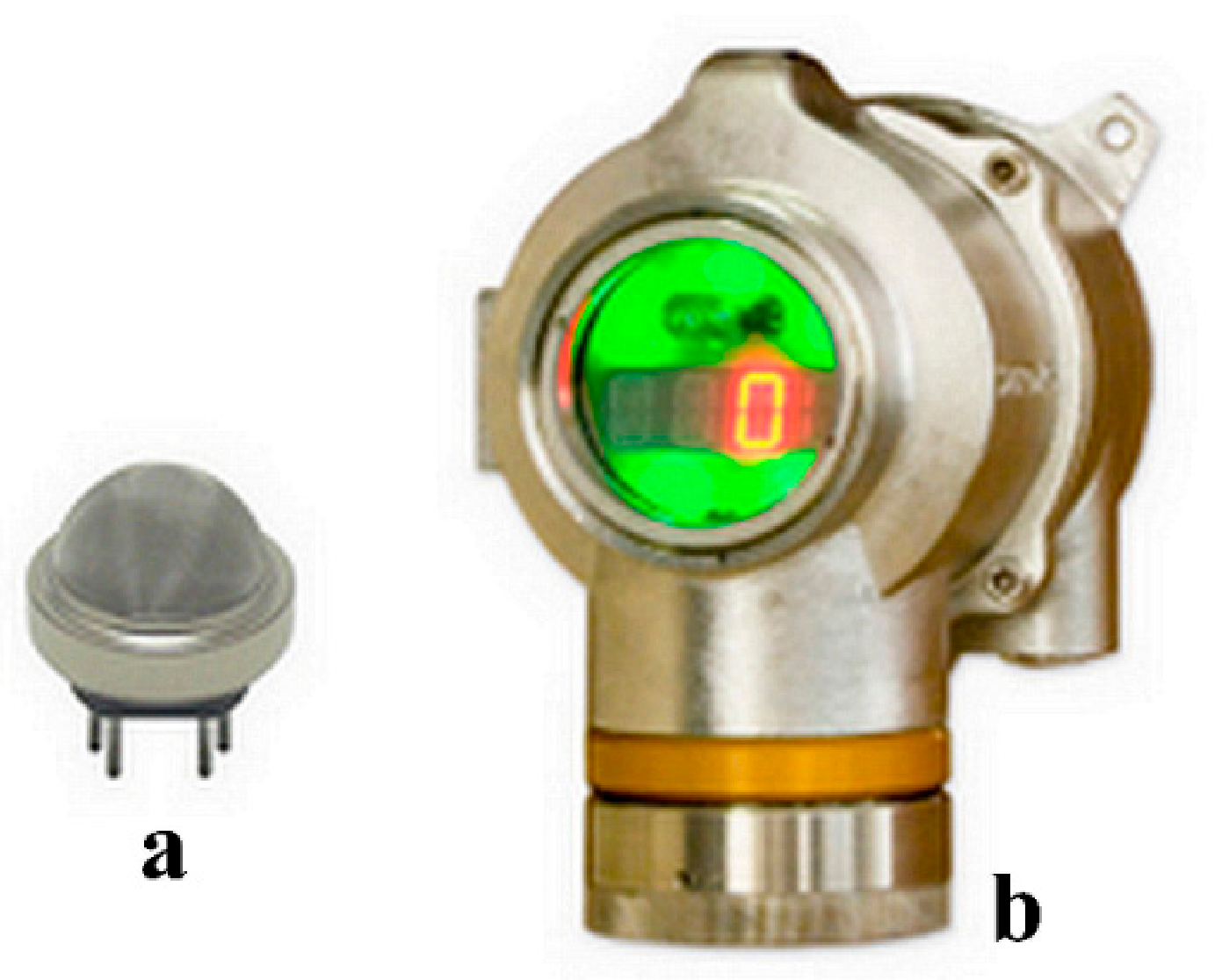
2.1. Sensor Fabrication

2.1.1. Heating Element

An optical lithography technique was used for the elaboration of tungsten double-spiral heaters. Tungsten films were deposited by DC sputtering onto SiO2 (1 µm)/Si (100) N-type substrates. The purity of the tungsten target was 99.95%. The argon pressure was 0.1 Pa. Details about the deposition of tungsten films have already been published [5]. The heater dimensions are 4 mm × 2 mm. The choice of a double-spiral pattern is due to the lower power consumption when compared to other studied structures [5]. In addition, the double spiral has given a better homogeneity of heating and a longer service life.
Commercial PT 100 sensors, stuck on the back of the substrate, were used to measure the heater temperature as a function of the power supply. The electric power supplied to the heater was monitored to keep the sensor at the desired operating temperature. Then, the heater was stuck to the sensing element by using silver ink. The structure of the gas sensor is presented in Figure 1. All heater characteristics are summarized in Table 1.

2.1.2. Sensing Element

Non-reactive RF sputtering was used for the deposition of WO3 thin films. These films were deposited onto SiO2/Si commercial substrates. The purity of the commercial WO3 target (Neyco) was of 99.9%. Pure argon (99.99%) was used as the sputtering gas. The deposition parameters were as follows: a chamber pressure of 1 Pa, RF power of 100 W, substrate not heated. All sputtered films were amorphous, so an annealing step was added after deposition for obtaining crystalline films. The annealing parameters were as follows: 6 h in air, at two different temperatures, 400 °C and 500 °C. To study the influence of the annealing temperature on the sensor response, we have defined 2 annealing temperatures. For the electrical measurements, we have deposited top tungsten interdigitated electrodes by sputtering. An optical lithography technique was used to design these interdigitated electrodes. DC magnetron sputtering was used for the electrode deposition. All characteristics of the sensor parts are presented in Table 1. The sensor made with the WO3 film annealed at 400 °C is noted as sensor-400. The sensor made with the WO3 film annealed at 500 °C is noted sensor-500.

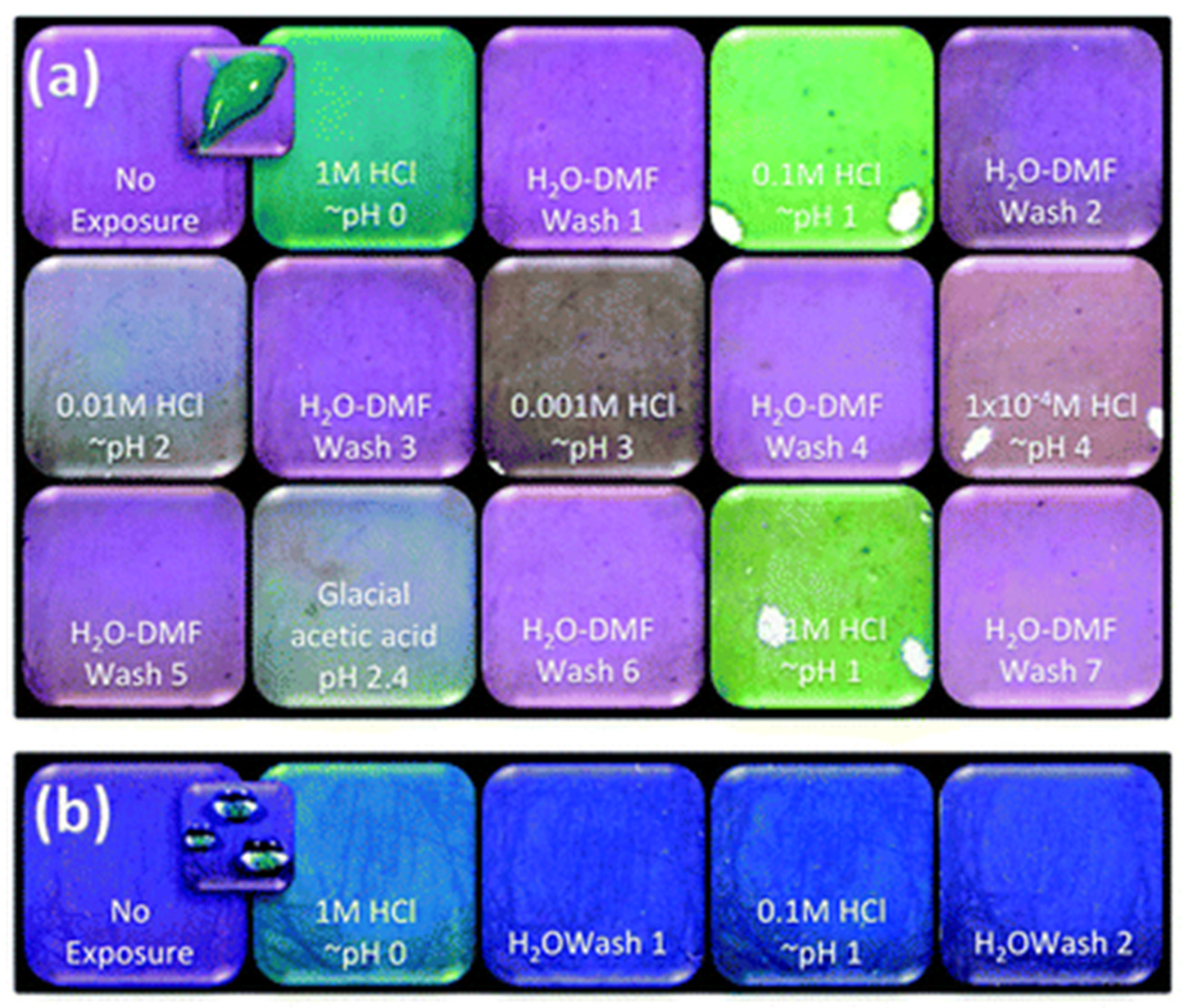
2.2. Physical and Electrical Characterizations

The thicknesses of the tungsten and tungsten trioxide films were determined by observing the cross-section of samples by FESEM (Field-Emission Scanning Electron Microscope JEOL JSM-7100F). Atomic force microscopy was used to study the topography of the thin films, i.e., morphology, grain size, and roughness (Multimode AFM, ex-Veeco Instruments, became a part of Brüker Corp., Billerica, MA, USA). X-ray diffraction (XRD) using a Bruker D8 Advance diffractometer with a monochromatized Cu Kα1 wavelength (λ = 1.54056 Å) in θ-2θ Bragg-Brentano geometry was used to study the crystalline structure of the oxide thin films. Sensing films and heaters were embedded into commercial cases, as shown in Figure 2a. The DG-TT7 Solid-State Gas Detector, from Simtronics SAS, shown in Figure 2b, was used to connect the gas sensors. The DG-TT7 can communicate with a computer by infrared wireless. Configuration and measurements data are transferred and collected by software developed by Simtronics. All experimental measurements were done under different conditions and gas concentrations. Then, all sensing parameters, i.e., sensitivity, response and recovery times, and sensor stability, were computed from experimental data.

3. Results and Discussion

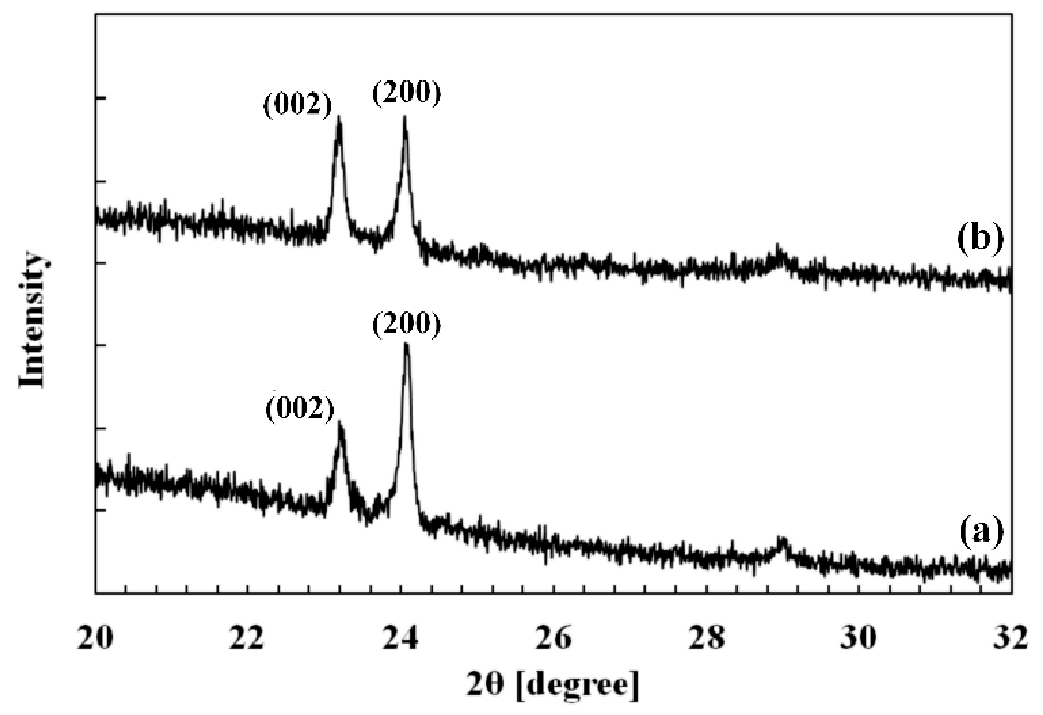
3.1. Crystallographic Structure of WO3 Films

The crystalline structure of thin films was investigated by X-ray diffraction. Figure 3 shows X-ray diffraction patterns of films annealed at 400 °C (pattern (a)) and 500 °C (pattern (b)) for 6 h. The 2θ analysis was initially done from 20° to 75° with a resolution of 0.008° and a step time of 4 s. Both films show two main peaks around 23° and 24°. Some other peaks with an insignificant intensity are located around 29°, 34°, and 42°. So, we have focused on angles ranging from 23° to 32° in Figure 3. The main peaks could correspond to either the triclinic (δ-WO3), monoclinic (γ-WO3), or orthorhombic (β-WO3) structure (JCPDS files: 20-1323, 43-1035, 01-071-0131). No other phase of the W-O system can be associated to these diffraction peaks. It is quite impossible to distinguish which of these WO3 polymorphs is effectively present because these crystalline structures are very close to each other.
The interplanar distances (d) were calculated using Bragg’s law. The crystallite size (Lhkl) normal to the film surface (normal coherence length) was calculated with Scherrer’s formula from the FWHM of each peak. All values are given in Table 2. Taking into account the error margin of the diffractometer, the positions of the diffraction peaks and the related calculated interplanar distances are quite the same for both films. As can be seen in Table 2, the main difference between the crystallite size of the two films is related to the (200) plane.

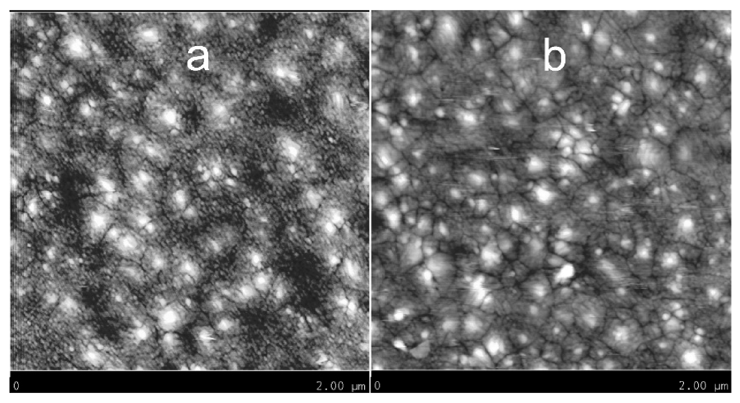
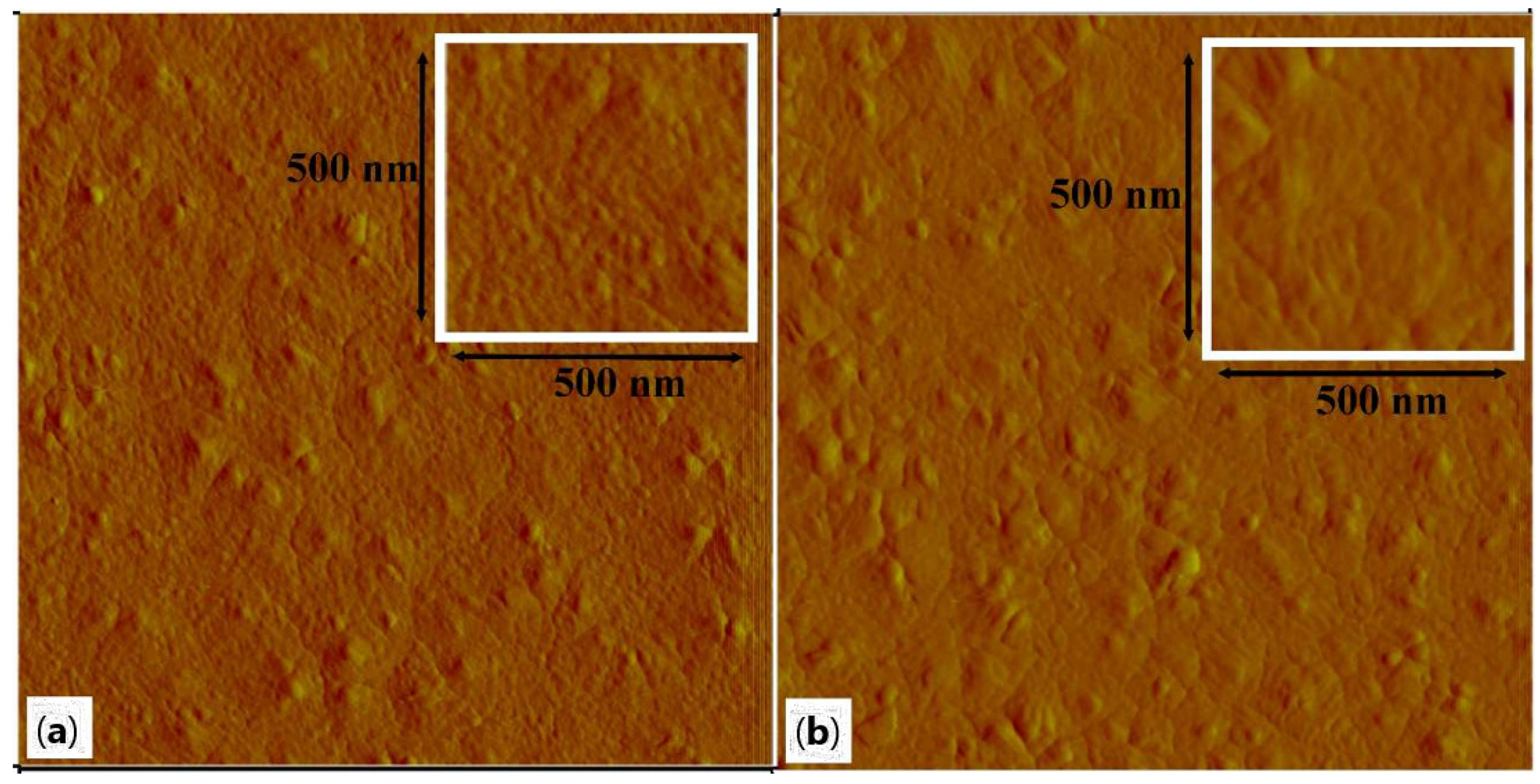
3.2. Surface Morphology of WO3 Films

The surface of WO3 films annealed at 400 °C and 500 °C was observed by AFM to understand how the annealing temperature affects the morphology of the films. Figure 4a,b show the surface microstructure over a 2 µm × 2 µm area. As shown in Figure 4a and its inset, the sample annealed at 400 °C presents a granular surface composed of very small grains, from 14 to 28 nm, and some bigger ones, from 42 to 70 nm. Figure 4b and its inset show the surface of the film annealed at 500 °C. Here, the amount of very small grains has decreased due to the higher annealing temperature. The bigger grains range from 48 to 98 nm. The size of the biggest grains is well correlated to the crystallite sizes given in Table 2 for the two films. The r.m.s. roughness is quite similar for both films, 1.40 nm for the sample annealed at 400 °C and 1.33 nm for the other one. These values of roughness indicate that both films are very smooth. That also suggests the grain growth is very limited in the c-axis when the annealing temperature increases. In fact, the bigger grains have grown in directions parallel to the substrate. So, this particular growth did not significantly affect the roughness of films. To have additional information about the film microstructure, we have applied a numerical treatment to the original AFM images. The treated images are presented in Figure 5. The film annealed at 400 °C is effectively composed of very tiny grains. However, the most important difference can be seen in Figure 5b, where the film annealed at 500 °C reveals bigger grains with well-marked grain boundaries. For both films, the thickness is about 120 nm. The FESEM images used for this measurement by observation of the cross-section are not presented here.

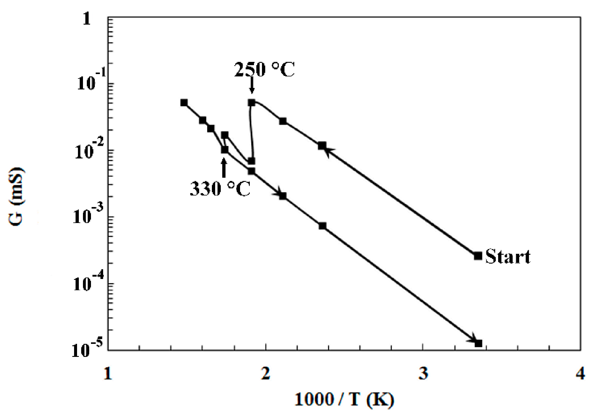
3.3. Electrical Properties

The electrical conductance of the sensors was measured as a function of the operating temperature, here ranging from 25 to 400 °C. The conductance has shown a quite similar behavior for both sensors. So, Figure 6 only presents the conductance evolution of sensor-400 as a function of reciprocal temperature. From room temperature to 250 °C, the electrical conductance G increases when the operating temperature increases. At 250 °C, the conductance value abruptly decreases, and its behavior stays quite unstable until 330 °C. Then, from 330 to 400 °C, the sensor re-finds a classical n-type semiconductor behavior with an increase in its conductance. By cooling the sensor from 400 °C to room temperature, the conductance presents a quite linear evolution. However, the abrupt variation around 250 °C is no longer observed. It is worthy to add that this sensor behavior was reproducible. In fact, additional heating–cooling cycles were operated, and no change in behavior and conductance value was observed.
The observed behavior of the electrical conductance of the sensors could be attributed to the presence of an orthorhombic phase in the WO3 films. Indeed, the orthorhombic phase appears around 320 °C in bulk WO3 [16,20,21]. So, we can suppose that the monoclinic to orthorhombic phase transition occurs from 250 to 330 °C in these WO3 thin films. Above 330 °C, the phase transition ends, and the sensors present a stable behavior without any hectic variation of the conductance. So, the temperature range from 250 to 330 °C has been avoided for gas measurements in this study, because it is therefore impossible to accurately calculate the sensitivity when the sensor shows such abrupt variation of its conductance. In addition, a good repeatability of the conductance measurements cannot be obtained in such conditions.

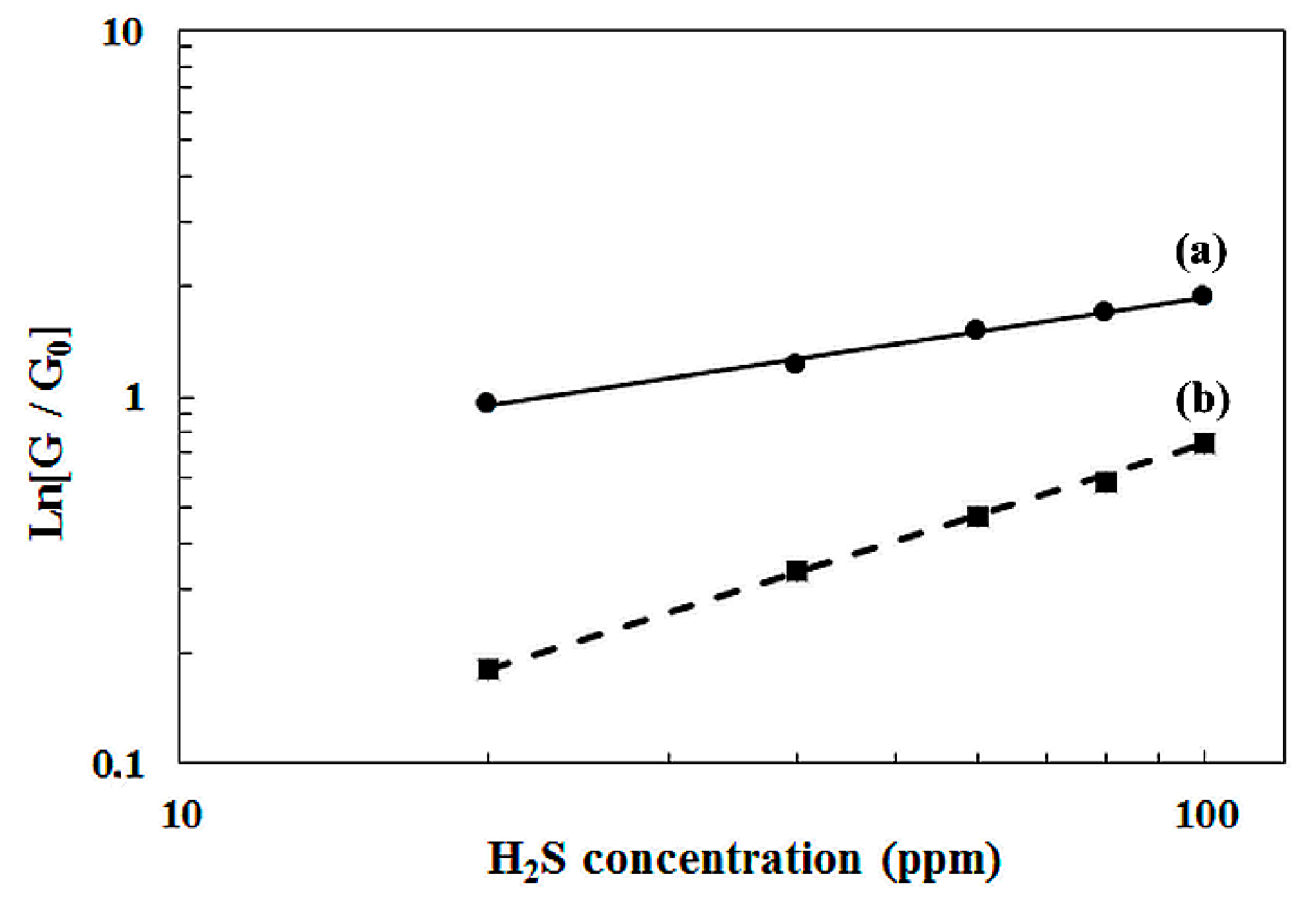
3.4. Measurements under H2S

The sensitivity of semiconductor gas sensors is highly dependent on the operating temperature. In order to determine the optimum operating temperature for the detection of H2S, the sensors were exposed to 100 ppm of H2S at various temperatures. The sensor responses were monitored by using the SIMTRONICS’s measurement system and software. The electrical resistance values of the sensors were extracted from the collected data. An operating temperature ranging from 330 to 450 °C has been chosen for several reasons: (i) in previous tests, our sensors exposed to 100 ppm of H2S have given no significant response at temperatures below 250 °C; (ii) as seen in Section 3.3, the WO3 films present a huge variation of the conductance from 250 to 330 °C; (iii) the maximum operating temperature of our tungsten heater is 500 °C [5].
It is well known that tungsten oxide is an n-type semiconductor, so the sensor conductance increases in the presence of reducing gas such as H2S. Therefore, the sensitivity defined by the ratio G/G0, where G0 and G represent the sensor conductance in air and under gas, respectively, must be higher or equal to unity. Figure 7 shows the sensitivity evolution of sensor-400 (plot (a)) and sensor-500 (plot (b)) to 100 ppm of H2S at various temperatures. The maximum sensitivity is at 350 °C for sensor-400 and 400 °C for sensor-500. Sensor-400 shows a higher sensitivity to H2S than sensor-500. The maximum sensitivity value of sensor-400 is 6.6, whereas it is only 2.4 for sensor-500. This sensitivity of 6.6 is a high value. It means that high-sensitive gas sensors can be manufactured with WO3 thin films annealed at 400 °C. The higher sensitivity value of sensor-400 may be explained by the presence of a lot of very small grains at the surface of the film, as observed in the AFM image from Figure 4. Indeed, many studies have demonstrated that the presence of small grains improves the sensitivity of the film [22,23].

4. Modeling of the Sensitivity Evolution as a Function of the H2S Concentration

Various theories were developed to explain the change in conductance due to the sorption of gas molecules on semiconductor gas sensors. Semiconductor oxides are composed of grains and grain boundaries. The difference of energy levels in this kind of structure implies that the most applied model is based on the Schottky barrier relation [4]. So, considering the Schottky barrier model, the conductance G can be written as follows:
G = A T q k B e x p q Δ ϕ s k B T
where A and kB are the Richardson and Boltzmann constants, q is the electron charge, T is the temperature, and Δϕs is the barrier height. Equation (1) shows that the variation of the conductance depends on the barrier height and temperature. It has been reported [24,25] that the change in barrier height Δϕs can be expressed as a function of the degree of the surface coverage θ:
Δ ϕ s = e N s 2 θ 2 2 ε ε 0 N D
where NS is the number of surface charges per unit area, ND is the number of ionized donor states per unit volume, ε is the permittivity of the semiconductor, and ε0 is the vacuum permittivity. Combining Equations (1) and (2), the following relation between the conductance G and the degree of the surface coverage θ was obtained:
G = A T q k B e x p e 2 N s 2 θ 2 2 ε ε 0 k B T N D
Several adsorption isotherms have proved to be useful for the understanding of the adsorption process. The most frequently used adsorption isotherms are Langmuir, BET (Brunauer, Emmett, and Teller), and Freundlich isotherms [26,27]. The BET isotherm is valid for multilayer adsorption, so it is not suitable for thin film adsorption. In this work, the Langmuir–Freundlich isotherm with a parameter of heterogeneity is employed to introduce the influence of adsorbents on the gas adsorption.
θ = k p 1 + k p ν
where k is the adsorption constant, p is the partial pressure of the gas, and ν is the heterogeneity parameter of the adsorbent with a value ranging between 0 and 1.
Here, kp << 1 due to the used gas pressure, so the expression can be reduced to:
θ = k p ν
Considering the law of perfect gases given in the Equation (6), the relation (7) between the degree of the surface coverage θ and the gas concentration C is obtained.
p = K C
where C is the gas concentration and K′ is a constant.
θ = K C ν
with K = (kK′)ν.
Using Expression (7) in Equation (3), the conductance G can be related to the gas concentration C:
G = A T q k B exp B C a
where B = e 2 N S 2 K 2 2 ε ε 0 k B T N D and a = 2 ν .
So, the sensitivity G/G0, with G0 representing the conductance of the sensor in air i.e., when C = 0, can be expressed as follows:
G / G 0 = exp B C a
The Neperian logarithm of Equation (9) is used to determine the constants B and a:
L n G G 0 = B C a
Finally, the decimal logarithm of Equation (10) can be used to fit the sensitivity evolution:
L o g L n G G 0 =   L o g B + a L o g C
Equation (11) represents the equation of a straight line with the slope (a) and the intercept (LogB). Equation (11) was used to fit the evolution of experimental data. The results are given in Figure 8. The good accordance between the theoretical model and experimental data proves the validity of the Schottky barrier model associated to the Langmuir–Freundlich isotherm for explaining the behavior of the sensitivity. For sensor-400, the value of parameter a is 0.4, and it is 0.9 for sensor-500. As given previously in the text, a = 2ν. Parameter ν is related to the surface coverage θ. For sensor-400, ν = a/2 = 0.2. For sensor-500, ν = a/2 = 0.45. These values of ν, here lower than 1, indicate that the Langmuir–Freundlich isotherm is well adapted to define the adsorption mechanism of the WO3 thin films.

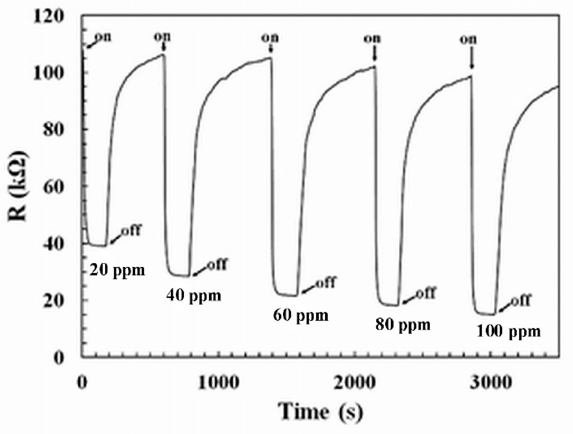
5. Dynamic Response of the Sensors under H2S and Discussion

The dynamic response under H2S pulses at concentration ranging from 20 to 100 ppm for the most sensitive sensor, i.e., sensor-400, is presented in Figure 9. In the presence of H2S, the sensor resistance decreased. This is a typical response for an n-type oxide under reducing gas. The response and recovery times are the time taken to reach 90% of the equilibrium point when gas or air is introduced. The response and recovery times of sensor-400 are about 20 s and 420 s, respectively, under 100 ppm of H2S. The highest concentration of H2S defines the more difficult conditions for the sensor recovery. Indeed, a complete saturation at the highest concentration induces longer recovery times. Effectively, the recovery time decreases to 240 s under H2S 20 ppm.
For sensor-500, the response time is of about 25 s, which is a little bit higher than that for sensor-400, but the recovery time is lower: 150 s under H2S 100 ppm. The dynamic response of sensor-500 is not presented here. The lower recovery time of sensor-500 is linked to its lower sensitivity. Indeed, when the sensitivity variation is higher, the variation of the sensor resistance is higher as well. In this case, the sensor needs more time to recover after the exposition to the gas. Under H2S 20 ppm, sensor-500 presents a response time of about 45 s and 120 s for the recovery time.
For discussing the relevancy of the results given here, some recent works on oxide thin films are cited from the literature and listed in Table 3. On mesoporous WO3 thin films elaborated by sol–gel, a sensitivity of 1.5 and a response time of 100 s were measured for non-doped films under 100 ppm of H2S [28].
On other metallic or complex oxides, interesting results can be found. Under H2S 10 ppm, CaCu3Ti4O12 thin films exhibit a very good sensitivity [32], in particular with the Fe doping, but the recovery times can be longer, from 500 to 1100 s as a function of the Fe-doping rate. With a sensitivity ranging from 2.6 to 6.6 at the operating temperature of 350 °C, while recovery times do not exceed 420 s, the WO3 sensor-400 shows very interesting characteristics. Finally, in order to test its stability and verify the full recovery, the sensor-400 was exposed at first to 50 ppm of H2S at 350 °C during 30 min and then to dry air. A slight decrease in the resistance value of less than 4% was observed. This final test was made after all measurements presented here. That means that these WO3 sensors have a very good reliability and very good achievements under H2S and therefore could be good candidates for an industrial implementation.

6. Conclusions

Tungsten trioxide thin films were elaborated by non-reactive RF magnetron sputtering and annealed at two different temperatures, 400 and 500 °C. The morphology and crystalline structure were studied. The DRX and AFM results suggest that an increase in the annealing temperature mainly affects the morphology of the film. Two sensors, composed of a W heating element, a WO3 sensing element, and W electrodes embedded in a commercial case, were tested under different conditions at SIMTRONICS SAS (3M Company). Sensor-400 has given a higher sensitivity to H2S than sensor-500. This behavior can be linked to the presence of smaller grains in the film annealed at 400 °C. A model of the sensitivity evolution has revealed that the operating conduction mechanism is governed by a Schottky barrier-controlled conduction associated with the Freundlich adsorption isotherm for the adsorption of gases at the sensor surface. Our cost-effective sensors have given interesting results: short response time of about 20 s, quite complete recovery after a long exposure to H2S, and a very good sensitivity of 6.6 (sensor-400). These features demonstrate that the sensors can be applied in industrial conditions. Moreover, the sensors can be qualified as cost-effective sensors because they are only composed of low-cost materials, tungsten and tungsten trioxide, and an industrial technique, i.e., sputtering, was used for the deposition. Finally, these WO3 sensors have really demonstrated their possible use in industrial sites such as oil platforms or oil drilling sites for the detection of hydrogen sulfide.

Author Contributions

Conceptualization, methodology, validation, data curation, writing—original draft preparation, supervision, D.F.; Writing—review and editing, D.F., N.V., S.D.; Preparation of samples, measurements, D.F., N.V.; XRD characterization, S.D. All authors have read and agreed to the published version of the manuscript.

Funding

This research received no external funding.

Institutional Review Board Statement

Not applicable.

Informed Consent Statement

Informed consent was obtained from all subjects involved in the study.

Acknowledgments

We really want to thank: Benoît Duponchel, research engineer at UDSMM Laboratory for his help and participation, and Nicolas Uschanoff, from SIMTRONICS SAS, for his help during the measurements under gas.

Conflicts of Interest

The authors declare no conflict of interest.

References

  1. Pandey, S.K.; Kim, K.-H.; Tang, K.-T. A review of sensor-based methods for monitoring hydrogen sulfide. TrAC Trends Anal. Chem. 2012, 32, 87–99. [Google Scholar] [CrossRef]
  2. Moseley, P. Materials selection for semiconductor gas sensors. Sens. Actuators B Chem. 1992, 6, 149–156. [Google Scholar] [CrossRef]
  3. Heiland, G. Homogeneous semiconducting gas sensors. Sens. Actuators 1982, 2, 343–361. [Google Scholar] [CrossRef]
  4. Morrison, S.R. Semiconductor gas sensors. Sens. Actuators 1982, 2, 329–341. [Google Scholar] [CrossRef]
  5. Verbrugghe, N.; Fasquelle, D.; Duponchel, B.; Deputier, S. Study of tungsten films deposited by DC sputtering dedicated to integrated heaters. J. Vac. Sci. Technol. B 2017, 35, 031204. [Google Scholar] [CrossRef]
  6. Antonik, M.; Schneider, J.; Wittman, E.; Snow, K.; Vetelino, J.; Lad, R. Microstructural effects in WO3 gas-sensing films. Thin Solid Films 1995, 256, 247–252. [Google Scholar] [CrossRef]
  7. Sberveglieri, G.; Depero, L.; Groppelli, S.; Nelli, P. WO3 sputtered thin films for NOx monitoring. Sens. Actuators B Chem. 1995, 26, 89–92. [Google Scholar] [CrossRef]
  8. Moseley, P.T.; Norris, J.O.W.; Williams, D.E. Techniques and Mechanisms in Gas Sensing; 1991; pp. 46–60. Available online: https://www.scienceopen.com/document?vid=7883bc3a-29bc-4934-bab8-0f9dccf51c1a (accessed on 9 September 2021).
  9. Cantalini, C.; Sun, H.T.; Faccio, M.; Pelino, M.; Santucci, S.; Lozzi, L.; Passacantando, M. NO2 sensitivity of WO3 thin film ob-tained by high vacuum thermal evaporation. Sens. Actuators B 1996, 31, 81–87. [Google Scholar] [CrossRef]
  10. Ozer, N.; Lampert, C. Electrochromic performance of sol-gel deposited WO3–V2O5 films. Thin Solid Films 1999, 349, 205–211. [Google Scholar] [CrossRef]
  11. de Tacconi, N.R.; Chenthamarakshan, C.R.; Wouters, K.L.; MacDonnell, F.M.; Rajeshwar, K. Composite WO3-TiO2 films pre-pared by pulsed electrodeposition: Morphological aspects and electrochromic behavior. J. Electroanal. Chem. 2004, 566, 249–256. [Google Scholar] [CrossRef]
  12. Moulzolf, S.C.; Ding, S.-A.; Lad, R.J. Stoichiometry and microstructure effects on tungsten oxide chemiresistive films. Sens. Actuators B Chem. 2001, 77, 375–382. [Google Scholar] [CrossRef]
  13. Khatko, V.; Vallejos, S.; Calderer, J.; Llobet, E.; Vilanova, X.; Correig, X. Gas sensing properties of WO3 thin films deposited by rf sputtering. Sens. Actuators B Chem. 2007, 126, 400–405. [Google Scholar] [CrossRef]
  14. Acosta, M.; González, D.; Riech, I. Optical properties of tungsten oxide thin films by non-reactive sputtering. Thin Solid Films 2009, 517, 5442–5445. [Google Scholar] [CrossRef]
  15. Riech, I.; Acosta, M.; Pena, J.L.; Bartolo-Perez, P. Effects of working pressure on physical properties of tungsten-oxide thin films sputtered from oxide target. J. Vac. Sci. Technol. A 2010, 28, 329. [Google Scholar] [CrossRef]
  16. Woodward, P.M.; Sleight, A.W. Ferroelectric Tungsten Trioxide. J. Solid State Chem. 1997, 131, 9–17. [Google Scholar] [CrossRef]
  17. Lefkowitz, I.; Dowell, M.; Shields, M. Phase transitions in tungsten trioxide at low temperatures. J. Solid State Chem. 1975, 15, 24–39. [Google Scholar] [CrossRef]
  18. Khojier, K.; Savaloni, H.; Habashi, N.; Sadi, M. On the influence of temperature gradient of annealing process on the nano-structure and sensing properties of WO3 thin films to NO2 gas and relative humidity. Mater. Sci. Semicond. Process. 2016, 41, 177–183. [Google Scholar] [CrossRef]
  19. Fasquelle, D.; Verbrugghe, N.; Laasri, H.A.; Tachafine, A.; Duponchel, B.; Députier, S.; Costa, L.C.; Elaatmani, M.; Outzourhit, A.; Carru, J.-C. Promising Performance of Lead-Free Functional thin films and ceramics. J. Phys. Conf. Ser. 2019, 1153, 012064. [Google Scholar] [CrossRef]
  20. Cora, F.; Stachiotti, M.G.; Catlow, C.R.A.; Rodriguez, C.O. Transition Metal Oxide Chemistry: Electronic Structure Study of WO3, ReO3, and NaWO3. J. Phys. Chem. 1997, 101, 3945–3952. [Google Scholar] [CrossRef]
  21. Al Mohammad, A.; Gillet, M. Phase transformations in WO3 thin films during annealing. Thin Solid Films 2002, 408, 302–309. [Google Scholar] [CrossRef]
  22. Gillet, M.; Aguir, K.; Bendahan, M.; Mennini, P. Grain size effect in sputtered tungsten trioxide thin films on the sensitivity to ozone. Thin Solid Films 2005, 484, 358–363. [Google Scholar] [CrossRef]
  23. Wang, S.-H.; Chou, T.-C.; Liu, C.-C. Nano-crystalline tungsten oxide NO2 sensor. Sens. Actuators B Chem. 2003, 94, 343–351. [Google Scholar] [CrossRef]
  24. Geistlinger, H. Electron theory of thin-film gas sensors. Sens. Actuators B Chem. 1993, 17, 47–60. [Google Scholar] [CrossRef]
  25. McAleer, J.F.; Moseley, P.T.; Norris, J.O.W.; Williams, D.E. Tin dioxide gas sensors. Part 1.—Aspects of the surface chemistry revealed by electrical conductance variations. J. Chem. Soc. Faraday Trans. 1 Phys. Chem. Condens. Phases 1987, 83, 1323–1346. [Google Scholar] [CrossRef]
  26. Srivastava, R.K.; Lal, P.; Dwivedi, R.; Srivastava, S. Sensing mechanism in tin oxide-based thick-film gas sensors. Sens. Actuators B Chem. 1994, 21, 213–218. [Google Scholar] [CrossRef]
  27. Sun, H.-T.; Cantalini, C.; Lozzi, L.; Passacantando, M.; Santucci, S.; Pelino, M. Microstructural effect on NO2 sensitivity of WO3 thin film gas sensors. Thin Solid Films 1996, 287, 258–265. [Google Scholar] [CrossRef]
  28. Takács, M.; Pap, A. Gas Sensitivity of Sol-gel Prepared Mesoporous WO3 thin Film. Procedia Eng. 2016, 168, 289–292. [Google Scholar] [CrossRef]
  29. Poongodi, S.; Kumar, P.S.; Mangalaraj, D.; Ponpandian, N.; Meena, P.; Masuda, Y.; Lee, C. Electrodepositon of WO3 nanostruc-tured thin films for electrochromic and H2S gas sensor applications. J. Alloys Compd. 2017, 719, 71–81. [Google Scholar] [CrossRef]
  30. Kim, W.-S.; Kim, H.-C.; Hong, S.-H. Gas sensing properties of MoO3 nanoparticles synthesized by solvothermal method. J. Nanopart. Res. 2009, 12, 1889–1896. [Google Scholar] [CrossRef]
  31. Balouria, V.; Kumar, A.; Samanta, S.; Singh, A.; Debnath, A.; Mahajan, A.; Bedi, R.; Aswal, D.; Gupta, S. Nano-crystalline Fe2O3 thin films for ppm level detection of H2S. Sens. Actuators B Chem. 2013, 181, 471–478. [Google Scholar] [CrossRef]
  32. Pongpaiboonkul, S.; Phokharatkul, D.; Hodak, J.H.; Wisitsoraat, A.; Hodak, S.K. Enhancement of H2S-sensing performances with Fe-doping in CaCu3Ti4O12 thin films prepared by a sol–gel method. Sens. Actuators B Chem. 2016, 224, 118–127. [Google Scholar] [CrossRef]
Figure 1. Gas sensor structure [19].
Chemosensors 09 00295 g001
Figure 2. Images of the manufactured sensor (a) and of the DG-TT7 detection system from Simtronics SAS (b).
Chemosensors 09 00295 g002
Figure 3. XRD spectra of WO3 films annealed at 400 °C (a) and 500 °C (b) for 6 h in air. Peak indexations are related to either triclinic (δ-WO3), monoclinic (γ-WO3), or orthorhombic (β-WO3) structures.
Chemosensors 09 00295 g003
Figure 4. AFM images (2 µm × 2 µm) of WO3 films annealed at 400 °C (a) and 500 °C (b) for 6 h. Insets: zoomed AFM images (500 nm × 500 nm).
Chemosensors 09 00295 g004
Figure 5. AFM images (2 µm × 2 µm) of WO3 films annealed at 400 °C (a) and 500 °C (b) for 6 h, with a numerical treatment.
Chemosensors 09 00295 g005
Figure 6. Evolution of the conductance of the sensor-400 in air versus reciprocal temperature.
Chemosensors 09 00295 g006
Figure 7. Sensitivity of sensor-400 (a) and sensor-500 (b) under 100 ppm of H2S in air as a function of temperature [19].
Chemosensors 09 00295 g007
Figure 8. Sensitivity of sensor-400 (a) and sensor-500 (b) versus the H2S concentration at 350 °C. The dots are experimental values. The lines are the fitting curves obtained with Equation (10).
Chemosensors 09 00295 g008
Figure 9. Dynamic response of sensor-400 under different concentrations of H2S at 350 °C; on: H2S injected; off: air injected.
Chemosensors 09 00295 g009
Table 1. Physical and electrical characteristics of the complete sensor: heater and sensing elements [19].
ElementValue
Substrate dimensions
W film thickness of the heater
8 mm × 4 mm
565 nm ± 35 nm
Heater electrical resistance at 20 °C50 Ω ± 10 Ω
W film thickness of the electrodes
Thickness of WO3 films annealed at 400 and 500 °C
Electrical resistance at room temperature of WO3 films annealed at 400 and 500 °C
300 nm ± 10 nm
120 nm ± 10 nm
5 MΩ ± 1 MΩ
Table 2. Diffraction angle (2θ), interplanar spacing (d), and crystallite size (Lhkl) values of WO3 films annealed at 400 °C and 500 °C.
Annealing Temperature
(°C)
2θ (°)d (Å)Lhkl (nm)(hkl) Plane
40023.26 ± 0.023.82 ± 0.0163 ± 2(002)
24.12 ± 0.023.68 ± 0.0164 ± 2(200)
50023.27 ± 0.023.82 ± 0.0161 ± 2(002)
24.14 ± 0.023.68 ± 0.0177 ± 2(200)
Table 3. Comparison of sensing thin-film materials for H2S monitoring.
Gas Sensing MaterialOperating TemperatureSensitivity
G/G0
Response Time (s)Recovery Time (s)H2S (ppm)Refs.
Mesoporous WO3
Sol–gel
260 °C1.520060100[28]
Nanostructured WO3
electrodeposition
300 °C0.855010010[29]
MoO3 micro-sized commercial powder375 °C3310>80020[30]
Nano-crystalline Fe2O3
E-beam evaporation
250 °C6.264>900050[31]
Fe-doped CaCu3Ti4012
Sol–gel
250 °C1255500–110010[32]
WO3 sensor-400
RF sputtering
350 °C2.6–6.630–20240–42020–100This study
Publisher’s Note: MDPI stays neutral with regard to jurisdictional claims in published maps and institutional affiliations.

