Article

Super Stable Pollution Gas Sensor Based on Functionalized 2D Boron Nitride Nanosheet Materials for High Humidity Environments
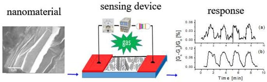
Department of Physics, College of Natural Sciences, University of Puerto Rico, San Juan, PR 00936-8377, USA
*
Author to whom correspondence should be addressed.
Chemosensors 2018, 6(4), 49; https://doi.org/10.3390/chemosensors6040049
Submission received: 28 September 2018 / Revised: 30 October 2018 / Accepted: 1 November 2018 / Published: 3 November 2018

Abstract

:
We report on studies of new gas sensing devices to be used in high humidity environments. Highly thermal-stable, super hydrophobic 2-dimensional (2D) boron nitride nanosheets (BNNSs) functionalized with Pt nanoparticles were prepared and used as an active layer for the prototype. The morphologic surface, crystallographic structures and chemical compositions of the synthesized 2D materials were characterized by using optical microscope, scanning electron microscope (SEM), transmission electron microscope (TEM) and atomic force microscope (AFM) and Raman scattering, respectively. The experimental data reveals that high-quality BNNSs were prepared. A pair of Au electrodes were combined with a basic electrical circuit and the 2D sensing material to form high-performance gas sensors for the detection of pollution gases. The present structure is simple and the fabrication is easy and fast, which ensures the creation of a low-cost prototype with harsh (high humidity, high temperature) environment resistance and potential for miniaturization. The responses of the prototype to different target gases with different concentrations were characterized. The influences of the operating temperature and bias voltage effect on sensing performances were also investigated. The fabricated sensors appear to have high selectivity, high sensitivity and fast response to target gases. The sensing mechanism in the present case is attributed to the electron donation from the target gas molecules to the active layer, leading to the change of electrical properties on the surface of BNNS layer.

Graphical Abstract

1. Introduction

Low concentrations of hazardous gases are difficult to be detected by using common gas sensors. Development of novel materials for the formation of devices optimized for their use for the detection of target gas contaminants while operating in hazardous environments has always been the subject of prime interest. Up to today, many successes on the pollution gas sensors based on low-dimensional nanostructured materials have been achieved and reported [1,2,3,4].
In the one-dimensional (1D) system, various noble metals such as Pt or Au nanowires (NWs) were widely explored as sensing materials for the detection of hydrogen, ethanol, NH3 and other gases [5]. Emphasis was placed on the room temperature operation even if the sensitivity is relatively low [5,6]. Additionally, fabrications of various semiconducting nanowires including oxide semiconductors, Si, diamond or nanocomposite NWs based gas sensing devices were also reported [7,8,9,10]. The two basic approaches, top-down and bottom-up, for synthesizing nanowires were compared [7,11]. The conduction mechanisms, sensing performances, configurations and sensing principles of different nanowire gas sensors were discussed [11]. Special attention was given to extra controls such as metal decoration, local heating and light irradiation, which combined with the gate electrode, can tune the nanowire channel and attain more effective gas sensing [12,13,14,15].
In contrast, 2D nanosheets are another important material for this field due to their extraordinary mechanical and electrical [16,17] and gas sensitive properties [18,19]. For example, the experiments from Cui group clearly indicated that 2D materials could be used to fabricate ultrahigh sensitivity gas sensors [20]. A layer-dependent sensing performance was observed. Our recent experiments also indicated that 2D BN nanosheets based gas sensor had a quick response [21]. Varghese, et al. reviewed the latest advancements with focus on 2D sheets based sensor performance metrics such as sensitivity, specificity, detection limit and the current challenges and future prospects [22].
Despite the fact that theoretical and preliminary experimental studies have predicted the feasibility of 2D materials for sensing devices, few experiments have been carried out. There are no reports related to 2D BNNSs based ultra-sensitivity gas sensing devices that can stand up to high humidity environments. One of the reasons behind this is that the fabrication of such atomically thin BNNSs with highly hydrophobic properties for operation in humid conditions remains a challenge. In fact, gas sensor performance based on random distribution of nanostructured material is usually influenced by environmental conditions. For example, either weak response strength or poor response time was observed because of environmental humidity or the adsorption of external molecules on the surface of nanostructured materials. The adsorption of molecules can lead to less chemisorptions of species on the material surface due to the decrease of the surface areas responsible for the sensors’ sensitivities. The superficial migration of the external water molecule on the sensing material surface becomes difficult; thus the sensitivity decreases and the response and recovery times increase [23,24].
Very recent experiments suggested that the problems above could possibly be solved by using highly ordered 2D nanomaterials. It revealed that properties including the wettability and sensing response of 2D materials not only relies on doping elements, doping concentrations and surface functionalization but also highly depends on oriented nanostructures. This may allow for the design and creation of new antiwetting surfaces with unchanged sensing properties. For example, 2D MoS2 sheets synthesized at 550, 750 and 900 °C yielded very different surface energies (or different static contact angles) that tune its wettability from hydrophilicity to hydrophobicity and then to super hydrophobicity [25]. It was also found that vertical orientation of BNNS films appears to be super hydrophobic and its water drop contact angle can be as large as 155°. In contrast, the contact angle of the BNNSs with horizontal orientation is only 60° [26]. Fundamental characterization using high resolution TEMs indicated that most of the vertically oriented BNNSs have right angles (90°) at edge corners. This suggests that one side of the edge of the BNNS is related to the zigzag structure and the other side is related to the armchair type of structure. Detailed discussion of edge structures can be found in our previous report [27]. It is expected that the selected two-dimensional materials can be tailored to offer high sensitivity to gases of interest while working in humid conditions.
The focus of the present work is on the synthesis and functionalization of wide bandgap, oriented 2D BNNS materials to achieve a highly stable, highly sensitive material for development of high-performance gas sensor for detection of pollution gases. A set of measurements and strategies was used to understand the mechanisms involved in their gas sensing response. The clarification of such processes brings important information on how these mechanisms are altered in the presence of high humidity and interfering gas contaminants.

2. Experimental Details

The laser plasma deposition (LPD) system used to synthesize 2D BNNSs consists of a high power CO2 pulse laser, a beam delivery system and a vacuum chamber. Detailed description of the LPD system can be found in our previous paper [28]. Briefly, a 30 cm focal length ZnSe lens was used to focus the 10.6 µm CO2 laser beam onto the BN target at a 45° angle with respect to the surface normal. The pyrolytic hexagonal boron nitride target of 2″ dia. × 0.125″ thick, with a purity of 99.9% and a density of 1.94 g/cm3, was mounted on a stage of six-axis adjustment (x, y, z, tip, tilt and rotation at 200× rpm along its surface normal). The focused laser beam, 4 J per pulse at 5 Hz repetition rate, has a spot size of ~2 mm in diameter on the surface of the target, corresponding to a laser power density around 108 W/cm2 per pulse.
Si wafers were chosen as the substrate for the deposition of BNNSs. After the vacuum chamber was loaded, a pressure as low as 10−6 Torr was reached and the substrate temperature was maintained at 400 °C during deposition. Because the laser-produced plasma deposition contains both ionic and molecular deposition [29,30], the distance between the target material and the substrate is one of the important parameters in the deposition process. In the present experiments, the substrates were placed 4 cm away from the plasma source and the duration of each deposition was around 15 min. The nanoscale morphologies of BNNSs were characterized by using optical microscope, scanning electron microscope (SEM), energy dispersive X-ray analyzer (EDS), high-resolution transmission electron microscopy (TEM) and atomic force microscope (AFM).
In the laboratory, SEM (Horiba, Ltd., Albany, NY, USA) was in combination with an EDS operating in an ultra-high vacuum condition to achieve clear SEM observation and accurate EDS analysis. AFM was used for determining surface topography at subnanometer resolution. The technique involves imaging a sample with a probe with a radius of 20 nm. The tip was held several nanometers above the surface using a feedback mechanism that measures surface–tip interactions on the scale of nano Newtons. Variations in tip height were recorded while the tip was scanned repeatedly across the sample, producing a topographic image of the surface. HRTEM was based on the transmitted and the scattered beams to create an interference image. In this case, the outgoing modulated electron waves at very low angles interfered with itself during propagation through the objective lens. All electrons emerging from the specimen were combined at a point in the image plane. HRTEM makes it perfect for imaging materials on the atomic scale. A main advantage of a HRTEM over other microscopes is that it can simultaneously give information in real space and reciprocal space.
The properties were then characterized by using room temperature micro-Raman Spectroscopy equipped with a Jobin–Yvon T64000 Triplemate system (HORIBA Scientific, Edison, NJ, USA) and a radiation of 514.5 nm from a coherent argon ion laser. A liquid nitrogen cooled charge-coupled device system was used to collect and process the scattered data [31]. Characterizations of the wettability or surface energy properties of the sensing materials were based on a water drop contact angle test. The current–voltage relationships at different temperatures were characterized by using two HP34401 multimeters. Finally, BNNSs-based gas sensing devices were designed, fabricated and tested under open-air atmospheric pressure conditions. Vacuum pump Edwards 8 was used to pump out air and the target gas. Target gas was controlled by using a gas flowmeter (gas flow rate can be controlled from 0.01 to 0.2 LPM). Pump and air flow rate remained unchanged. Target gas concentrations was determined based on the ratio between the target gas and the air. The concentrations in the chamber were controlled by adjusting gas flow rates.

3. Results and Discussions

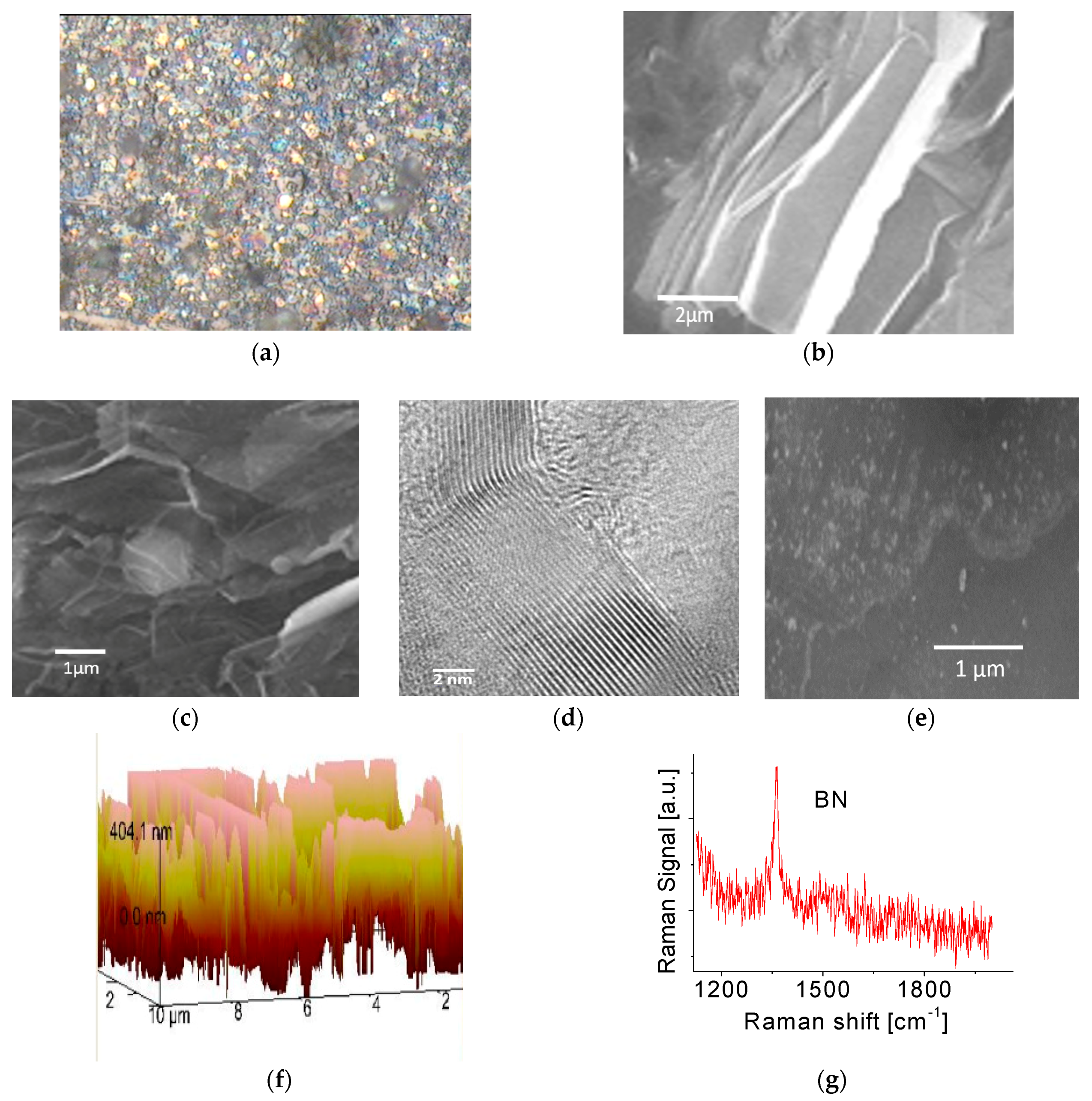
3.1. Basic Characterization of the 2D BNNS Materials

Figure 1a shows a typical optical microscope image of the BNNS film deposited on Si wafer substrate. The obtained film appears to have a rough surface. It reflects no specular light as the light is scattered in all directions and therefore appears dull. Figure 1b,c show SEM images of the BNNS film. No perfectly flat surfaces in nanoscale were clearly visible. The sample normally consists of a large amount of BNNSs with a wide range of distribution in thicknesses and orientations. Average size of each continuous BNNS piece is at a few square micrometer level. From Figure 1c, one can easily find that the fabricated BNNSs have highly transparent properties, probably indicative of its good crystalline structures. This was confirmed by electron diffraction (ED) pattern measurements [32]. The experiments with high-resolution TEM (HRTEM) techniques were carried out to further confirm this conclusion. The result is shown in Figure 1d where tiny, highly ordered fringes at the edge of the sheet is clearly visible. All the fringes have almost the same orientations. Each fringe is related to a single atomic layer and thickness of a single atomic layer is around 0.33 nm. Accordingly, the thickness of the obtained BNNS is 7~9 nm. A statistical analysis of HRTEM images performed on BNNS samples produced by PLD already showed that 75% of BNNSs presented in the films were around 4 to 5 nm in thickness and the remaining 25% were larger than 8 nm [32]. It is noticed that each fringe (Figure 1d) does not appear straight, suggesting a curved sheet structure. This is in good agreement with the data obtained from SEM measurements. Figure 1e shows SEM image of functionalized BNNS film. Nanoparticles on the surface of the film can be easily identified. Functionalization of BNNSs with Pt nanoparticles was carried out in a plasma sputtering chamber. In the present work, nano metal particles were directly deposited onto the surface of the BNNS sample. The energy-dispersive X-ray spectroscopy (EDS) measurements indicated that the Pt concentration was around ~1 At %. Different surface morphologies before and after functionalization are readily visible.
In order to understand the spatial orientations of the BNNSs, an AFM measurement was also carried out and the result is presented in Figure 1f. As observed in the figure, numerous nanostructures representing individual BNNSs in the film have a wide range of orientations including vertically aligned BNNS array pattern. This feature may affect BNNS film surface energy and/or its hydrophobic properties, which would be discussed in next section.
Raman scattering measurements were performed at room temperature where the microscope focused the laser beam onto the surface of the sample. [31] A Raman active E2g mode of the BNNS film at ~1363 cm−1 was observed as shown in Figure 1g, indicating it is a hexagonal phase. Slightly unsymmetrical structure or profile of the spectral line likely indicates that impurities were presented in the BNNSs. This possibly stemmed from the residual gas in the chamber or was due to oxygen adsorption during the transport of the samples.
Characterizations of the wettability or surface energy properties of the sensing material were based on simple measurements of the water drop contact angle. Figure 2 shows a typical optical image of a water drop on the surface of BNNS sensing material, from which the water drop contact angle was estimated to be around 100°, indicating that the hydrophobic surface has been achieved. However, superhydrophobic properties of the surface has not yet been observed. This might be due to the fact that there are no perfectly vertical orientations of BNNS arrays as shown in Figure 1 with AMF and SEM measurements. Nevertheless, the obtained static contact angle is still much larger than that of horizontal orientations of the BNNS film.

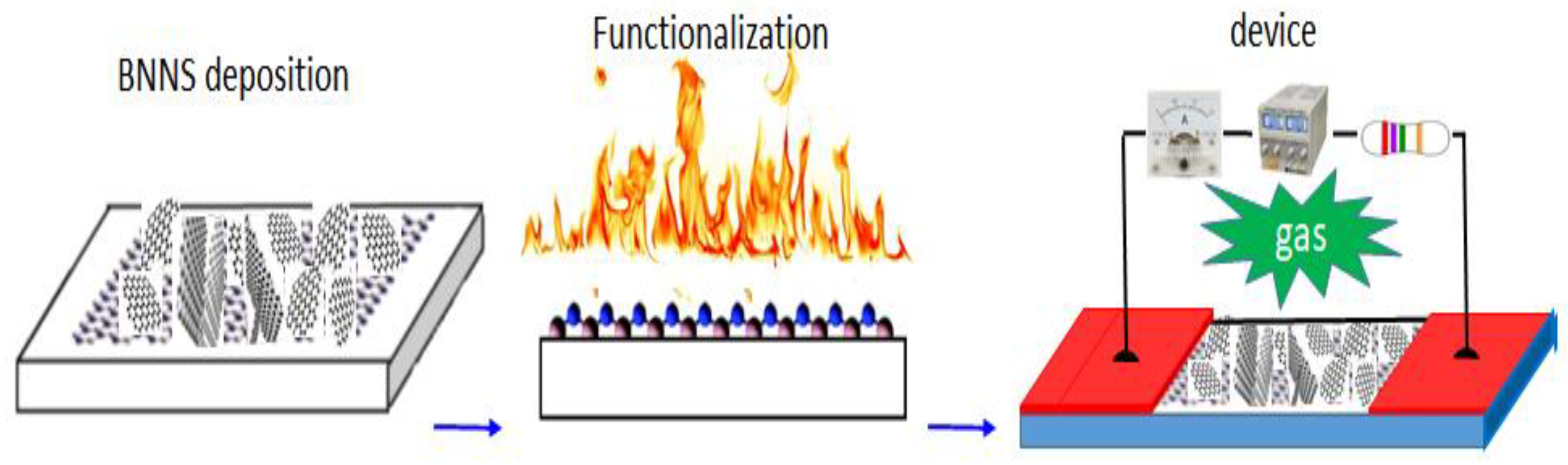
3.2. Fabrication of Prototype and Characterization of Its Electrical Properties

There is a lot of published data in the literature measuring sensor response time in high humidity environments. A typical example is featured in Yamaguchi’s work [33]. In general, the sensing property declined in humid atmospheres because water molecules adsorbing on the film surface disturbed the catalytic reaction between hydrogen and Pt. Relative humidity had variable impacts on the sensor response [34]. For this reason, the focus of the present paper was on achieving a controllable surface orientation with super hydrophobic properties for operation in humid conditions. This is very different from previous work.
The process flow for the fabrication of an oriented BNNSs based gas sensor is presented in Figure 3. BNNSs based membrane with a thickness of around 2–3 µm is used as an active layer. Functionalization of BNNS with Pt nanoparticles (NPs) was carried out in a plasma sputtering chamber. After that, 70~80 nm thick Au films as electrodes were deposited in two ends of the BNNS active layer. The total exposure area of the active layer is 0.8 × 4 mm2. Finally, the active layer was combined with a basic electrical circuit to form a prototypic gas sensor. The present structure is simple and the fabrication is easy. After annealing at 150 °C for one hour, the prototype was electrically characterized first and followed by the measurements of responsivity to different gases.
It should be mentioned that the present sample annealing at 150 °C was based on the following two facts: (1) Annealing helps to clean workpieces. Annealing was not for recrystallization; (2) crack formation in the interface was avoided during annealing. SEM image of the surface morphology of BNNS/Mo appears to have evident cracks at 300–400 °C annealing. The general understanding is that when residual stresses of the over layer are sufficiently high, crack patterns are likely to develop. The minimum stress level to cause cracking is determined by mechanic properties of both over layer and substrate. For this reason, we did not anneal the sample at very high temperature.
The measurements of electrical properties of samples were carried out in open-air ambient conditions. Figure 4 shows typical current–voltage characteristics of the prototype operating at 25, 50, 80 and 120 °C, respectively. The obtained curves show typical linear behaviors. This is attributed to the fact that the surface of the BNNS has been heavily treated with Pt nanoparticles. A high concentration of dopant or treatment normally induces the narrow depletion region at the interface between the metal and the semiconductor. As a result, the tunneling effect would happen and then the tunneling current would be dominated, leading to small contact resistance. In other words, it yields good ohm contact.
Experimental data indicated that a slight increase of operating temperature does not significantly affect the electrical current-voltage curves. The slopes of the current-voltage curves (or resistances) of treated BNNSs remain almost unchanged following an increase of temperature up to 80 °C and the change in electrical conductivity is less than 4% after temperature is increased up to 120 °C. These features provide direct evidence that BNNS materials have very good electrical properties that is nearly independent on temperature varying from 20 to 100 °C. This makes it promising material for wide electronic device applications.

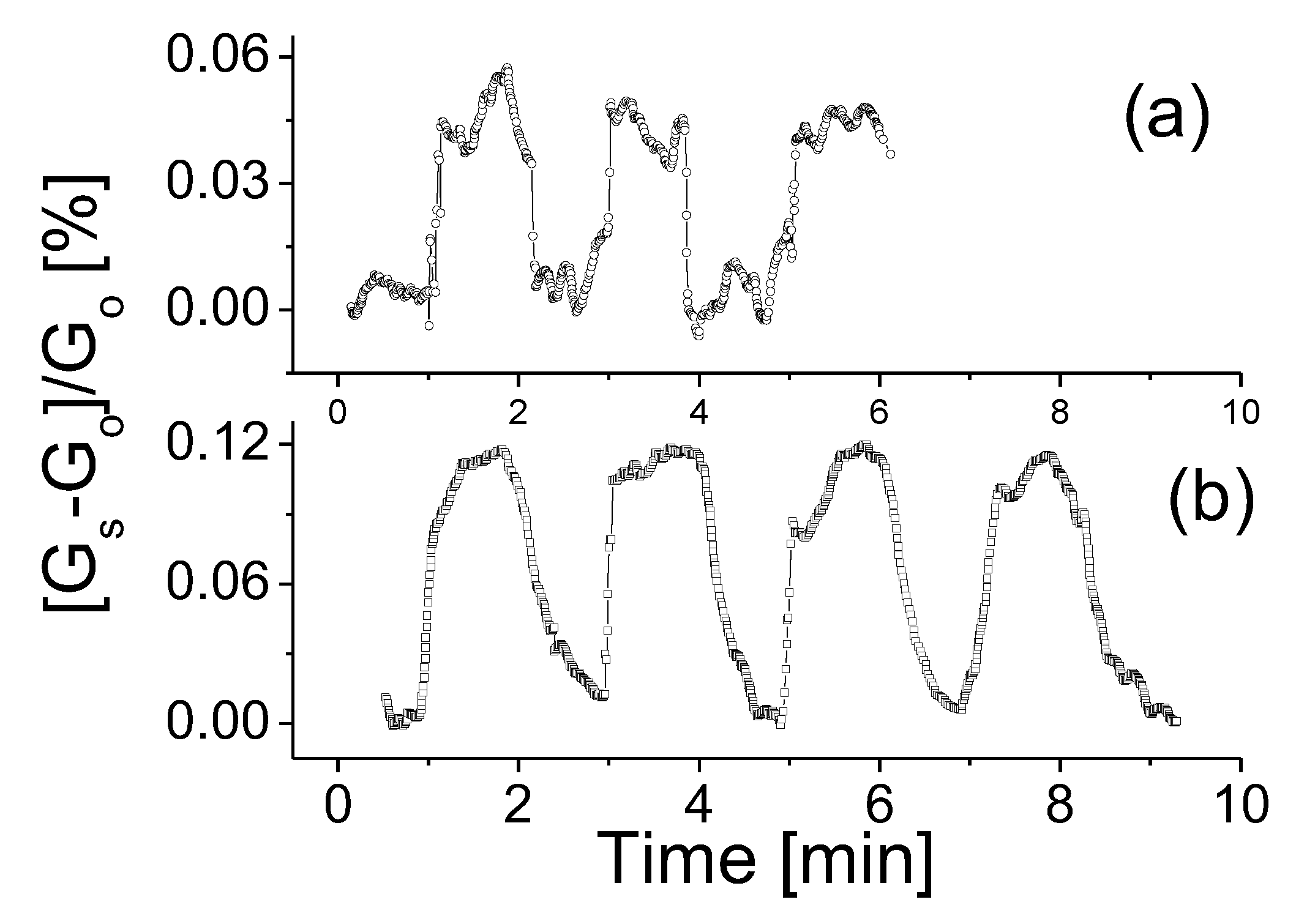
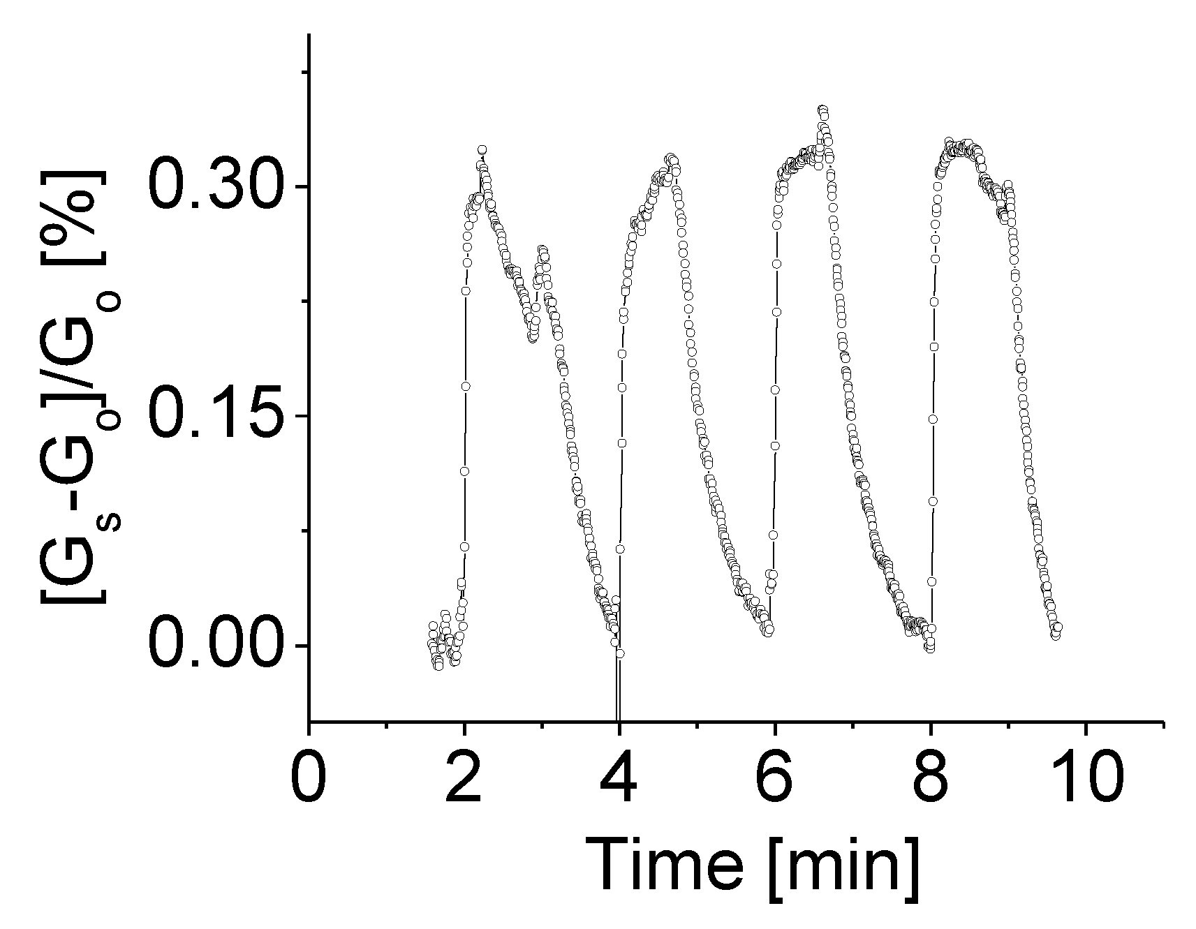
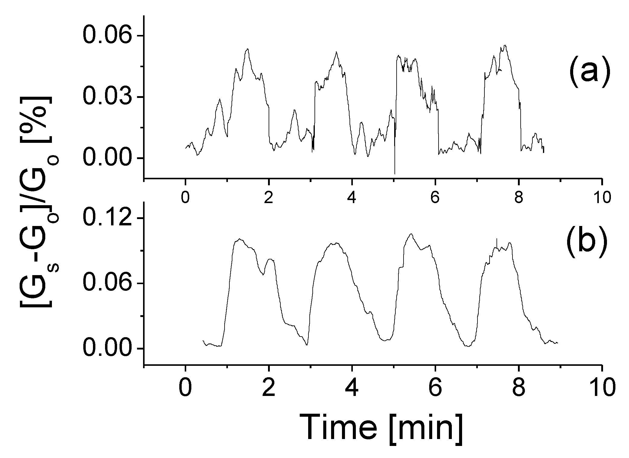
3.3. Response to Target Gases with Different Concentrations

After fabrications, characterizations of the responses of the prototype were carried out under open-air atmospheric pressure conditions. Two types of small molecules, H2 and CH4 target gases, were selected and mixed with air gas, respectively. The prototype was placed into a chamber with a constant gas flow rate and the valves were then switched to target gas/air mixture.
Theoretical estimation of the adsorption energies of these gases on the surface of BN cluster has already been carried out [35]. The interaction between these molecules and the BN cluster can induce changes to the sensing material electronic properties so that its bandgap is decreased, leading to an increment in the electrical conductivity of the cluster. Thus, theoretical work suggested that the BN nanomaterial could be used as a gas-sensing device.
Figure 5 shows the typical results of a sensing response cycling test of the BNNSs based gas sensor toward H2 gas at two different concentrations. When the prototype was exposed to H2 target gas, the induced conductivity risen at first and then reached a stable state. When the valve for the target gas was tuned off, the induced conductivity decreased quickly and then gradually recovers to its original state. The variations in conductivity could be directly attributed to the absorption of external gas molecule. The external gas and BN interaction was considered as physisorption with a weak bond.
As seen, the prototype has good features in repeatability and stability. The obtained maximum relative response to 200 ppm H2 is around 0.06 at 0.5 V bias voltage and room temperature. The definition of the response is based on the ratio between the conductivity change induced with the target gas and the original conductivity: (Gs − Go)/Go, where Gs refers to the conductivity with mixture gas and Go represents the original conductivity of the sensor in air. Following an increase of gas concentration from 200 ppm to 2000 ppm, the yielded response strength increases up to 0.1 as shown in Figure 5b. The weak response signal might be caused by the low bias voltage applied. For this reason, we would carry out additional experiments on studies of bias voltage effect and temperature effects on the performance of the device.
It was found from Figure 5 that the response time is slightly long, around 20–30 s at high concentrations of the target gas and that it becomes much shorter, around 4–8 s at low concentrations. In contrast, the recovery time remained almost unchanged regardless of low or high concentrations. The repeated measurements were also conducted and the obtained data confirmed that high signal-to-noise ratio could be obtained at a high concentration target gas. The relative error should be significantly less than 20%.
The difference in response time depends on many factors such as the type of target gases, concentrations, operating temperatures, bias voltage and environment, among others. In general, the response time of the prototype was estimated around 6 s and the recovery time was around 25 s. True response and recovery times might be shorter because of the delay in reaching the desired concentrations after switching on or off the target gas source.
It should be pointed out that the tests were carried out at relative humidity (RH) level of around 55% and 75%, respectively. No obvious change in response signal was observed, although the sensor appeared to have a slightly longer response time at high RH level. The gas mixtures exhibiting maximum deviation were composed of molecules that had significantly different molecular weights from each other. The detailed mechanism of this phenomenon is still not clear but a tentative interpretation is that the random motions and collisions of target gas with water molecules in high humidity environments can affect target molecular mean free path and shift spend [36]. This might have an impact on sensor response time.
As a comparison, characterizations were also carried out with the prototype exposed to CH4 gas. Figure 6 shows the responses of the prototype to CH4 gas with concentrations of (a) 200 ppm and (b) 2000 ppm. The prototype seems to have a slightly stronger response compared to that exposed to H2 gas at the same operating temperature and gas concentration. Furthermore, the response time shown in Figure 6a also appeared to be shorter. As CH4 concentration was increased, the response time and recovery time remained nearly unchanged but the response strength of the device reached up to 0.12, which was notably higher than that to H2 gas. This phenomenon seems to contradict the theoretical estimations that the adsorption energy of H2 molecules is marginally higher than that of CH4 molecules [35]. One possible underlying reason may be that the nanotube cluster model used in theoretical calculation is inapplicable to the nanosheet case [35,37]. Further theoretical and experimental studies are needed.

3.4. Bias Voltage Effect

A comparison of sensitivities at different levels of bias voltage was also carried out. Figure 7 shows the response of the prototype at room temperature, 1.0 V bias voltage to H2 gas with concentration of 2000 ppm. The response variation following the target gas on-off cycles was easily identified. Higher bias voltage yielded a higher response. A slight increase of the bias voltage from 0.5 V to 1.0 V resulted in three times high in response rate. The obtained clean response signal with a high signal-to-noise ratio and a well-defined and stable baseline as shown in Figure 7 could be directly attributed to the influence of applied high bias voltage on the sensing device. This is because the bias voltage controls the electron density at the boundaries, which in turn controls the electron trapping process. Combination of the conduction and the trapping model results in special I–V characteristics. Sensitivity is derived from I–V curves, which are largely influenced by trapping.

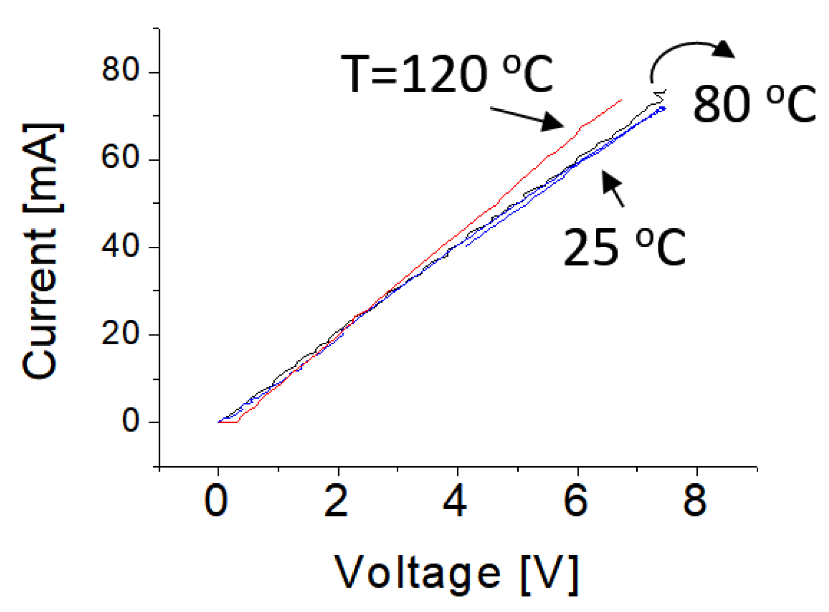
3.5. Temperature Effect

In addition to bias voltage effect, experiments were also carried out to investigate an effect of temperature on the properties of BNNSs based sensing devices. A heater was employed to provide the desired temperature, while all other parameters remained unchanged. Figure 8 shows the response of the prototype at operating temperature of 80 °C, bias voltage of 1.0 V to H2 gas with concentration of 2000 ppm. As seen the response strength of the fabricated sensors significantly increases with temperature.
The general understanding of this mechanism is that the high temperature enhances molecular gas dissociation on the surface of the sensing layer, thus improving catalytic activity. It is anticipated that the target gas then reacts rapidly with agents presented on the surface, resulting in an increase of sensitivity with temperature [38]. It is notable from Figure 8 that the H2 gas-induced conductivity or response at 80 °C is almost 30 times higher than that operating at room temperature. Good features such as stable baseline, good repeatability and low thermal noise strength are clearly visible. A high operating temperature does not, however, improve the response time and recovery time by much.

3.6. Sensing Mechanism

The sensing mechanism in the present case is attributed to the electron donation from the target gas molecules to the active layer, leading to a change in electrical properties on the surface of the BNNS. The density functional theory (DFT) has widely been used to estimate the adsorption energies of H2 and CH4 molecules on the surface of BN cluster. The interactions between these molecules and the BN cluster induce changes to the BN cluster’s electronic properties so that the bandgap width of the cluster decreases, leading to increased electrical conductivity of the cluster [35]. However, theoretical calculations also indicated that a well-structured, such as a perfect BNNT is, in fact, not a good sensing material for the detection of hydrogen and methane gases by either physical or chemical absorption mechanisms [39]. In contrast, nanostructures such as defective nanotubes or 2D sheets in BN were predicted to be of prime importance. Preliminarily theoretical studies have been performed based on DFT within the generalized gradient approximation [40]. Nine possible configurations were selected for a methane molecule approaching the center of the heptagon, hexagon and pentagon of B and N atoms via its –CH, –CH2 and –CH3 groups. The introduction of defects in the BN significantly enhances methane adsorption.
Pt nanoparticles are normally considered to be a promising electrocatalyst. Recent experiments have shown that the catalytic action of Pt nanoparticle additions can powerfully improve gas sensor response and performance [41,42,43]. When H2 (or CH4) gas interacts with sensor surface, the dispersed Pt nanoparticles dissociate target molecules into atomic hydrogen (or –CH, –CH2 and –CH3 groups) which spills over the surface reacting with chemisorbed boron or nitrogen atoms.
In theory, there have been many studies of the interactions of small molecules including CH4 and H2 with BN nanocluster. In fact, BN nanomaterials have attracted considerable attention due to its potential application for hydrogen storage [44].
Based on DFT, several models including B-N-H, H-B-N, H-B-N-H were studied. It was found that the adsorption of atomic hydrogen at N sites is even more unstable than adsorption at B sites in hexagonal boron nitride (h-BN). Further, the adsorption on boron atoms causes a local sp2 to sp3 transformation, whereas adsorption on nitrogen atoms does not occur [45]. This result is in good agreement with the data obtained from specific spectroscopies, that is, near-edge X-ray absorption fine structure (NEXAFS) spectroscopy and X-ray photoelectron spectroscopy (XPS) [46,47]. This is because only the model in which an H atom is attached on a B site consistently explained the experimental results that the B K-edge NEXAFS spectra showed a significant change, while the N K-edge NEXAFS spectra showed little change. Hydrogenation would effectively affect the bandgap width, resulting in an increase of conductivity of BNNS sensing materials [19].

4. Conclusions

Even if theoretical estimations predict that the adsorption energies of target gases on the surface of BN cluster is relatively weak, our experiments demonstrated that a BNNSs based gas sensor has excellent performances including quick response time, good response strength, stable baseline and repeatability. This was attributed to the fact that the surface of the BNNS was functionalized by using Pt nanoparticles to enhance the sensitivity.
It was found that the response strength of the prototype exposed to CH4 target gas was higher than that to H2 gas, at the same gas concentration. Typically, the response time of the prototype is around 6 s and the recovery time is around 25 s.
It was concluded that an increase of applied bias voltage from 0.5 V to 1 V would notably enhance device response strength and improve signal-to-noise ratio. Moreover, a slight increase of operating temperature up to 80 °C could result in a significant increase of device sensitivity up to 30 times higher than that operating at room temperature.

Author Contributions

P.X.F. contributed to design of the experiments, the data analysis, data interpretation and writing the manuscript. E.C. and C.M. provided a contribution on discussion. All authors contributed to analyses of the results in the manuscript.

Acknowledgments

This work is financially supported by NSF-CREST Center for Innovation, Research and Education in Environmental Nanotechnology (CIRE2N) Grant Number HRD-1736093. Authors also acknowledge partial assistance from R.V., M.S., O.R., O.A. and A.G.O. during characterizations and measurements.

Conflicts of Interest

The authors declare no conflict of interest.

References

  1. Kim, Y.H.; Phan, D.T.; Ahn, S.; Nam, K.H.; Park, C.M.; Jeon, K.J. Two-dimensional SnS2 materials as high-performance NO2 sensors with fast response and high sensitivity. Sens. Actuators B Chem. 2018, 255, 616–621. [Google Scholar] [CrossRef]
  2. Han, D.; Yang, W.; Gu, F.; Wang, Z. A low temperature NO2 gas sensor based metal-thiourea complex nanowires. Sens. Actuators B Chem. 2018, 255, 1139–1146. [Google Scholar] [CrossRef]
  3. Asres, G.A.; Baldoví, J.J.; Dombovari, A.; Järvinen, T.; Lorite, G.S.; Mohl, M.; Shchukarev, A.; Paz, A.P.; Xian, L.; Mikkola, J.P.; et al. Ultrasensitive H2S gas sensors based on p-type WS2 hybrid materials. Nano Res. 2018, 11, 4215–4224. [Google Scholar] [CrossRef]
  4. Shao, L.; Wua, Z.; Duan, H.; Shaymurat, T. Discriminative and rapid detection of ozone realized by sensor array of Zn2+ doping tailored MoS2 ultrathin nanosheets. Sens. Actuators B Chem. 2018, 258, 937–946. [Google Scholar] [CrossRef]
  5. Lal, N. Room Temperature Gas Sensing with Ultrathin Au Nanowires. J. Mater. Sci. Eng. 2016, 5, 1000241. [Google Scholar] [CrossRef]
  6. Joshi, N.; Hayasaka, T.; Liu, Y.; Liu, H.; Oliveira, O.; Lin, L. A review on chemiresistive room temperature gas sensors based on metal oxide nanostructures, graphene and 2D transition metal dichalcogenides. Microchim. Acta 2018, 185, 213. [Google Scholar] [CrossRef] [PubMed]
  7. Cao, A.; Sudhölter, E.J.R.; de Smet, L. Silicon Nanowire-Based Devices for Gas-Phase Sensing. Sensors 2014, 14, 245–271. [Google Scholar] [CrossRef] [PubMed]
  8. Peng, X.; Chu, J.; Wang, L.; Duan, S.; Feng, P. Boron-doped diamond nanowires for CO gas sensing application. Sens. Actuators B Chem. 2017, 241, 383–389. [Google Scholar] [CrossRef]
  9. Cardoza-Contreras, M.N.; Romo-Herrera, J.M.; Ríos, L.A.; García-Gutiérrez, R.; Zepeda, T.A.; Contreras, O.E. Single ZnO Nanowire-Based Gas Sensors to Detect Low Concentrations of Hydrogen. Sensors 2015, 16, 30539–30544. [Google Scholar] [CrossRef] [PubMed]
  10. Wan, Q.; Li, Q.H.; Chen, Y.J.; Wang, T.H.; He, X.L.; Li, J.P.; Lin, C.L. Fabrication and ethanol sensing characteristics of ZnO nanowire gas sensors. Appl. Phys. Lett. 2004, 84, 3654–3656. [Google Scholar] [CrossRef]
  11. Chen, X.; Wong, C.K.Y.; Yuan, C.A.; Zhang, G. Nanowire-based gas sensors. Sens. Actuators B Chem. 2013, 177, 178–195. [Google Scholar] [CrossRef]
  12. Wang, L.; Wang, S.; Xua, M.; Hua, X.; Zhang, H.; Wang, Y.; Huang, W. An Au-functionalized ZnO nanowire gas sensor for detection of benzene and toluene. Phys. Chem. Chem. Phys. 2013, 15, 17179–17186. [Google Scholar] [CrossRef] [PubMed]
  13. Lupan, O.; Postica, V.; Labat, F.; Ciofini, I.; Pauporte, T.; Adelung, R. Ultra-sensitive and selective hydrogen nanosensor with fast response at room temperature based on a single Pd/ZnO nanowire. Sens. Actuators B Chem. 2018, 254, 1259–1270. [Google Scholar] [CrossRef]
  14. Qiang, X.; Hu, M.; Zhao, B.; Qin, Y.; Zhang, T.; Zhou, L.; Liang, J. Preparation of porous silicon/Pd-loaded WO3 nanowires for enhancement of ammonia sensing properties at room temperature. Mater. Sci. Semicond. Process. 2018, 79, 113–118. [Google Scholar] [CrossRef]
  15. Feng, P.; Shao, F.; Shi, Y.; Wan, Q. Gas Sensors Based on Semiconducting Nanowire Field-Effect Transistors. Sensors 2014, 14, 17406–17429. [Google Scholar] [CrossRef] [PubMed] [Green Version]
  16. Gupta, A.; Sakthivel, T.; Seal, S. Recent development in 2D materials beyond graphene. Prog. Mater. Sci. 2015, 73, 44–126. [Google Scholar] [CrossRef]
  17. Frisenda, R.; Navarro-Moratalla, E.; Gant, P.; Pérez De Lara, D.; Jarillo-Herrero, P.; Gorbachev, R.V.; Castellanos-Gomez, A. Recent progress in the assembly of nanodevices and van der Waals heterostructures by deterministic placement of 2D materials. Chem. Soc. Rev. 2018, 47, 53–68. [Google Scholar] [CrossRef] [PubMed] [Green Version]
  18. Sun, P.; Ma, R.; Sasaki, T. Recent progress on exploring exceptionally high and anisotropic H+/OH ion conduction in two-dimensional materials. Chem. Sci. 2018, 9, 33–43. [Google Scholar] [CrossRef] [PubMed]
  19. Chen, W.; Li, Y.; Yu, G.; Li, C.Z.; Zhang, S.B.; Zhou, Z.; Chen, Z. Hydrogenation: A Simple Approach to Realize Semiconductor−Half-Metal−Metal Transition in Boron Nitride Nanoribbon. J. Am. Chem. Soc. 2010, 132, 1699–1705. [Google Scholar] [CrossRef] [PubMed]
  20. Cui, S.; Pu, H.; Wells, S.A.; Wen, Z.; Mao, S.; Chang, J.; Hersam, M.C.; Chen, J. Ultrahigh sensitivity and layer-dependent sensing performance of phosphorene-based gas sensors. Nat. Commun. 2015, 6, 8632. [Google Scholar] [CrossRef] [PubMed] [Green Version]
  21. Sajjad, M.; Feng, X.P. Study the Gas Sensing Properties of Boron Nitride Nanosheets. Mater. Res. Bull. 2013, 49, 35–38. [Google Scholar] [CrossRef]
  22. Varghese, S.S.; Varghese, S.H.; Swaminathan, S.; Singh, K.K.; Mittal, V. Two-Dimensional Materials for Sensing: Graphene and Beyond. Electronics 2015, 4, 651–687. [Google Scholar] [CrossRef] [Green Version]
  23. Aldalbahi, A.; Li, E.; Rivera, M.; Velazquez, R.; Altalhi, T.; Peng, X.; Feng, P.X. A new approach for fabrications of SiC based photodetectors. Sci. Rep. 2016, 6, 23457. [Google Scholar] [CrossRef] [PubMed] [Green Version]
  24. Chen, S.F.; Aldalbahi, A.; Feng, P.X. Nanostructured tungsten oxide composite for high-performance gas. Sensors 2015, 15, 27035–27046. [Google Scholar] [CrossRef] [PubMed]
  25. Gaur, A.P.S.; Sahoo, S.; Ahmadi, M.; Dash, S.P.; Guinel, M.J.-F.; Katiyar, R.S. Surface Energy Engineering for Tunable Wettability through Controlled Synthesis of MoS2. Nano Lett. 2014, 14, 4314–4321. [Google Scholar] [CrossRef] [PubMed]
  26. Yu, J.; Qin, L.; Hao, Y.; Kuang, S.; Bai, X.; Chong, Y.-M.; Zhang, W.; Wang, E. Vertically Aligned Boron Nitride Nanosheets: Chemical Vapor Synthesis, Ultraviolet Light Emission, and Superhydrophobicity. ACS Nano 2010, 4, 414–422. [Google Scholar] [CrossRef] [PubMed]
  27. Zhang, Z.; Guo, W.; Yakobson, B.I. Self-modulated band gap in boron nitride nanoribbons and hydrogenated sheets. Nanoscale 2013, 5, 6381–6387. [Google Scholar] [CrossRef] [PubMed]
  28. Sajjad, M.; Peng, X.Y.; Chu, J.; Zhang, H.X.; Feng, P.X. Design and Installation of CO2-pulsed laser plasma deposition system for the synthesis of mass product nanostructure. J. Mater. Res. 2013, 28, 1747–1752. [Google Scholar] [CrossRef]
  29. Bogaerts, A.; Aghaei, M.; Autrique, D.; Lindner, H.; Chen, Z.; Wendelen, W. Computer simulations of laser ablation, plume expansion and plasma formation. Adv. Mater. Res. 2011, 227, 1–10. [Google Scholar] [CrossRef]
  30. Keidar, M.; Fan, J.; Boyd, I.D.; Beilis, I.I. Vaporization of heated materials into discharge plasmas. J. Appl. Phys. 2001, 89, 3095–3098. [Google Scholar] [CrossRef] [Green Version]
  31. Aldalbahi, A.; Rivera, M.; Rahaman, M.; Zhou, A.F.; Mohammed, A.W.; Feng, P. High-performance and self-powered deep UV photodetectors based on high quality 2D boron nitride nanosheets. Nanomaterials 2017, 7, 454. [Google Scholar] [CrossRef] [PubMed]
  32. Sajjad, M.; Ahmadi, M.; Guinel, M.J.-F.; Lin, Y.; Feng, P. Large-scale synthesis of single-crystal and polycrystalline boron nitride nanosheets. J. Mater. Sci. 2013, 48, 2543–2549. [Google Scholar] [CrossRef]
  33. Yamaguchi, Y.; Imamura, S.; Nishio, K.; Fujimoto, K. Influence of temperature and humidity on the electrical sensing of Pt/WO3 thin film hydrogen gas sensor. J. Ceram. Soc. Jpn. 2016, 124, 629–633. [Google Scholar] [CrossRef]
  34. Wei, P.; Ning, Z.; Ye, S.; Sun, L.; Yang, F.; Wong, K.C.; Westerdahl, D.; Louie, P.K.K. Impact Analysis of Temperature and Humidity Conditions on Electrochemical Sensor Response in Ambient Air Quality Monitoring. Sensors 2018, 18, 59. [Google Scholar] [CrossRef] [PubMed]
  35. Beheshtian, J.; Peyghan, A.A.; Bagheri, Z.; Kamfiroozi, M. Interaction of small molecules (NO, H2, N2, and CH4) with BN nanocluster surface. Struct. Chem. 2012, 23, 1567–1572. [Google Scholar] [CrossRef]
  36. Dua, S.K.; Brand, P.; Karg, E.; Heyder, J. Gravitational Transport of Particles in Pure Gases and Gas Mixtures. Aerosol Sci. Technol. 1994, 21, 170–178. [Google Scholar] [CrossRef] [Green Version]
  37. Matarín, O.; Rimola, A. Influence of Defects in Boron Nitride Nanotubes in the Adsorption of Molecules. Insights from B3LYP-D2* Periodic Simulations. Crystals 2016, 6, 63. [Google Scholar] [CrossRef]
  38. Wright, J.S.; Lim, W.; Norton, D.P.; Pearton, S.J.; Ren, F.; Johnson, J.L.; Ural, A. Nitride and oxide semiconductor nanostructured hydrogen gas sensors. Semicond. Sci. Technol. 2010, 25, 024002. [Google Scholar] [CrossRef]
  39. Zhou, Z.; Zhao, J.; Chen, Z.; Gao, X.; Yan, T.; Wen, B.; Schleyer, P.V.R. Comparative Study of Hydrogen Adsorption on Carbon and BN Nanotubes. J. Phys. Chem. B 2006, 110, 13363–13369. [Google Scholar] [CrossRef] [PubMed]
  40. Ganji, M.D.; Mirnejad, A.; Najafi, A. Theoretical investigation of methane adsorption onto boron nitride and carbon nanotubes. Sci. Technol. Adv. Mater. 2010, 11, 045001. [Google Scholar] [CrossRef] [PubMed] [Green Version]
  41. Kim, B.-Y.; Cho, J.S.; Yoon, J.W.; Na, C.W.; Lee, C.S.; Ahn, J.H.; Kang, Y.C.; Lee, J.H. Extremely sensitive ethanol sensor using Pt-doped SnO2 hollow nanospheres prepared by Kirkendall diffusion. Sens. Actuators B Chem. 2016, 234, 353–360. [Google Scholar] [CrossRef]
  42. Qadri, M.U.; Diaz, A.F.; Cittadini, M.; Martucci, A.; Pujol, M.C.; Ferré-Borrull, J.; Llobet, E.; Aguiló, M.; Díaz, F. Effect of Pt Nanoparticles on the Optical Gas Sensing Properties of WO3 Thin Films. Sensors 2014, 14, 11427–11443. [Google Scholar] [CrossRef] [PubMed] [Green Version]
  43. Giancaterini, L.; Cantalini, C.; Cittadini, M.; Sturaro, M.; Guglielmi, M.; Martucci, A.; Resmini, A.; Anselmi-Tamburini, U. Au and Pt Nanoparticles Effects on the Optical and Electrical Gas Sensing Properties of Sol–Gel-Based ZnO Thin-Film Sensors. IEEE Sens. J. 2015, 15, 1068–1076. [Google Scholar] [CrossRef]
  44. Zhou, J.; Wang, Q.; Sun, Q.; Jena, P.; Chen, X.S. Electric field enhanced hydrogen storage on polarizable materials substrates. Proc. Natl. Acad. Sci. USA 2010, 107, 2801–2806. [Google Scholar] [CrossRef] [PubMed] [Green Version]
  45. Marlid, B.; Larsson, K.; Carlsson, J.-O. Hydrogen and Fluorine Adsorption on the h-BN (001) Plane. J. Phys. Chem. B 1999, 103, 7637–7642. [Google Scholar] [CrossRef]
  46. Koswattage, K.R.; Shimoyama, I.; Baba, Y.; Sekiguchi, T.; Nakagawa, K. Selective adsorption of atomic hydrogen on a h-BN thin film. J. Chem. Phys. 2011, 135, 014706. [Google Scholar] [CrossRef] [PubMed]
  47. Weck, P.F.; Kim, E.; Lepp, S.H.; Naduvalath, B.; Sadeghpour, H.R. Dimer-induced stabilization of H adsorbate cluster on BN(0001) surface. Phys. Chem. Chem. Phys. 2008, 10, 5184–5187. [Google Scholar] [CrossRef] [PubMed]
Figure 1. (a) Optical microscope, (b,c) SEM, (d) HRTEM, (e) SEM image of functionalized BNNS film, (f) AFM images and (g) Raman spectrum of the as-prepared BNNS film.
Chemosensors 06 00049 g001
Figure 2. Static contact angle of water on the surface of as-grown BNNS sensing material.
Chemosensors 06 00049 g002
Figure 3. Process flow for the fabrication of a high-performance gas sensor.
Chemosensors 06 00049 g003
Figure 4. Electrical current-voltage (IV) properties of the functionalized BNNS sample at different temperatures.
Chemosensors 06 00049 g004
Figure 5. The responses of the prototype at room temperature, 0.5 V bias voltage to H2 gas with the concentrations of (a) 200 ppm and (b) 2000 ppm, respectively.
Chemosensors 06 00049 g005
Figure 6. The responses of the prototype at room temperature, 0.5 V bias voltage to CH4 gas with concentrations of (a) 200 ppm and (b) 2000 ppm.
Chemosensors 06 00049 g006
Figure 7. The responses of the prototype at room temperature, 1.0 V bias voltage to H2 gas with concentration of 2000 ppm.
Chemosensors 06 00049 g007
Figure 8. The responses of the prototype at operating temperature of 80 °C, bias voltage of 1.0 V to H2 gas with concentration of 2000 ppm.
Chemosensors 06 00049 g008

