Abstract
This work focuses on the synthesis and gas sensing properties of ZnO nanowalls (ZnO NWLs) grown by a simple cheap chemical bath deposition method on a thin layer of aluminum (about 20 nm thick) printed on the Pt interdigitated electrodes area of conductometric alumina platforms. Post-deposition annealing in nitrogen atmosphere at 300 °C enabled the formation of a ZnO intertwined 2D foils network. A wide characterization was carried out to investigate the composition, morphology and microstructure of the nanowalls layer formed. The gas sensing properties of the films were studied by measuring the changes of electrical resistance upon exposure to low concentrations of carbon monoxide (CO) and nitrogen dioxide (NO2) in air. The sensor response to CO or NO2 was found to be strongly dependent on the operating temperature, providing a means to tailor the sensitivity and selectivity toward these selected target gases.
1. Introduction
ZnO is one of the most studied and practically used metal oxides for conductometric gas sensors, since Seyama demonstrated that these simples and low-cost devices are very effective for monitoring gaseous species at very low concentrations [1]. In recent years, the research in the field of gas sensing has looked at the nanotechnology processes for making new nanostructures. Indeed, nanostructured materials have shown improved sensing properties with respect to the bulk ones, and are expected to replace them in many advanced application areas such as, automotive, aerospace, biomedical, environmental, and so on.
Among the various typologies of ZnO nanostructures, nanowalls (ZnO NWLs) have attracted increasing interest because of their huge surface-to-volume ratio and extremely thin wall thicknesses [2]. These particular nanostructures can be prepared by different methods, both in liquid and gas phase [3,4,5]. While gas phase deposition techniques typically require an operating temperature higher than 800 °C, several chemical methods based on aqueous zinc solutions allow the preparation of ZnO NWLs below 100 °C with good structural quality and reproducibility, ensuring also the chance to use a plastic substrate for flexible purposes [6,7].
Previously, by using chemical bath deposition (CBD) at the operating temperature of 70–95 °C, we were able to grow ZnO NWLs vertically on Al (covered) substrates or contacts, with an intertwined, honeycomb-like pattern and c-axes parallel to the substrates, producing a huge surface-to-volume ratio and extremely thin wall thicknesses [8]. We used ZnO NWLs as the sensitive element in a fully flexible pH sensor based on an extended gate thin film transistor fabricated on a flexible polymeric substrate [9]. The ZnO NWLs based sensor showed an ideal Nernstian response to pH variation (~59 mV/pH) demonstrating the great potentialities of the nanostructure deposited at low temperature.
Here, we show results obtained growing ZnO nanowalls on a ceramic substrate with Pt interdigitated electrodes. This provided a simple method for fabricating the ZnO NWLs sensing layer on ceramic conductometric platforms. Very few papers have appeared so far in literature about the gas sensing capabilities of ZnO NWLs. Yu et al. reported a facile preparation of 3-D mesoporous film made of ZnO nanowalls directly grown on Ag interdigitated electrodes substrate. After aging at 300 °C for 4 h, the response to ethanol vapor was evaluated obtaining excellent sensitivity and fast response/recovery times at operating temperature of 285 °C [10]. In another paper, well-aligned ZnO nanowalls were grown on ITO glass substrate showing the critical role of Al3+ in supporting the nucleation for ZnO nanowalls [11]. The fabricated sensor showed good sensing properties towards NO2 monitoring at room temperature. Chang et al. showed excellent sensing behavior towards different gases, including CO, hydrogen and methane, of two-dimensional ZnO nanowalls grown on glass substrate by thermal evaporation at low temperature without any catalysts or the pre-deposition of a ZnO seed layer on the substrate [12,13,14].
In this paper, the electrical and sensing properties of the fabricated sensor were investigated by measuring the changes of electrical resistance upon exposure to carbon monoxide (CO) and nitrogen dioxide (NO2). The monitoring of CO and NO2 level is of utmost importance in many applicative fields; for example, the monitoring of these gaseous substances at very low concentrations in air is essential for the environmental control [15]. CO is a gas produced during incomplete combustion and it is toxic at very low concentrations. NO2 is another environmental pollutant arising from combustion facilities, and NO2 emitted from automobiles and various industrial processes has become in recent years a crucial environmental issue. High concentrations of these pollutants can create a serious hazard for the health and should be continuously monitored and controlled. The concentrations of pollutants to be monitored in air are in the range 5–50 ppm for CO whereas levels of NO2 are in the sub-ppm range. In confined environments, such as automotive cabin, garage parking or tunnels, these values were also found to be remarkably higher. Therefore, there is a strong demand for developing high performance sensors for monitoring CO and NO2 [15,16].
Despite their many advantages, conductometric sensors based on metal oxides suffer from low selectivity and their wide application is limited because of false alarms which could occur in real ambient situations in the presence of interfering gases. The selectivity aspect is of practical importance, and many efforts are actually devoted to solving this problem. Therefore, in this paper, we investigated the peculiar characteristics of the ZnO NWLs-based sensor with the aim to compare the sensing properties toward CO and NO2 gases.
2. Materials and Methods
2.1. Sensor Fabrication
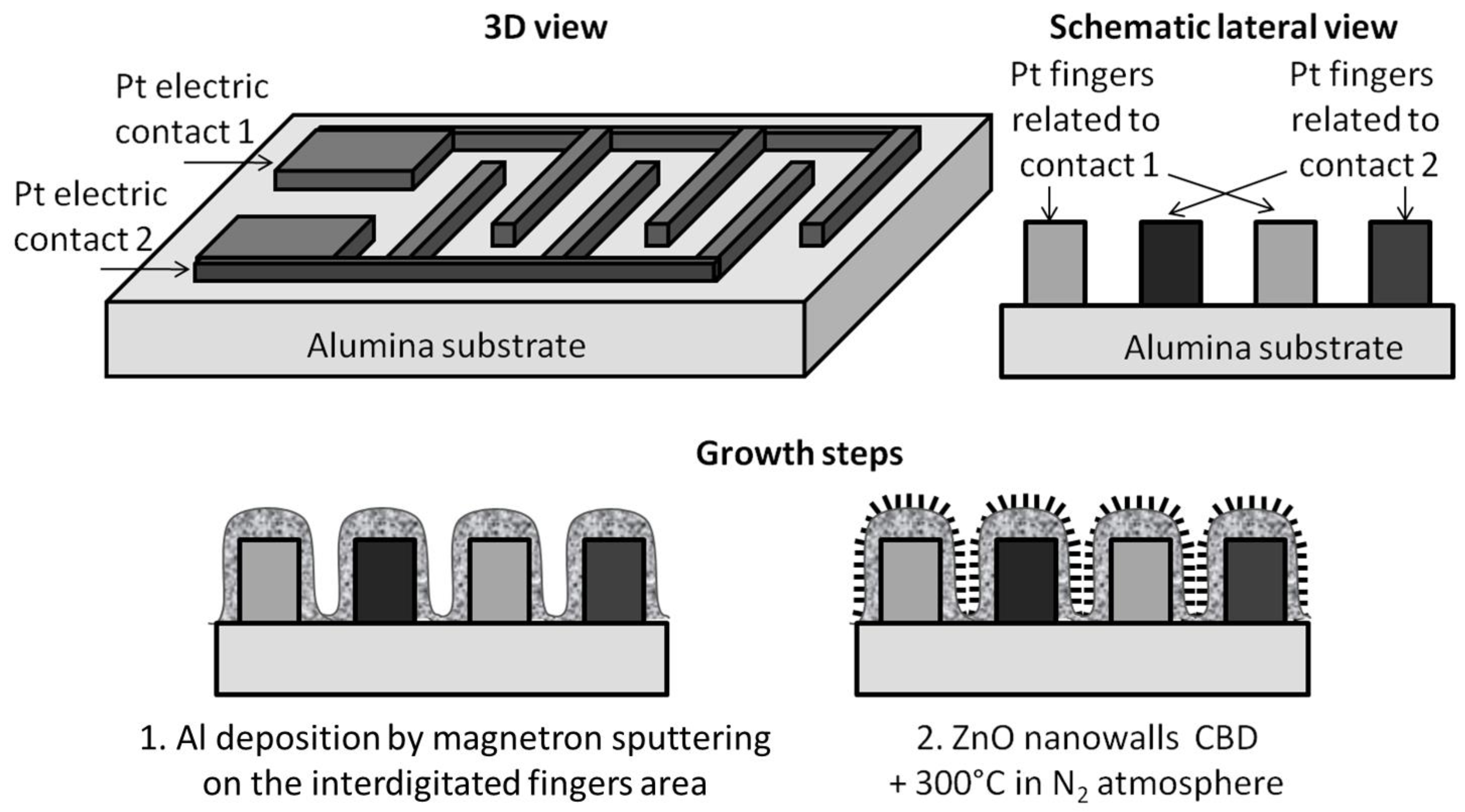
The conductometric sensor was fabricated by using an alumina substrate (6 × 3 mm2), with Pt interdigitated electrodes and a Pt heater located on the backside, as a platform. ZnO nanowalls (NWLs) were grown on the sensing platform by means of chemical bath deposition method. For this scope, a thin layer of aluminum (about 20 nm thick) was first deposited by room temperature sputtering onto the Pt interdigitated electrodes. The device is masked with Kapton tape in order to limit the deposition of aluminum to the Pt fingers area. The base pressure of the deposition chamber was 8 × 10⁻⁶ mbar and the sputtering process was carried with a working pressure of 2.7 × 10⁻³ mbar in argon atmosphere. The pure Al target was pre-sputtered for few minutes in order to remove the surface oxide layer. The Al layer was deposited with a power of 59 W for 3 min. The ZnO growth solution was prepared by mixing in a beaker zinc nitrate hexahydrate (≥99.0%) and hexamethylenetetramine (HMTA, ≥99.5%), in equimolar ratio (25 mM), using 400 mL deionized water (DI, MilliQ, 18.2 MΩ·cm) as solvent. The solution was kept under magnetic stirring for 30 min and then heated at 90 °C in a boiling water bath (bain.marie configuration). The device was then vertically immersed in the beaker, at half height. After 1 h, the sample was extracted from the chemical bath, rinsed with DI water, dried and annealed in inert atmosphere with nitrogen gas for 1 h at the temperature of 300 °C. Finally, the sensor was cooled at room temperature and then stored at ambient conditions before use. A schematic representation of the whole sensor fabrication process is reported in Figure 1.
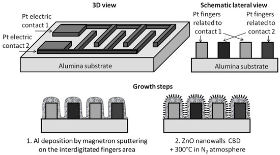
Figure 1.
Schematization of the various steps for the preparation of the ZnO nanowalls-based conductometric sensor.
2.2. Characterization of the Sensing Layer
The morphological and structural properties of ZnO NWLs film were analyzed by scanning electron microscopy (SEM, Gemini 152 field emission SEM Supra 25 , Carl Zeiss, Oberkochen, Germany ) and by the electron beam of a Versa 3D Dual Beam Focused Ion Beam (FEI, Hillsboro, OR, USA) and by X-ray diffraction (XRD, D-500 diffractometer, Bruker, Billerica, MA, USA). Crystallite sizes (d, in nm) were estimated from the Scherrer’s equation:
where λ is the X-ray wavelength, θB is the maximum of the Bragg diffraction peak (in radians) and B is the full width at half maximum (FWHM) of the XRD peak.
2.3. Sensing Tests
Sensing tests were carried out in a stainless-steel test chamber. The experimental bench for the electrical characterization of the sensors allows us to carry out measurements in controlled atmosphere. Gases coming from certified bottles can be further diluted in air at a given concentration by mass flow controllers. Measurements were carried out in the temperature range from room temperature (25 °C) to 400 °C, with steps of 50 °C, under a dry air (RH < 3%) total stream of 100 sccm, collecting the sensors resistance data in the four point mode. An Agilent 34970A (Santa Clara, CA, USA) multimeter was used for this purpose, while a dual-channel power supplier instrument Agilent E3632A was employed to bias the built-in heater of the sensor to perform measurements at super-ambient temperatures. The gas response, S, is defined as S = Rgas/Rair, where Rgas is the electrical resistance of the sensor at different gas concentrations in dry air and Rair the baseline resistance in pure dry air.
3. Results
3.1. Sensing Layer Synthesis and Characterization
First, we attempted to grow the ZnO NWLs on the bare alumina substrate, but this approach failed, confirming that for their formation they need of a thin layer of metallic aluminum, acting as a catalytic layer [8]. Thereby, an Al layer of about 20 nm was deposited by sputtering onto the Pt interdigitated fingers area of the electrodes (but covering the Pt electric contacts). It is noteworthy that such a thin layer is partially oxidized during the CBD, so it will not act as a short circuit between electrodes. During the CBD, the substrate was held vertically (for 1 h @ 90 °C) in the chemical bath (Zinc nitrate + hexamethylenetetramine) solution. After the ZnO NWLs deposition, the substrate was dried and annealed in inert atmosphere for 1 h at the temperature of 300 °C.
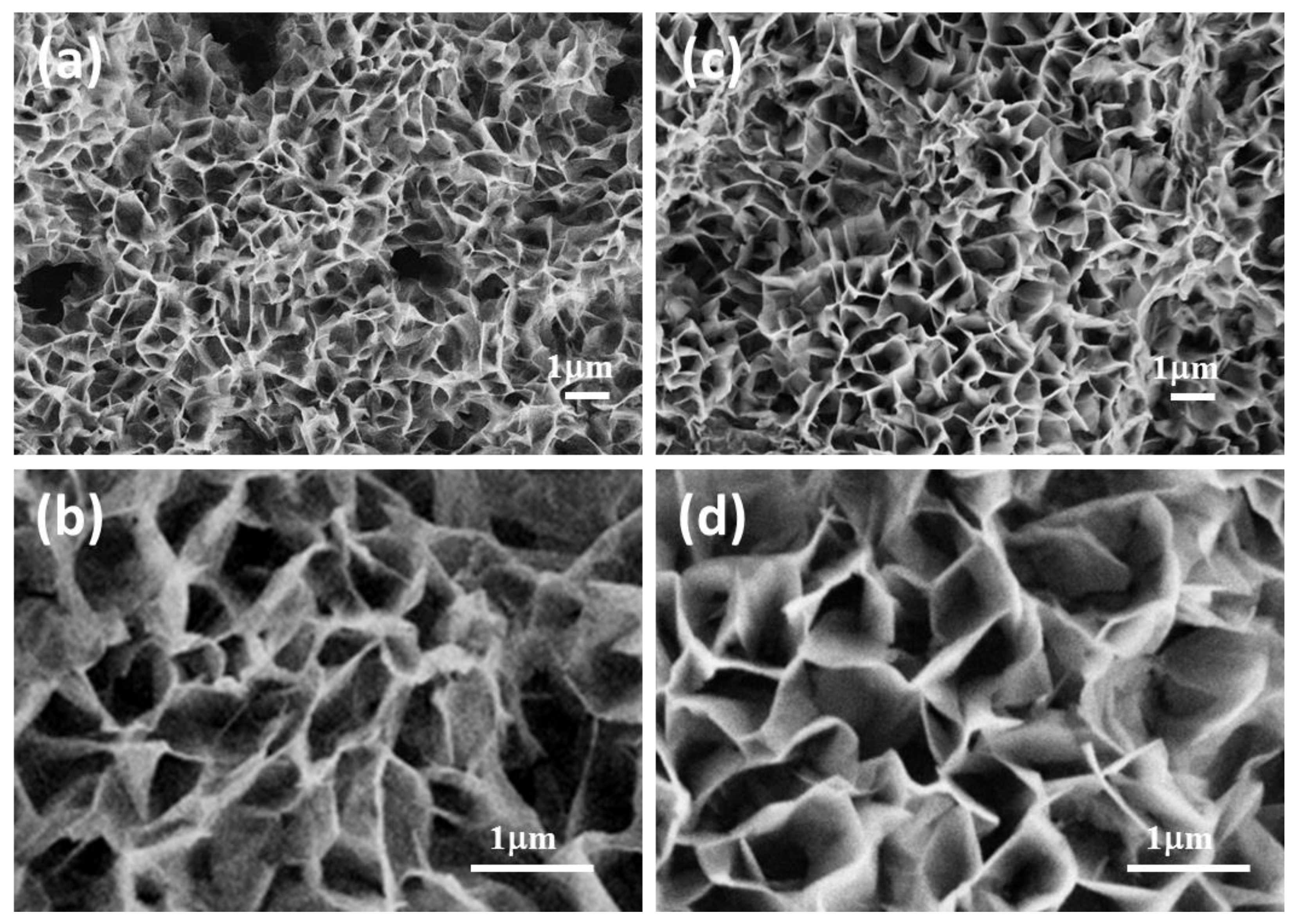
SEM analyses of the as-grown and annealed substrate are provided in Figure 2, showing the morphology of the sensing layer surface. A well-developed network of ZnO NWLs grown on the conductometric platforms is clearly noted. The as grown and annealed films (1.7 µm thick) consist of intertwined 2D foils, vertically grown on the substrate, providing very high surface-to-volume ratio. The annealing treatment does not cause a morphological change of the NWLs.

Figure 2.
Scanning electron microscopy images of (a,b) as grown and (c,d) annealed sensing layer surfaces taken at different magnification.
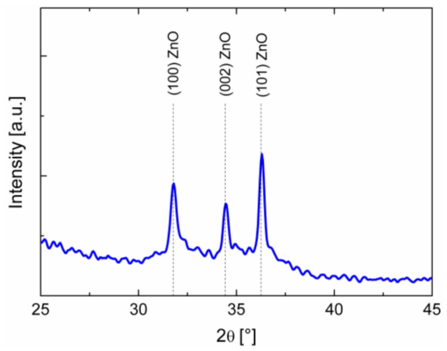
X-ray diffraction analysis of the annealed ZnO NWLs sensing layer is reported in Figure 3. The diffraction pattern confirms the presence of ZnO crystal structure with the typical reflection peaks of ZnO (100, 002, 101). The crystallite dimension was estimated by the X-ray reflection peak broadening method via the Scherrer equation. The crystallite size, calculated assuming a Gaussian-type distribution for each individual peak, varies from 29.3 to 38.6 nm over the diffraction angle range 31.78°–36.27°, with an average value of 34 nm.

Figure 3.
X-ray diffraction analysis of the sensing layer on the annealed sensor.
3.2. Sensing Tests
First, preliminary measurements were carried out to acquire information about the electrical characteristics of the sensor. At room temperature and up to 250 °C, the ZnO nanowalls-based sensor showed very high resistance, out of the range of measurement of our instrumentation. This hindered us from making any measurement in this low temperature range. Above the temperature of 250 °C, the sensor showed a significant decrease of electrical resistance with the increasing of temperature, following the expected behavior for a semiconductor material.
Sensing measurements were then performed at high temperatures, in the range 250–400 °C. To evaluate the gas sensing properties (in terms of sensitivity, response and recovery times, as well as selectivity), the sensor was subjected to repeated pulses of CO and NO2 at low concentrations in synthetic dry air (20% O2 + 80% N2, RH < 3%). It was noted that the sensing properties of the sensor with a layer of ZnO NWLs grown for 1 h @ 90 °C, although very remarkable, are not fully reproducible when we attempted to fabricate different devices in the same above conditions. This suggests that the growth of the 2D-ZnO walls on the sensing area is the critical step of the fabrication process of these sensors and should be optimized in order to obtain more reliable devices.
Further, in its initial state, the sensors present a p-type behavior, as demonstrated by the increase of the resistance on addition of carbon monoxide. Such a finding can be explained by nitrogen doping of the ZnO NWLs. In this hypothesis, nitrogen would adsorb at the grain boundaries during the growth/annealing steps and act as an electron trap, thus favoring the p-type semiconducting behavior [17]. However, the initial p-type behavior of the ZnO NWLs network evolved and stabilizes into n-type one. This mechanism change involved also a decrease of the sensor response. The sensor characteristics modification observed can be related to the change of surface defects. In any case, after that, the sensors appear stable and reproducible.
The loss of p-type properties after annealing treatment in air toward n-type behavior has been well documented in the literature [18]. Regarding the subsequent annealing in air, as a consequence, we noted also the strong decline/modification of the gas sensing properties of ZnO NWLs. On the basis of these observations, our suggestion is that the response decline is linked to the reduction of the reactive oxygen defects concentration. The role of humidity adsorbed in changing the sensor characteristics is also of utmost importance and should be investigated more in detail.
A detailed characterization of the sensing layer is under progress to reveal the key factors responsible of the above transition behavior. This is most important not only to acquire helpful information for clarifying the sensing mechanism, but also from a practical point of view. Indeed, considering the very high sensitivity observed initially, a “freezing” of the initial sensor characteristics could allow us to maintain very high performance and this is our next objective.
On the other hand, it is worth noting that, when increasing the growth time (from 1 to 2 h @ 90 °C) of ZnO nanowalls, the fabricated sensors also had a more reproducible sensing behavior and were much more stable. In addition, as for the 1 h samples annealed, its semiconducting behavior with respect to carbon monoxide is changed. Indeed, a resistance decrease in the presence of CO has been noted owing to their initial use. We can attribute this to a lower number of oxygen vacancies in the ZnO NWLs sensing layer grown for longer time, and a diminution of N doping.
To explain this behavior, we should note that, in air, oxygen adsorbs on the surface of the ZnO NWLs to form oxygen ions. On exposure to carbon monoxide at the operating temperature of 350–400 °C, O2− species are expected to interact with CO coming from the gas phase:
CO(g) + O2−(ads) → CO2 + 2e−
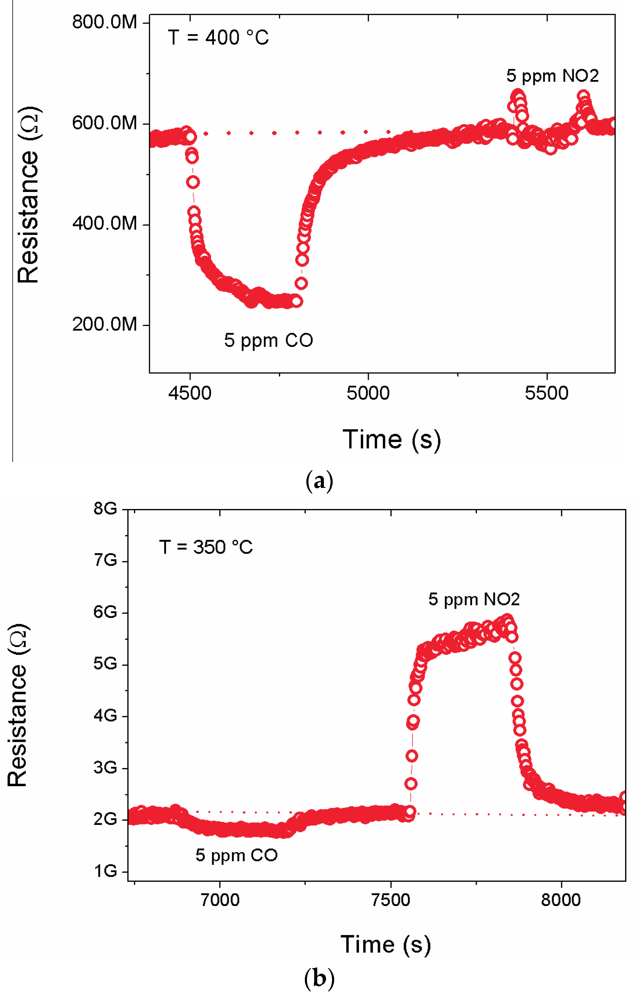
This causes the release of electrons in the bulk, resulting in a decrease of the resistance, as expected for n-type semiconductor, as reported in Figure 4 for the sample grown for 1 h and annealed.

Figure 4.
Variation of resistance to pulses of CO and NO2 at two different temperatures, under a dry air (RH < 3%) flow.
Regarding NO2 sensing tests, at the higher temperature (400 °C), no clear response was observed. Decreasing the temperature to 350 °C, the sensor resistance increased. The behavior registered in the presence of NO2 can be explained taking into account the complex interaction of nitrogen dioxide with the surface of many semiconducting metal oxides, resulting in a non-linear behavior depending on the temperature and NO2 concentration [19,20].
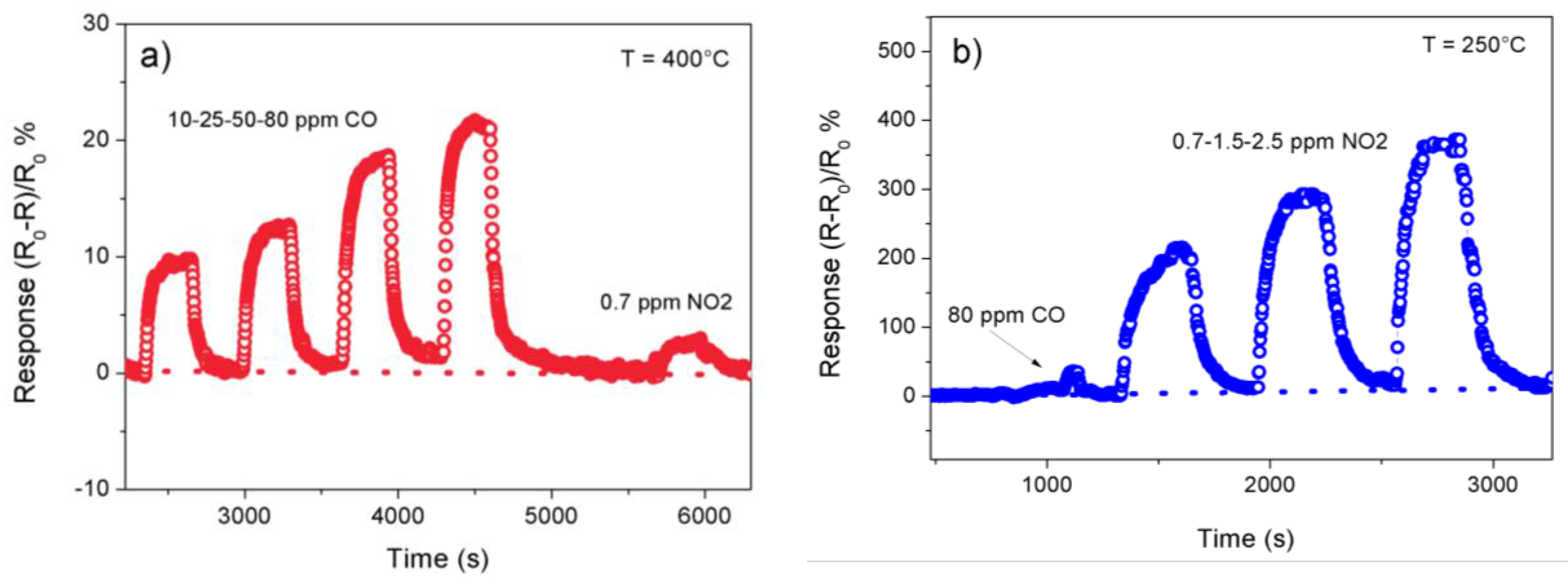
The above results indicated that the sensor performance is highly dependent on the operating temperature. Interestingly, when properly choosing the operating temperature, the sensor demonstrated the opposite response to CO and NO2, respectively. The ability to distinguish between NO2 and CO when employing low and high operation temperatures is due to the well-known bell-shaped response curves of metal oxide gas sensors [21] and the commonly lower detection temperatures for the case of NO2. Therefore, we tested the sensor at two different temperatures, chosen for maximizing the sensitivity and selectivity toward CO and NO2. The dynamics of the responses obtained are shown in Figure 5. At the temperature of 400 °C, the sensor responded selectively to CO, being almost insensitive to the low concentration of NO2 (Figure 5a). At the lower temperature of 250 °C, the sensor was instead very sensitive and selective to NO2 (Figure 5b).
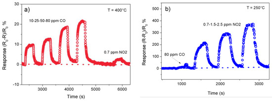
Figure 5.
Dynamics of the response of the sensor to (a) CO and (b) NO2, at two different temperatures, under a dry air (RH < 3%) flow.
The calibration curves, related to the above experiments, are reported in Figure 6a,b. It is clearly observed that, at higher temperature, the sensor responds selectively to CO, whereas at a lower temperature the sensor is instead very sensitive and selective to NO2 (see insets in Figure 6a,b).
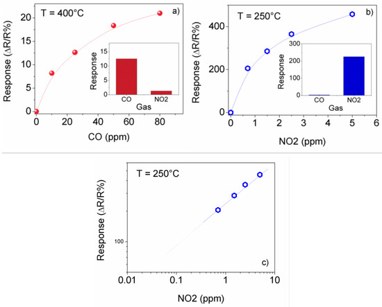
Figure 6.
Calibration curves for (a) CO and (b) NO2. In the insets are shown the response to CO (25 ppm) and NO2 (0.75 ppm). (c) Log-log plot of the NO2 calibration extrapolated to low concentration levels.
A lower detection limit (LOD) of about 50 ppb (at S/N = 3), which accomplishes the requirement for environmental monitoring, has been estimated as evinced by the calibration plot reported in Figure 6c. These sensing characteristics qualified them as comparable to state-of-the-art conductometric ZnO sensors [22,23,24].
4. Conclusions
In this paper, we demonstrated the interesting sensing characteristics toward CO and NO2 of ZnO nanowalls grown on conductometric platforms. By the simple chemical bath deposition method used, we were able to grow these nanostructures on the Pt interdigitated electrodes area of conductometric alumina platforms. The sensor response to CO or NO2 was found to be strongly dependent on the operating temperature, allowing us to tailor the selectivity toward the desired target gases. Some hypotheses have been formulated to take into account the sensor performances. It was also verified that the growth time of ZnO nanowalls has a strong impact on the sensing performances, suggesting that short growth times may favor the formation of many O vacancy defects and/or nitrogen doping at grain boundaries with respect to long ones, affecting the adsorption behavior of gas molecules on metal oxide surfaces and consequently their sensing properties. A deeper microstructural characterization, electrical and sensing investigation is in progress in order to better understand the sensing mechanism(s) involved and clarify the origin of the results obtained. Tests with other gases like humidity, methane, ethanol and ammonia have been also planned in future investigations.
Acknowledgments
We acknowledge Giacomo Torrisi (University of Catania, Italy) for the Al sputtering and C. Percolla e G. Pantè (IMM-CNR) for their technical support. This work has been performed within the framework of the PON project Bio-nanotech Research and Innovation Tower (BRIT), financed by the Italian Ministry for Education, University and Research (MIUR) (Grant no. PONa3_00136).
Author Contributions
E.B. and V.S. synthesized the ZnO NWLs on the interdigitated electrodes; E.B., V.S. and S.M. performed the structural analysis; N.D. and S.G.L. performed the electrical and sensing tests. All the Authors contributed to idea conceivement and paper writing.
Conflicts of Interest
The authors declare no conflict of interest.
References
- Neri, G. First fifty years of chemoresistive gas sensors. Chemosensors 2015, 3, 1–20. [Google Scholar] [CrossRef]
- Ye, C.; Bando, Y.; Shen, G.; Golberg, D. Thickness-dependent photocatalytic performance of ZnO nanoplatelets. J. Phys. Chem. B 2006, 110, 15146–15151. [Google Scholar] [CrossRef] [PubMed]
- Wang, X.; Ding, Y.; Li, Z.; Song, J.; Wang, Z.L. Single-crystal mesoporous ZnO thin films composed of nanowalls. J. Phys. Chem. C 2009, 113, 1791–1794. [Google Scholar] [CrossRef]
- Maeng, J.; Jo, G.; Choe, M.; Park, W.; Kwon, M.-K.; Park, S.-J.; Lee, T. Structural and photoluminescence characterization of ZnO nanowalls grown by metal organic chemical vapor deposition. Thin Solid Films 2009, 518, 865–869. [Google Scholar] [CrossRef]
- Cheng, J.P.; Zhang, X.B.; Luo, Z.Q. Oriented growth of ZnO nanostructures on Si and Al substrates. Surf. Coat. Technol. 2008, 202, 4681–4686. [Google Scholar] [CrossRef]
- Yao, L.; Zheng, M.; Li, C.; Ma, L.; Shen, W. Facile synthesis of superhydrophobic surface of ZnO nanoflakes: Chemical coating and UV-induced wettability conversion. Nanoscale Res. Lett. 2012, 7, 216. [Google Scholar] [PubMed]
- Gao, S.Y.; Li, H.D.; Yuan, J.J.; Li, Y.A.; Yang, X.X.; Liu, J.W. ZnO nanorods/plates on Si substrate grown by low-temperature hydrothermal reaction. Appl. Surf. Sci. 2010, 256, 2781–2785. [Google Scholar] [CrossRef]
- Iwu, K.O.; Strano, V.; Di Mauro, A.; Impellizzeri, G.; Mirabella, S. Enhanced quality, growth kinetics, and photocatalysis of ZnO nanowalls prepared by chemical bath deposition. Cryst. Growth Des. 2015, 15, 4206–4212. [Google Scholar] [CrossRef]
- Maiolo, L.; Mirabella, S.; Maita, F.; Alberti, A.; Minotti, A.; Strano, V.; Pecora, A.; Shacham-Diamand, Y.; Fortunato, G. Flexible pH sensors based on polysilicon thin film transistors and ZnO nanowalls. Appl. Phys. Lett. 2014, 105, 093501. [Google Scholar] [CrossRef]
- Yu, L.-M.; Guo, F.; Liu, Z.-Y.; Liu, S.; Yang, B.; Yin, M.-L.; Fan, X.-H. Facile synthesis of three dimensional porous ZnO films with mesoporous walls and gas sensing properties. Mater. Charact. 2016, 112, 224–228. [Google Scholar] [CrossRef]
- Yu, L.; Guo, F.; Liu, S.; Yang, B.; Jiang, Y.; Qi, L.; Fan, X. Both oxygen vacancies defects and porosity facilitated NO2 gas sensing response in 2D ZnO nanowalls at room temperature. J. Alloys Compd. 2016, 682, 352–356. [Google Scholar] [CrossRef]
- Chang, S.-P.; Wen, C.-H.; Chang, S.-J. Two-dimensional ZnO nanowalls for gas sensor and photoelectrochemical applications. Electron. Mater. Lett. 2014, 10, 693–697. [Google Scholar] [CrossRef]
- Chen, T.P.; Chang, S.P.; Chang, S.J. Fabrication of ZnO nanowall-based hydrogen gas nanosensor. Adv. Mater. Res. 2013, 684, 21–25. [Google Scholar] [CrossRef]
- Chen, T.-P.; Chang, S.-P.; Hung, F.-Y.; Chang, S.-J.; Hu, Z.-S.; Chen, K.-J. Simple fabrication process for 2D ZnO nanowalls and their potential application as a methane sensor. Sensors 2013, 13, 3941. [Google Scholar] [CrossRef] [PubMed]
- Hjiri, M.; El Mir, L.; Leonardi, S.G.; Donato, N.; Neri, G. CO and NO2 selective monitoring by ZnO-based sensors. Nanomaterials 2013, 3, 357–369. [Google Scholar] [CrossRef] [PubMed]
- Rai, P.; Raj, S.; Ko, K.-J.; Park, K.-K.; Yu, Y.-T. Synthesis of flower-like ZnO microstructures for gas sensor applications. Sens. Actuators B Chem. 2013, 178, 107–112. [Google Scholar] [CrossRef]
- Major, S.; Banerjee, A.; Chopra, K.L. Annealing studies of undoped and indium-doped films of zinc oxide. Thin Solid Films 1984, 122, 31–43. [Google Scholar] [CrossRef]
- Kobrinsky, V.; Fradkin, E.; Lumelsky, V.; Rothschild, A.; Komem, Y.; Lifshitz, Y. Tunable gas sensing properties of p- and n-doped ZnO thin films. Sens. Actuators B 2010, 148, 379–387. [Google Scholar] [CrossRef]
- Dai, Z.; Lee, C.-S.; Tian, Y.; Kim, I.-D.; Lee, J.-H. Highly reversible switching from P- to N-type NO2 sensing in a monolayer Fe2O3 inverse opal film and the associated P–N transition phase diagram. J. Mater. Chem. A 2015, 3, 3372–3381. [Google Scholar] [CrossRef]
- Wang, J.X.; Sun, X.W.; Yang, Y.; Wu, C.M. N–P transition sensing behaviors of ZnO nanotubes exposed to NO2 gas. Nanotechnology 2009, 20, 465501. [Google Scholar] [CrossRef] [PubMed]
- Ahlers, S.; Müller, G.; Doll, T. A rate equation approach to the gas sensitivity of thin film metal oxide materials. Sens. Actuators B 2005, 107, 587–599. [Google Scholar] [CrossRef]
- Shishiyanu, S.T.; Shishiyanu, T.S.; Lupan, O. Sensing characteristics of tin-doped ZnO thin films as NO2 gas sensor. Sens. Actuators B Chem. 2005, 107, 379–386. [Google Scholar] [CrossRef]
- Lupan, O.; Shishiyanu, S.; Chow, L.; Shishiyanu, T. Nanostructured zinc oxide gas sensors by successive ionic layer adsorption and reaction method and rapid photothermal processing. Thin Solid Films 2008, 516, 3338–3345. [Google Scholar] [CrossRef]
- Dinesh, V.P.; Sukhananazerin, A.; Biji, P. An emphatic study on role of spill-over sensitization and surface defects on NO2 gas sensor properties of ultralong ZnO@Au heterojunction NRs. J. Alloys Compd. 2017, 712, 811–821. [Google Scholar] [CrossRef]
© 2017 by the authors. Licensee MDPI, Basel, Switzerland. This article is an open access article distributed under the terms and conditions of the Creative Commons Attribution (CC BY) license (http://creativecommons.org/licenses/by/4.0/).

