Abstract
Since the first report of graphene, thin two-dimensional (2D) nanomaterials with atomic or molecular thicknesses have attracted great research interest for gas sensing applications. This was due to the distinctive physical, chemical, and electronic properties related to their ultrathin thickness, which positively affect the gas sensing performances. This feature article discusses the latest developments in this field, focusing on the properties, preparation, and sensing applications of thin 2D inorganic nanomaterials such as single- or few-layer layered double hydroxides/transition metal oxides/transition metal dichalcogenides. Recent studies have shown that thin 2D inorganic nanomaterials could provide monitoring of harmful/toxic gases with high sensitivity and a low concentration detection limit by means of conductometric sensors operating at relatively low working temperatures. Promisingly, by using these thin 2D inorganic nanomaterials, it may open a simple way of improving the sensing capabilities of conductometric gas sensors.
1. Introduction
Materials with thin 2D morphologies comprise a large family of organic and inorganic compounds, as well as organic/inorganic hybrid composites, with the common characteristic of presenting a very high area to thickness ratio. Because of their unique structural features and outstanding properties, thin 2D nanomaterials have become a key class of materials in chemistry, physics, and materials science, and have been extensively investigated for their promising applications in different fields [1]. In recent years, thin 2D semiconductors with controllable band gaps and doping have been exploited in optoelectronic devices such as photodiodes, solar cells, and light-emitting diodes [2].
Thin 2D nanomaterials have unique characteristics that make them different from other types of nanomaterials with different dimensionalities such as zero-dimensional (0D) nanoparticles, one-dimensional (1D) nanowires, and three-dimensional (3D) networks. Furthermore, compared to bulk 2D materials, they offer large lateral size and ultrathin thickness, which endow them with an ultrahigh specific surface area, offering an extremely large proportion of surface atoms. For example, five-atomic-layer-thick 0.66 nm SnO2 sheets have 40% surface atom occupancy by highly reactive surface Sn and O atoms with low coordination numbers [3]. These surface atoms could serve as adsorption centers to efficiently adsorb gaseous molecules and/or catalytically active sites, favoring the surface reactions of adsorbed species.
In addition, the electron confinement in two dimensions of ultrathin 2D nanomaterials, especially single-layer nanosheets where interlayer interactions are absent or limited, enables greatly compelling electrical properties compared to other nanomaterials. Furthermore, as they encompass a wide range of elemental compositions that give rise to properties spanning metallic, semiconducting, and insulation behaviors, fine tuning can be attempted to improve their electrical characteristics. These properties are highly favorable for gas sensing applications. It is well known that environmental conditions, such as the presence of reactive chemical species and water molecules, can affect the electrical properties of thin 2D sheets [4]. These features have then been exploited to extend their applications to gas sensing technologies.
Monolayer graphene sheets are likely the most known and investigated thin 2D nanomaterial since Novoselov’s success in exfoliating graphite in 2004 [5]. After this achievement, there has been an increase in the preparation of other thin two-dimensional inorganic materials. At present, many thin 2D inorganic nanomaterials are well known and very excellent reviews have appeared in the recent literature to cover all aspects regarding these materials [6,7].
In this feature paper, our attention is focused on the gas sensing properties of inorganic thin 2D-sheets. A brief overview and discussion of the recent progress on the development of these nanostructures, rather than offering a comprehensive review, is presented. The more representative classes of inorganic materials with graphene 2D sheet morphology are shown in Figure 1. Thin 2D metal oxides (MOX), transition metal dichalcogenides (TMDs), transition metal carbides/nitrides (Mxenes), elemental analogues of graphene (silicene, phosphorene, and borophene), and other 2D structures such as h-BN, represent a very important sub-class of the general two dimensional materials [8]. A review of the literature revealed that Layered Double Hydroxides (LDHs), Metal Oxides (MOX), and Transition-Metal Dichalcogenides (TMDs) are the classes mainly used for gas sensing applications (see the outer-sphere of the picture shown in Figure 1).
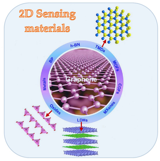
Figure 1.
Representative classes of graphene-like inorganic materials. The layer structure of three classes mainly used for gas sensing applications (i.e., Layered Double Hydroxides (LDHs), Metal oxides (MOX), and Transition-metal dichalcogenides (TMDs)) are indicated by the red arrows. Reproduced with permission from ref. [8].
Layered Double Hydroxides (LDHs)—LDHs are a class of two-dimensional layered inorganic matrices structurally conformed by a consecutive repetition of individual sheets located in parallel spatial planes, that are electrostatically bonded by Van der Waals interactions or hydrogen bonds along the perpendicular plane [9]. LDHs contains anions (e.g., CO32−, Cl−, etc.), intercalated between positive layers, which significantly affect their structure and d-spacing. By varying the metallic cations, their ratio, and the interlayer anions, a great number of LDHs types can be formed. LDHs structure exhibits a pathway facilitating carrier diffusion/transportation, therefore they received considerable attention for direct potential applications in gas sensors for monitoring a wide class of gases and vapors such as nitrogen oxides, acetone, and ethanol [10]. 2D layered materials have been also used as precursors for obtaining thin two-dimensional metal oxides [11,12,13].
Metal oxides (MOX)—Over the past five decades, gas sensors based on semiconducting metal oxides have drawn much attention [14]. Initially, three dimensional materials were used, which were later replaced by two dimensional materials because of their superior gas sensing performances. Nevertheless, thin 2D MOX show more favorable sensing properties, maintaining the proper considerable advantages of metal oxide materials, mainly: (i) good thermal and chemical stability; (ii) tunable electrical properties; (iii) possibility of doping the bulk/surface with elements acting as structural or catalyst promoters [15].
Transition-metal dichalcogenides (TMDs)—TMDs are inorganic compounds that have a general formula MX2, where M represents a transition metal element from group 4 to group 10, and X represents a chalcogen element (S, Se, and Te). These materials, when reduced in the form of single- or a few-layers, offer excellent electronic performance which is comparable to that of graphene [16]. In addition, unlike graphene, they display a bandgap sufficient for practical device applications [17]. Several 2D-TMDs possess sizable band-gaps around 1–2 eV, which is due to their low intrinsic carrier concentration. This allows them to operate at much higher temperatures than graphene, on the order of 300 °C, which is attractive for modulating their transport characteristics and enhancing their sensing performances. Among this vast class of materials, disulfides such as MoS2, WS2, and SnS2, surely represent the most investigated materials for gas sensing [18].
Studies on these nanostructures are actually growing at a very high rate and then regularly updating the reported work in this emerging research area is of the outmost importance in order to follow the most recent progress and obtain an indication for future research. Therefore, in this feature paper we first discuss the main factors contributing to the gas sensing performances of thin 2D nanomaterials and then report on the more recent developments in this field.
2. Factors Influencing the Gas Sensing Characteristics of Thin 2D Nanostructures
In gas sensing applications, dimensionality of the nanostructure undoubtedly plays a key role for efficient monitoring. Many factors associated with the general characteristics of thin 2D nanostructures are responsible for this. The ultrahigh thickness and its very high associated surface area is one of the most important factors that helps to enhance the gas sensing performance of thin 2D nanostructures (Figure 2).
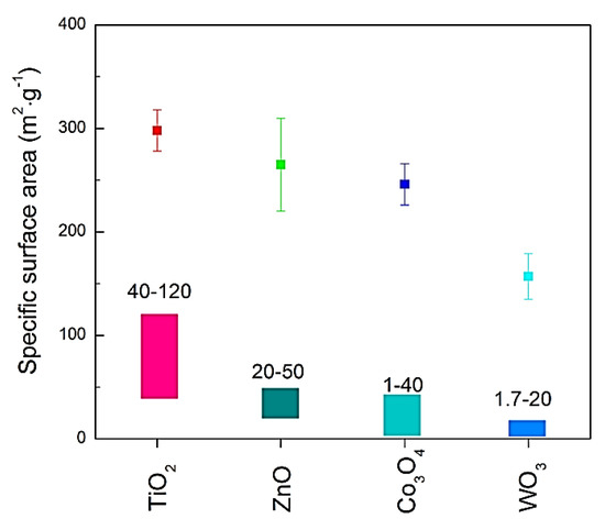
Figure 2.
Specific surface areas of 2D metal oxide nanosheets. Specific surface areas of the 2D metal oxide nanosheets (individual symbols with error bars) together with the reported specific surface areas (individual bars with numbers) of the conventional metal oxide nanoparticles. Reprinted with permission from ref. [15].
The high surface area makes them highly sensitive to the adsorption of gaseous molecules on the surface [15]. In the case of monolayer 2D nanostructures, the whole surface is theoretically exposed to the gas influence and is potentially promising for ultra-high sensitivities. Furthermore, on their surfaces, the atoms are unsaturated due to the lower coordination number. Because the adsorption of gaseous species on solid surfaces usually occurs on the low coordinated steps, edges, terraces, kinks, and corner atoms, the number of chemisorbed gaseous molecules will be high. In the atomically-thin two-dimensional sheets, owing to their high fraction of these sites with highly reactive sites, an improvement of the sensing performance can be expected with respect to their higher dimensional material counterparts [19].
The sensing properties of thin 2D-sheets of inorganic materials derive also from their unique electronic structures [20]. It is expected that the electrical properties of these materials differ substantially from that of their bulk counterparts. The essential factors of a material for gas sensing applications include high charge carrier mobility, high conductivity, and a suitable band gap energy. Compared to graphene, which has high charge carrier mobility and conductivity but presents some limitations because of the lack of an intrinsic band gap, thin 2D inorganic layered materials appear to be the most promising due to an appropriate band gap (Figure 3).
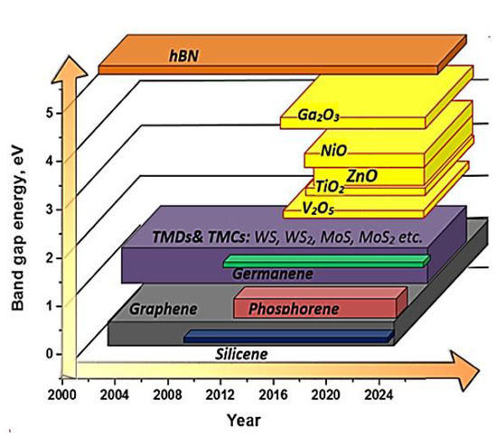
Figure 3.
Intrinsic band gap of graphene-like thin 2D inorganic layered materials. Comparing all these 2D materials, it can be noted that graphene is characterized by zero intrinsic band gap energy, whereas regarding the other thin 2D inorganic layered materials of interest for gas sensing (TMDs and MOX), they exhibit an increasing band gap going from TDMs to MOX. Reprinted with permission from ref. [20].
Interestingly, the band gap can be modulated by tuning the layer numbers. As an example, referring to bulk and few- to mono-layer MoS2, a group 6 TMDs with a trigonal prismatic structure, the bulk material is an indirect-gap semiconductor having a bandgap of ~1 eV. In contrast, an isolated monolayer of the same material is a direct-gap semiconductor. In addition, there is an indirect-to-direct bandgap transition going from a bulk to a monolayer material which arises from quantum confinement effects, as probed by high photoluminescence in the monolayers of MoS2, whereas only a weak emission is observed in the multilayered form. In general, in the case of group 6 TMDs, the monolayer bandgap is typically ~50% larger than that of the bulk materials [21]. Thus, the electrical characteristics of practical gas conductometric sensors can be tuned up by the appropriate modulation of the number/thickness of the two-dimensional sensing layer.
Furthermore, by examining the electronic structures of such thin 2D materials, such as the density of states (DOS), important information can be acquired which is essential to understand their intrinsic charge transporting characteristics. It has been demonstrated that changes in interlayer coupling, the degree of quantum confinement, and symmetry elements lead to dramatic differences in the electronic structure of single-layer materials, i.e., increases at the valence band edge with respect to the bulk material [22]. The electronic structure of single-layer material is furthermore strongly influenced by adsorbed species. Figure 4 shows the density of states in MoS2 thin 2D sheets which significantly undergo substantial changes after O2 adsorption on the Mo–S bridge sites. Of course, this aspect is of crucial importance for the sensing characteristics of thin 2D inorganic materials.
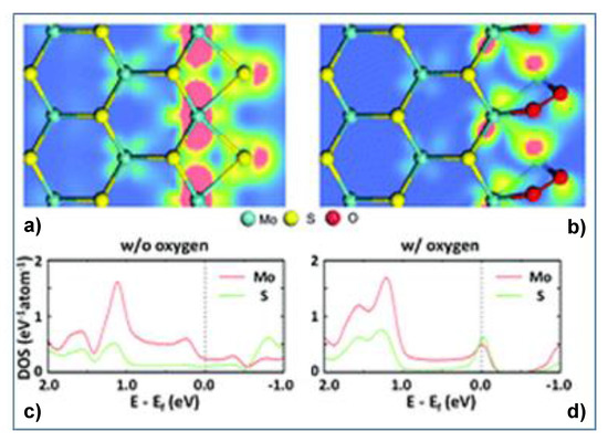
Figure 4.
Charge density distribution near the Fermi level (a,b) and density of states (c,d) of clean Mo-edges with S monomers and O2 adsorbed Mo-edges with S monomers on the Mo–S bridge site. The red and blue colors in the charge density distribution indicate the maximum and zero electronic densities, respectively. Reprinted with permission from ref. [22].
Electron confinement in two-dimensions also deeply affects the performance of gas sensors [23]. 2D-based sensors exhibit strong thickness dependence, with a remarkable enhancement in the sensor response as the thickness is reduced into the regime of quantum confinement. The thickness scaling trend has been attributed to the quantization of electrons which favorably alters both the position, moving the charge center closer to the top surface, and the transport properties of charge carriers, mainly due to the reduced density of states (DOS) for 2-D semiconductors, thus making them more susceptible to surface phenomena.
Despite the extensive theoretical and experimental work performed for understanding the structure and properties of these unique thin 2D nanomaterials, the influence of the shape on the mechanism of gas sensing via the adsorption/desorption/reaction of gas molecules on the surface are not yet well understood. The sensing mechanism of conductive sensors relies on the charge transfer which occurs between the sensing layer and surface chemisorbed species. Such a charge transfer affects the electrical resistance of the sensitive material, representing the response of the sensor [14]. Generally, for LHDs or MOX chemoresistive sensors, the presence of oxygen is crucial for this mechanism, because electron transfer occurs through chemisorption of the oxygen reactive species O2−, O−, O2−, which react with the chemisorbed target gases [24]. Obviously, high operation temperatures (usually above 200 °C) are needed to obtain this.
The sensing mechanism of TMDs layered nanomaterials is instead typically based on physisorption-charge transfer processes [25]. Physical adsorption dominates at relatively low operating temperatures, so this approach is an advantage for minimizing power consumption of sensors and increasing their life-time [26]. Based on the physisorption-based charge transfer, Ou et al. integrated 2D SnS2 flakes onto low-cost resistive transducing platforms for highly selective and exceptionally sensitive NO2 gas sensing at ppb levels [27]. Interestingly, this aspect has further advantages related to the selectivity of sensors based on this gas sensing mechanism principle. Indeed, in agreement with the theoretical calculations of the binding energies, which indicate that NO2 is the most strongly bound species with respect to the other species tested, sensing tests confirmed the high selectivity toward this gaseous species (Figure 5).
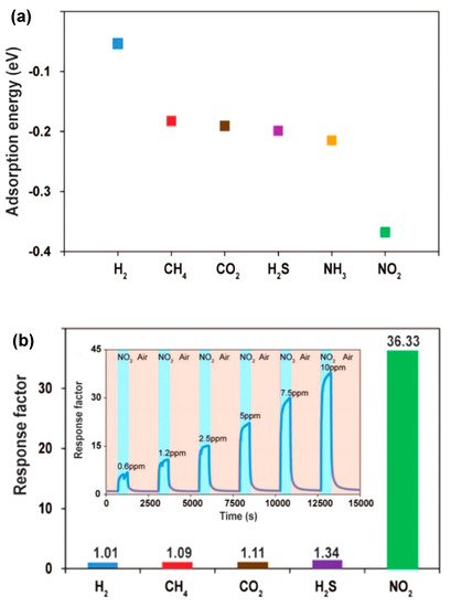
Figure 5.
Gas-sensing performance of 2D SnS2 flakes. (a) Calculated molecule surface adsorption energies of 2D SnS2 flakes toward the aforementioned gases together with NH3. (b) Measured cross-talk of 2D SnS2 flakes toward H2 (1%), CH4 (10%), CO2 (10%), H2S (56 ppm), and NO2 (10 ppm). Inset shows the dynamic sensing performance of 2D SnS2 flakes toward NO2 gas at concentrations ranging from 0.6 to 10 ppm under the operation temperature of 120 °C. Reprinted with permission from ref. [27].
3. Synthesis Methods of Thin 2D Inorganic Materials
The preparation of thin 2D materials is one important step in the development of gas sensing devices. In this paragraph, only a brief examination of the most representative procedures for synthesizing thin 2D inorganic materials is reported. The reader is therefore directed to many reviews covering this aspect [28,29]. To date, anisotropic layered bulk materials have been regarded as the most effective precursors for fabricating thin 2D sheets, owing to the weak van der Waals interaction between the layers [30]. The atomically thin layered materials can be isolated from strongly anisotropic bulk materials, such as TMDs, consisting of in-plane covalently bonded atomic layers that interact only weakly with other constituents in the out-of-plane direction. In practice, in order to obtain 2D-nanosheets a number of different techniques and methods have been reported [29]. The picture shown in Figure 6 summarizes the main synthetic processes used for the preparation of 2D layered inorganic nanomaterials.
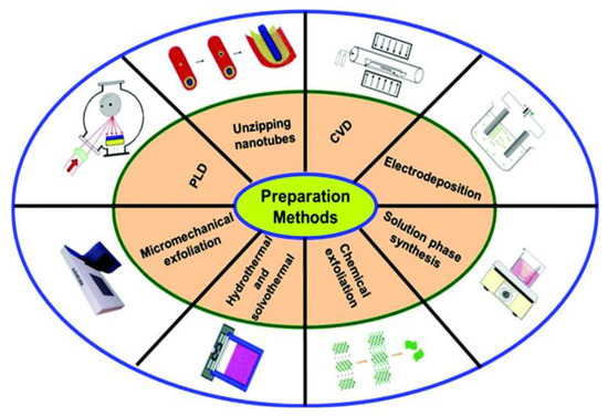
Figure 6.
Main synthetic approaches used to fabricate 2D layered inorganic nanomaterials. From ref. [28].
Among these, mechanical processes use mechanical mechanisms to carry out the exfoliation of the starting layered precursors, such as ultrasonic methods, stirring, freeze-drying, or centrifugation systems [31,32,33]. Historically, this was a key step in the synthesis of graphene-like materials as single-layer graphene sheets were first obtained successfully by Novoselov in 2004 [5].
Wet chemical processes comprise the synthesis by the solvation of interlayered cations or molecules intercalation in the interlayered space (see Figure 7, representing a typical flow process for this method), which facilitates the separation between the layers due to the decrease of the attraction forces and/or increasing the separation between the inorganic layers favoring their random spatial disorder [34,35,36].
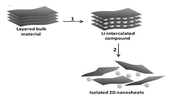
Figure 7.
Lithiation process for the fabrication of 2D nanosheets from the layered bulk material. Adapted from ref. [36].
Most importantly, the synthesis processes should allow for the control of the final properties exhibited by the thin 2D material, preserving the crystalline structure of each individual inorganic layer, with a controllable number of atomic layers and atomically sharp interfaces [37]. This aspect is necessary for ensuring the device reliability requested for practical applications. For commercialization, scalable, low-cost, high yield production of thin 2D materials and compatibility with conventional semiconductor fabrication processes are essential. For this reason, it is imperative to move beyond the mechanical techniques. On the other hand, in liquid exfoliated materials, residual solvents and impurity contamination can deteriorate the electrical performance. In certain cases, chemical and physical vapor deposition (CVD, PVD) of thin 2D materials are considered the methods of choice for the synthesis of high quality films, on a large scale, and in a reproducible manner [38].
4. Gas Sensing Properties of Thin 2D Inorganic Materials
Solid state gas sensors show several practical advantages such as small size and low cost compared to traditional analytical techniques for gas monitoring. Gas sensors based on electrical transduction systems, in which the electrical properties of the sensing layer change with the concentration of the gas surrounding the sensor, have been the most largely investigated. Among these, conductometric (resistive) sensors display interesting features such as miniaturization capability and the unique ability to detect very low concentrations (ppb levels) of gaseous species. A lot of excellent books/reviews on conductometric sensors have been published; the reader is referred to those cited in the review reported in ref. [14]. The sensing mechanism of conductometric gas sensors relies on the change in resistance after the interaction and charge-transfer of the gas target with the surface of the sensitive layer [39]. In the case of gas sensors based on a thin 2D sensitive layer, the ultrathin thickness affords a direct conduction pathway, which can make electron transport more effective; then, the few charges acquired from surface reactions will cause large changes of conductivity of the whole structure, so these sensors are highly sensitive to the gas molecules.
In the following we report and discuss relevant up-to-date examples of gas sensors based on the above cited categories of thin 2D inorganic materials.
4.1. LHDs Sheets
Thin layered double hydroxides display large potential in the gas sensing area due to the facile tunability of their composition, structure, and morphology. However, even if their characteristics make them very good candidates for gas sensing, LDHs have not yet been deeply investigated in this direction. Zn/Al-LDHs materials have been prepared and tested in various atmospheres by Polese and coworkers. The results show that this kind of material is able to detect the tested volatile compounds (CH4, CO, NO) and discriminate different concentrations at room temperature [10].
More often LDHs are instead used as a source precursor for gas sensing materials; the resulting metal oxides can be obtained by roasting the layered nanosheets, showing high stability against sintering, homogeneous dispersion between the elements, and contributing to better gas sensing properties [40]. Metal oxide nanosheets (such as Ti−δO2, Ti1−xCoxO2, MnO2, and perovskites) were synthesized by delaminating appropriate layered precursors into their molecular single sheets via a soft-chemical process [41,42].
4.2. Thin 2D Metal Oxides
Metal oxides such as ZnO, SnO2, TiO2, In2O3, WO3, Fe2O3, and MoO3 have been investigated for a long time in the development of conductometric gas sensors [43]. Their low cost, easy production, chemical stability, and suitable electrical properties played a key role in the commercialization of MOX devices, in particular those based on SnO2 and ZnO in the past fifty years [14]. Among the various typology of MOX with different dimensionalities, thin 2D metal oxide nanosheets now have relevant importance for exploiting novel gas sensor devices in many advanced applications.
By changing the MOX dimensionality, novel properties appear. For example, 2D MoO3 exhibits a strong blue-shift when the lateral dimension reduces, as ascribed to the quantum size effect [44]. As a consequence, the strong quantum confinement effect leads to the enhanced band gap opening. By plotting the square of the absorption energy (αE, where α is the absorbance and E is the photon energy) against E (Figure 8), the direct band-gap energy is determined to be 4.91 eV, much larger than that of the bulk MoO3 (~3.3 eV).
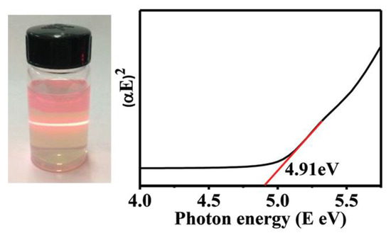
Figure 8.
Absorption energy, αE, vs. the photon energy, E, for the MoO3 nanosheet sample (black line). Red line shows the extrapolation for determining the band-gap energy. Adapted from ref. [44].
These features also extend to electrical ones. MoO3 nanosheet samples were found to exhibit significantly enhanced alcohol vapor sensing performance compared to the bulk MoO3. It also was found that both the sensor response and recovery time were reduced significantly [44].
Sun et al. described the synthesis of ultrathin two-dimensional transition metal oxide nanosheets [15]. According to time-dependent experiments, it was demonstrated that the size of the ultrathin SnO2 nanosheets can be controlled by adjusting the reaction time. The morphological and microstructural characteristics of thin 2D SnO2 nanosheets are clearly observed by electron microscopy techniques (Figure 9).
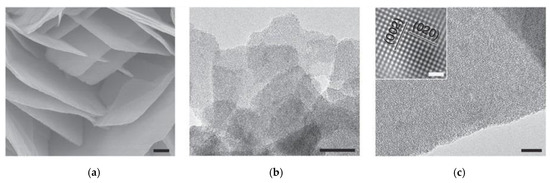
Figure 9.
Electron microscope images of 2D transition metal oxide nanosheets. SEM image (a); low-magnification TEM image (b); and high-magnification TEM image of WO3 sheets (c). Adapted with permission from ref. [15]. Scale bar, 200 nm (a), 20 nm (b), 5 nm (c), and 1 nm (insets in c).
SnO2 nanosheets were tested with gas molecules such as formaldehyde [45]. In accordance with the typical sensing mechanism of MOX sensors, the response is due to the reaction of formaldehyde with the adsorbed oxygen, HCHO + 2O−(ads) → CO2 + H2O + 2e−, which lead to electrons being fed back into the conductance band of SnO2, resulting in the decreasing potential barrier height. The thinning of the depletion layer by the direct conduction pathway decreases the sensor resistance of the ultrathin SnO2 nanosheets. When formaldehyde is out, the ultrathin SnO2 nanosheets sensor is exposed to air and rapidly recovers the high-resistance value again.
A recent review on ZnO nanosheets for gas sensing applications has been reported by Leonardi [46]. Liu et al. have prepared novel single-crystalline ZnO nanosheets with porous structures (see Figure 10) via annealing ZnS(en)0.5 (en = ethylenediamine) complex precursors [47]. Interestingly, there are numerous mesopores with a diameter of about 26.1 nm throughout each nanosheet with a high density. Besides, ZnO nanosheets gas sensors not only exhibit a good response and short response and recovery time, but also have long term stability for detecting formaldehyde with concentrations ranging from 5–100 ppm at the low operating temperature of 240 °C.
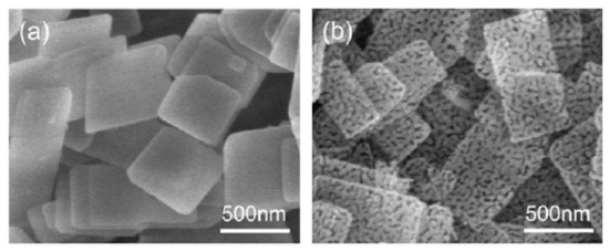
Figure 10.
(a) FESEM (Field Emission Scanning Electron Microscopy) images of the as-synthesized precursor; (b) porous ZnO nanosheets. Reprinted with permission from ref. [47].
Since gas-sensing properties of metal oxides are largely dependent on the surface atom structure of exposed facets, one of the most effective strategies to achieve enhanced performance is to maximize the percentage of exposed facets with higher reactivity. For example, TiO2 nanostructures with high-energy {001} facets should be in favour of exploring the gas-sensing properties and related mechanisms. Ultrathin anatase TiO2 nanosheets dominated by {001} facets were synthesized by Yang [48]. High performance gas sensors have been developed by means of these nanostructures [19].
4.3. TMDs Layered Materials
To date, several inorganic 2D TMDs layered materials including for example MoS2, WS2, MoSe, WSe2, and III-VI group semiconducting layered materials GaS and GaSe, have been reported and identified for possible gas sensing applications. So far, disulfides play the key role for gas sensing among the variety of TDMs materials.
In this specific class, MoS2 is the most dominating thin 2D non-graphene material in gas sensor applications owing to its ability to differentiate between a charge donor and an acceptor analyte. The MoS2 crystal (Figure 11) consists of a metal Mo layer sandwiched between two S layers, with these triple layers stacking together to form a layered structure [49]. The image of the as-synthesised MoS2 film on the 2-inch sapphire substrate reveals the semi-transparent characteristics of the as-synthesized film consisting of the three MoS2 layers. Raman characterization of the triple-layered MoS2 shows a strong in-plane vibrational mode for the Mo and S atoms (E2g) and an out-of-plane vibrational mode for the S atoms (A1g), with a peak difference (Δ) approximately equal to 22.9, indicating triple-layered MoS2 homogeneously distributed on the 50 × 50 μm2 area of the substrate surface.
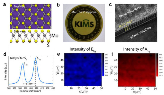
Figure 11.
(a) Schematic of the atomic-layered MoS2. The quasi-2D MoS2 was occupied by one Mo (a trigonal prismatic structure) and two S atoms (hexagonal planes); (b) Image of the as-synthesised MoS2 film on the 2-inch sapphire substrate. The as-synthesised MoS2 film was semi-transparent; (c) Cross-sectional TEM images of the as-grown MoS2 films. The image clearly demonstrates that the synthesised MoS2 films consisted of three layers of MoS2; (d) Raman spectrum of the triple-layered MoS2. The spectrum reveals a strong in-plane vibrational mode for the Mo and S atoms (E2g) and an out-of-plane vibrational mode for the S atoms (A1g). The peak position difference (Δ) between the E2g and A1g bands is approximately 22.9, indicating triple-layered MoS2; (e,f) Raman maps of E2g (blue) and A1g (red), respectively. The Raman mapping area was 50 × 50 μm2 with 0.3 μm steps. The Raman images show the spatial distribution on the surface of the substrates. Reprinted with permission from ref. [49].
MoS2 has demonstrated excellent sensing characteristics such as high sensitivity, fast response time, and good stability to a series of target gases [50,51,52,53,54,55,56]. For example, Kim et al. investigated the oxygen sensing behavior of MoS2 microflakes prepared by mechanical and liquid exfoliation, respectively [22]. The sensors show huge differences in sensing properties according to their fabrication methods. These differences may be attributed to the modified surface-to volume ratio and the consequent change in the number of edge sites. Liquid-exfoliated MoS2 nanoparticles with an increased number of edge sites present high and linear responses to a broad range of oxygen concentrations (1–100%). The authors pointed that, as far as they are aware, chemoresistive oxygen gas sensors with these outstanding sensing characteristics had never been achieved before.
SnS2 is another important sulfide semiconductor material with a wide band gap (Eg = 2.35 eV), known for its potential applications in efficient solar cells as well as electrical switching [57]. Chang et al. predicted that SnS2 nanostructures could be excellent sensor materials for NH3 detection [58]. Shi et al. fabricated gas sensors consisting of flower-like SnS2 nanostructures. The results showed that when the concentration of NH3 is as low as 5 ppm, the sensitivity could reach as high as 21.6% at room temperature [59]. SnS2 nanoflakes have been also reported for efficient humidity and alcohol sensing at room temperature [60]. At the same time, the SnS2 nanoflakes based alcohol sensing properties towards methanol, ethanol, and iso-propyl alcohol have been also investigated. The humidity sensing behavior of the SnS2 nanoflake sensor device was studied in the range of 11–97% relative humidity (RH) at room temperature. The response time of ~85 s and recovery time of ~6 s were observed for the SnS2 nanoflake based humidity sensor. A maximum response (S = R/R0) of 11,300% was recorded at 97% RH. An exclusive selectivity towards methanol is shown as compared to other analytes. The response time of ~67 s and recovery time of just 5 s were observed for the SnS2 nanoflake based methanol sensor. SnS2 nanoflakes were also proposed as promising sensors for oxygen at low temperature [61].
WS2 and VS2 have also been investigated for gas sensing. High quality monolayer WS2 may pave the way for developing industrial-scale optoelectronic devices for photo-detecting and chemical sensing applications [62,63]. Figure 12 shows one of these devices and the results obtained under gas molecules both in dark and under light illumination. The drain current of the FET (Field Effect Transistor) device decreased in O2 and air, but increased in ethanol and NH3, compared to that under vacuum. The current change is considered to result from the charge transfer between the WS2 nanoflakes and the adsorbed gas molecules.
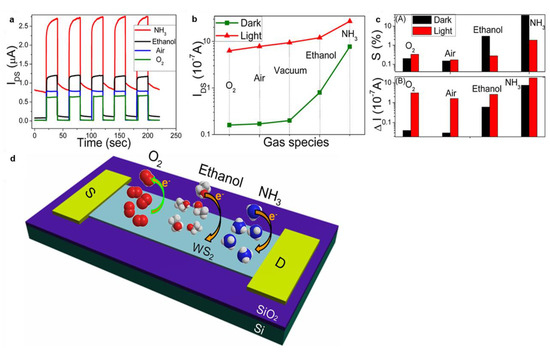
Figure 12.
Electrical and sensing characteristics of a WS2 nanoflakes transistor. (a) Time-dependent photocurrent response under various gas atmospheres; (b) The extracted dark current and photocurrent under different gas atmospheres; (c) Gas sensitivity (A) and current change (B) under different conditions; (d) Schematic diagram of the charge transfer process between the adsorbed gas molecules and the WS2 nanoflakes transistor. Adapted from ref. [63].
Once the vapor molecules come into contact with the surface of WS2, the gas molecule is expected to be adsorbed and subsequently change the charge carrier distribution in the WS2 nanoflakes. O2 molecules can act as electron acceptors from WS2, leading to a reduction in the overall conductivity. In contrast, ethanol and NH3 molecules, serving as electron donors, enhance the total conducting electron density of WS2 nanoflakes, resulting in an increased current. WS2 nanoflakes are also selective for NH3; as suggested by Li et al., the presence of sulfide species, acting as Lewis acids, on the WS2 nanoflakes’ surface, are responsible for this behavior, due to the selective interaction of these acid sites with ammonia molecules [64].
WS2 nanosheets were used as a sensing material to fabricate a humidity sensor on interdigitated aluminum electrodes, realized on Si/SiO2 substrates using a conventional photolithography technique [65]. The response of the sensor (S = R/R0) varied from 11.9 for 40% RH to as high as 37.5 for 80% RH. The response and recovery times were found to be 13 ± 2 s and 17 ± 2 s, respectively. Kuru et al. reported a flexible hydrogen sensor, composed of a WS2 nanosheet–Pd nanoparticle composite film, fabricated on a flexible polyimide substrate [66]. The sensor offers the advantages of being light-weight, mechanical durability, room temperature operation, and high sensitivity. Moreover, the WS2–Pd composite film distinctly outperforms the graphene–Pd composite. VS2 ultrathin nanosheets were also investigated as humidity sensors for novel touchless positioning interfaces [67].
Selenide and telluride are other classes of TMDs materials with thin 2D nanostructures which have been also investigated for their sensing properties [68,69]. A study of adsorption sites on monolayer PtSe2, consisting of Pt atoms sandwiched between Se atoms such that a top view shows a hexagonal structure with Pt and Se atoms located at alternating corners and an additional Se atom in the center of each hexagon, indicate its promising characteristics for superior gas sensing [70]. Duesberg and coworkers demonstrated the potential of PtSe2 in a range of applications [71]. As a gas sensor, PtSe2 had extremely high sensitivity, measuring 100 ppb NO2 at room temperature, was extremely fast to respond to the gas—detecting low quantities of gas in only seconds—and recovered completely within a minute when the inert atmosphere was restored.
5. Thin 2D Nanostructure and Heterostructure-Based Composites for Gas Sensing
The possibility to create hierarchical structures by assembling thin 2D inorganic nanostructures, along with the combination of two or more thin 2D materials, has been largely exploited as a strategy for expanding/tuning the electrical, optical, electrochemical characteristics of the single components. These composite nanostructures and heterostructures have also been used as sensing materials in conductometric devices for enhancing the gas sensing capabilities of the single components. Below, an outline of the sensing performances of these 2D nanostructures is briefly presented.
5.1. Assembled Thin 2D Materials
An attractive aspect of thin 2D inorganic materials is that they can be organized into various hierarchical nanostructures, exhibiting excellent gas sensing properties. Thin 2D nanosheets facilitate the formation of architectural building blocks to be assembled into a variety of nanostructures (see Figure 13) which endows hollow-structured materials with tunable properties [72].
Figure 13.
Example of the formation of architectural building blocks to be assembled into a variety of nanostructures which endows hollow-structured materials. Reprinted with permission from ref. [72].
Huang and coworkers prepared hierarchical nanorods assembled by interlaced ultrathin nanosheets (with a thickness of around 3 nm), that possessed a large specific surface area and a novel open-style pore structure, which endowed it with large amount of gas adsorption and rapid gas diffusion [73,74]. Hollow and hollowed-out Co3O4 microspheres were assembled by porous ultrathin nanosheets with a thickness of about 3 nm that were synthesized via a new rapid and energy-efficient room temperature interfacial-reaction. As expected, the gas sensor based on these assembled materials exhibited a high response and ultra-fast response/recovery speed (both the response and recovery time were 1 s) when detecting a low concentration of ethanol [73].
By using the same preparation procedure [74], they also prepared hollowed-out hierarchical α-Fe2O3 nanorods. A transient response to different concentrations of acetone is reported in Figure 14. The inset shows the response to 100 ppm of different gases. Hollowed-out hierarchical α-Fe2O3 nanorods exhibit a high response and fast response and recovery speed (the response/recovery time of the gas sensor to 100 ppm acetone and ethanol are 0.4/2.4 s and 0.8/3.2 s, respectively). Notably, this high response and the ultra-fast response/recovery speed of the sensor are related to the hollow and hollowed-out nanostructures assembled by the porous ultrathin nanosheets.
Figure 14.
Transient response of α-Fe2O3 nanorods to different concentrations of acetone. The inset shows the response to 100 ppm of different gases. Reprinted with permission from ref. [74].
Unusual 3D flower-shaped SnS2 nanostructures have been synthesized using a mild hydrothermal treatment in the presence of octyl-phenol-ethoxylate (Triton X-100) at 160 °C [59]. The nanostructures have an average size of 1 μm, and consist of interconnected nanosheets with thicknesses of about 40 nm. Based on time-dependent experimental results, the authors ascribe the oriented attachment mechanism to the growth of the SnS2 nanostructures. The nonionic surfactant Triton X-100 plays a key role in the formation of the flower-like morphology. Room temperature gas-sensing measurements show that the 3D SnS2 nanostructures could serve as sensor materials for the detection of NH3 molecules. The observed behavior can be attributed to the presence of atomically thin layers with perfect crystallinity within planar directions. A high performance towards NH3 is then favored by the increased surface area as well as the concentration of the charge carrier and carrier charge mobility of these nanostructures.
Hierarchical flower-like Ni–Al-layered double hydroxide intercalation (NFA-LDHs) compounds were synthesized by Hong and coworkers through a facile one-step hydrothermal method using sodium dodecyl sulfate (SDS) as the intercalation layer and template [75]. The enhanced gas sensing of these thin 2D LDHs can be ascribed to the unique hierarchical porous structure and the highly oriented layered single crystal structure and composition, which can enhance the conductivity/carrier densities, fast carrier transportation, and gas adsorption–desorption, and provide a large number of active sites for surface contact reactions. Thus, the NFA 1-1 sensor exhibits a greater response and a fast response time.
5.2. TMDs Heterostructures
As compared to the corresponding pure monolayer systems, heterostructures based on TMDs are subject to significant modifications of their electronic properties [76]. Due to the layered structures of these 2D nanomaterials, the formation of heterostructures can be in the vertical or lateral fashion. However, despite their technological relevance, the properties that can be expected from such systems are still largely unknown. At the same time, challenges still exist regarding the reliable synthesis of TDMs heterostructures. Kang and coworkers reported a one-step growth for high-quality vertically stacked and in-plane interconnected heterostructures of WS2/MoS2 via control of the growth temperature [77]. Vertically stacked bilayers with WS2 epitaxially grown on top of the MoS2 monolayer are formed with the preferred stacking order at high temperature (Figure 15). A strong interlayer excitonic transition is observed due to the type II band alignment and to the clean interface of these bilayers. Vapour growth at low temperature, on the other hand, leads to lateral epitaxy of WS2 on the MoS2 edges, creating seamless in-plane heterostructures that generate strong localized photoluminescence enhancement and intrinsic p–n junctions.
Figure 15.
(a) Vertical and (e) in-plane heterostructures from WS2/MoS2 monolayers. Optical and SEM images of (b–d) vertical and (f–g) in-plane WS2/MoS2 heterostructures. Reprinted with permission from ref. [77].
Theoretical studies have revealed that WS2/MoS2 monolayer heterojunctions can align their band structures to be suitable for potential gas applications. It is expected that the electrical resistivity of the lateral TMDs heterojunctions would be affected by the adsorbed molecules, especially on their in-plane interface [78]. Calculations show that the molecule adsorption significantly affects the electronic transport properties of the heterojunction. Such sensitivity to adsorption makes the heterojunction a superior gas sensor that promises wide-ranging applications.
5.3. Thin 2D Graphene/Inorganic Composites
The possibility of using a combination of graphene with different thin 2D inorganic materials may lead to new 2-dimensional hybrid nanostructures with exciting properties. The high surface area, and highly conducting and electroactive nature of graphene have been exploited to design novel layered graphene-transition metal dichalcogenide hybrids [79]. Functionalizing graphene surfaces with thin 2D inorganic materials provides a promising platform for the development of effective gas sensors because of the band-gap, which leads to a selective synergistic effect [80]. Furthermore, these composites overcome the main problem of the agglomeration of the graphene sheets, offering new opportunities to enhance the interaction of the target gas with all the layers, and leads to a full utilization of the high surface area offered by the layered structures [81]. Figure 16 describes an example of such a hybrid nanostructure.
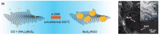
Figure 16.
Solvothermal synthesis with GO sheets to afford the MoS2/rGO hybrid; (a) synthesis pathway; (b) SEM and TEM images (inset) of the hybrid. Adapted with permission from ref. [82].
Recently, the gas sensing performance of a MoS2/rGO hybrid thin 2D heterostructure prepared via the combination of mechanically exfoliated MoS2 and CVD grown graphene has been described by Cho et al. [83]. The gas response characteristics of the MoS2/rGO heterostructure on a flexible substrate were retained without serious performance degradation, even under mechanical deformation, promising to provide a simple sensing platform for wearable electronics.
6. Conclusions
The impressive research made in recent years on thin 2D layered inorganic materials contributes to the understanding of many of their fascinating properties. This is the basis for solving some challenges that still remain regarding the use of these materials for many applications. As pointed out in this feature paper, recent advances in thin 2D inorganic nanomaterials point to promising prospects for the development of novel gas sensing applications, due to their distinctive and unique physical, chemical, and electronic properties. However, studies to date indicate that there are still significant improvements to be made before these materials can be used for practical applications. In this regard, the preparation of well defined, reproducible, and large-scale quantities of these two-dimensional materials needs to be addressed. Certainly, other various technological issues need to be overcome; nevertheless, it looks promising for gas sensing applications, which are difficult to realize with conventional materials.
Acknowledgments
This work was carried out with financial assistance from the University of Messina under the framework of the “Research & Mobility 2016” project.
Conflicts of Interest
The author declares no conflict of interest.
References
- Huang, X.; Tan, C.; Yin, Z.; Zhang, H. 25th anniversary article: Hybrid nanostructures based on two-dimensional nanomaterials. Adv. Mater. 2014, 26, 2185–2204. [Google Scholar] [CrossRef] [PubMed]
- Wang, Q.H.; Kalantar-Zadeh, K.; Kis, A.; Coleman, J.N.; Strano, M.S. Electronics and optoelectronics of two-dimensional transition metal dichalcogenides. Nat. Nanotechnol. 2012, 7, 699–712. [Google Scholar] [CrossRef] [PubMed]
- Sun, Y.; Lei, F.; Gao, S.; Pan, B.; Zhou, J.; Xie, Y. Atomically thin tin dioxide sheets for efficient catalytic oxidation of carbon monoxide. Angew. Chem. 2013, 125, 10763–10766. [Google Scholar] [CrossRef]
- Late, D.J.; Liu, B.; Matte, H.S.S.R.; Dravid, V.P.; Rao, C.N.R. Hysteresis in single-layer MoS2 field effect transistors. ACS Nano 2012, 6, 5635. [Google Scholar] [CrossRef] [PubMed]
- Novoselov, K.S.; Geim, A.K.; Morozov, S.V.; Jiang, D.; Zhang, Y.; Dubonos, S.V.; Grigorieva, I.V.; Firsov, A.A. Electric field effect in atomically thin carbon films. Science 2004, 306, 666–669. [Google Scholar] [CrossRef] [PubMed]
- Gupta, A.; Sakthivel, T.; Seal, S. Recent development in 2D materials beyond graphene. Prog. Mater. Sci. 2015, 73, 44–126. [Google Scholar] [CrossRef]
- Mas-Ballesté, R.; Gómez-Navarro, C.; Gómez-Herrero, J.; Zamora, F. 2D materials: To graphene and beyond. Nanoscale 2011, 3, 20–30. [Google Scholar] [CrossRef] [PubMed]
- Zhang, H. Ultrathin two-dimensional nanomaterials. ACS Nano 2015, 9, 9451–9469. [Google Scholar] [CrossRef] [PubMed]
- Wang, Q.; O’Hare, D. Recent advances in the synthesis and application of layered double hydroxide (LDH) nanosheets. Chem. Rev. 2012, 112, 4124–4155. [Google Scholar] [CrossRef] [PubMed]
- Polese, D.; Mattoccia, A.; Giorgi, F.; Pazzini, L.; Ferrone, A.; Di Giamberardino, L.; Maiolo, L.; Pecora, A.; Convertino, A.; Fortunato, G.; et al. Layered double hydroxides intercalated with chlorine used as low temperature gas sensors. Proc. Eng. 2015, 120, 1175–1178. [Google Scholar] [CrossRef]
- Morandi, S.; Prinetto, F.; Di Martino, M.; Ghiotti, G.; Lorret, O.; Tichit, D.; Malagù, C.; Vendemiati, B.; Carotta, M.C. Synthesis and characterisation of gas sensor materials obtained from Pt/Zn/Al layered double hydroxides. Sens. Actuators B Chem. 2006, 118, 215–220. [Google Scholar] [CrossRef]
- Yin, H.; Tang, Z. Ultrathin two-dimensional layered metal hydroxides: An emerging platform for advanced catalysis, energy conversion and storage. Chem. Soc. Rev. 2016, 45, 4873–4891. [Google Scholar] [CrossRef] [PubMed]
- Xu, Q.H.; Xu, D.M.; Guan, M.Y.; Guo, Y.; Qi, Q.; Li, G.D. ZnO/Al2O3/CeO2 composite with enhanced gas sensing performance. Sens. Actuators B Chem. 2013, 177, 1134–1141. [Google Scholar] [CrossRef]
- Neri, G. First fifty years of chemoresistive gas sensors. Chemosensors 2015, 3, 1–20. [Google Scholar] [CrossRef]
- Sun, Z.; Liao, T.; Dou, Y.; Hwang, S.M.; Park, M.-S.; Jiang, L.; Kim, J.H.; Dou, S.X. Generalized self-assembly of scalable two-dimensional transition metal oxide nanosheets. Nat. Commun. 2014, 5, 3813. [Google Scholar] [CrossRef] [PubMed]
- Radisavljevic, B.; Radenovic, A.; Brivio, V.; Giacometti, J.; Kis, A. Single-layer MoS2 transistors. Nat. Nanotechnol. 2011, 6, 147. [Google Scholar] [CrossRef] [PubMed]
- Coleman, J.N.; Lotya, M.; O’Neill, A.; Bergin, S.D.; King, P.J.; Khan, U.; Young, K.; Gaucher, A.; De, S.; Smith, R.J.; et al. Two-dimensional nanosheets produced by liquid exfoliation of layered materials. Science 2011, 331, 568. [Google Scholar] [CrossRef] [PubMed]
- Kim, T.H.; Kim, Y.H.; Park, S.Y.; Kim, S.Y.; Jang, H.W. Two-Dimensional Transition Metal Disulfides for Chemoresistive Gas Sensing: Perspective and Challenges. Chemosensors 2017, 5, 15. [Google Scholar] [CrossRef]
- Liu, C.; Lu, H.; Zhang, J.; Yang, Z.; Zhu, G.; Yin, F.; Gao, J.; Chen, C.; Xin, X. Abnormal p-type sensing response of TiO2 nanosheets with exposed {001} facets. J. Alloy. Compd. 2017, 705, 112–117. [Google Scholar] [CrossRef]
- Shavanova, K.; Bakakina, Y.; Burkova, I.; Shtepliuk, I.; Viter, R.; Ubelis, A.; Beni, V.; Starodub, N.; Yakimova, R.; Khranovskyy, V. Application of 2D non-graphene materials and 2D oxide nanostructures for biosensing technology. Sensors 2016, 16, 223. [Google Scholar] [CrossRef] [PubMed]
- Mak, K.F.; Lee, C.; Hone, J.; Shan, J.; Heinz, T.F. Atomically thin MoS2: A new direct-gap semiconductor. Phys. Rev. Lett. 2010, 105, 136805. [Google Scholar] [CrossRef] [PubMed]
- Kim, Y.H.; Kim, K.Y.; Choi, Y.R.; Shim, Y.-S.; Jeon, J.-M.; Lee, J.-H.; Kim, S.Y.; Han, S.; Jang, H.W. Ultrasensitive reversible oxygen sensing by using liquid-exfoliated MoS2 nanoparticles. J. Mater. Chem. A 2016, 4, 6070–6076. [Google Scholar] [CrossRef]
- Nah, J.; Kumar, S.B.; Fang, H.; Chen, Y.-Z.; Plis, E.; Chueh, Y.-L.; Krishna, S.; Guo, J.; Javey, A. Quantum size effects on the chemical sensing performance of two-dimensional semiconductors. J. Phys. Chem. C 2012, 116, 9750–9754. [Google Scholar] [CrossRef]
- Gurlo, A.; Riedel, R. In situ and operando spectroscopy for assessing mechanisms of gas sensing. Angew. Chem. 2007, 46, 3826–3848. [Google Scholar] [CrossRef] [PubMed]
- Liu, B.L.; Chen, L.; Liu, G.; Abbas, A.N.; Fathi, M.; Zhou, C.W. High-performance chemical sensing using Schottky-contacted chemical vapor deposition grown monolayer MoS2 transistors. ACS Nano 2014, 8, 5304–5314. [Google Scholar] [CrossRef] [PubMed]
- Zhang, J.; Liu, X.; Neri, G.; Pinna, N. Nanostructured materials for room-temperature gas sensors. Adv. Mater. 2016, 28, 795–831. [Google Scholar] [CrossRef] [PubMed]
- Ou, J.Z.; Ge, W.; Carey, B.; Daeneke, T.; Rotbart, A.; Shan, W.; Wang, Y.; Fu, Z.; Chrimes, A.F.; Wlodarski, W.; et al. Physisorption-based charge transfer in two-dimensional SnS2 for selective and reversible NO2 gas sensing. ACS Nano 2015, 9, 10313–10323. [Google Scholar] [CrossRef] [PubMed]
- Kannan, P.K.; Late, D.J.; Morgan, H.; Rout, C.S. Recent developments in 2D layered inorganic nanomaterials for sensing. Nanoscale 2015, 7, 13293–13312. [Google Scholar] [CrossRef] [PubMed]
- Wang, J.; Li, G.; Li, L. Synthesis Strategies about 2D Materials in Two-Dimensional Materials—Synthesis, Characterization and Potential Applications; Nayak, P.K., Ed.; Intech: Rijeka, Croatia, 2016. [Google Scholar]
- Sun, Y.F.; Cheng, H.; Gao, S.; Liu, Q.H.; Sun, Z.H.; Xiao, C.; Wu, C.Z.; Wei, S.Q.; Xie, Y. Atomically thick bismuth selenide freestanding single layers achieving enhanced thermoelectric energy harvesting. J. Am. Chem. Soc. 2012, 134, 20294. [Google Scholar] [CrossRef] [PubMed]
- Li, H.; Wu, J.; Yin, Z.Y.; Zhang, H. Preparation and applications of mechanically exfoliated single and multi-layer MoS2 and WSe2 nanosheets. Acc. Chem. Res. 2014, 47, 1067–1075. [Google Scholar] [CrossRef] [PubMed]
- Li, H.; Lu, G.; Wang, Y.; Yin, Z.; Cong, C.; He, Q.; Wang, L.; Ding, F.; Yu, T.; Zhang, H. Mechanical exfoliation and characterization of single and few-layer nanosheets of WSe2, TaS2, and TaSe2. Small 2013, 9, 1974–1981. [Google Scholar] [CrossRef] [PubMed]
- Kang, J.-G.; Ko, Y.-D.; Choi, K.J.; Park, J.-G.; Kim, D.-W. Fabrication of tin monosulfide nanosheet arrays using laser ablation. Appl. Phys. A 2011, 103, 505–510. [Google Scholar] [CrossRef]
- Yoo, D.; Kim, M.; Jeong, S.; Han, J.; Cheon, J. Chemical synthetic strategy for single-layer transition-metal chalcogenides. J. Am. Chem. Soc. 2014, 136, 14670–14673. [Google Scholar] [CrossRef] [PubMed]
- Du, Y.P.; Yin, Z.Y.; Zhu, J.X.; Huang, X.; Wu, X.J.; Zeng, Z.Y.; Yan, Q.Y.; Zhang, H. A general method for the large-scale synthesis of uniform ultrathin metal sulphide nanocrystals. Nat. Commun. 2012, 3, 1177. [Google Scholar] [CrossRef] [PubMed]
- Zhang, H. Single-layer semiconducting nanosheets: High-yield preparation and device fabrication. Angew. Chem. 2011, 50, 11093–11097. [Google Scholar] [CrossRef] [PubMed]
- Lin, Z.; McCreary, A.; Briggs, N.; Subramanian, S.; Zhang, K.; Sun, Y.; Li, X.; Borys, N.J.; Yuan, H.; Fullerton-Shirey, S.K.; et al. 2D materials advances: From large scale synthesis and controlled heterostructures to improved characterization techniques, defects and applications. 2D Mater. 2016, 3, 042001. [Google Scholar] [CrossRef]
- Lee, K.; Gatensby, R.; McEvoy, N.; Hallam, T.; Duesberg, G.S. High-performance sensors based on molybdenum disulfide thin films. Adv. Mater. 2013, 25, 6699–6702. [Google Scholar] [CrossRef] [PubMed]
- Di Francia, G.; Alfano, B.; La Ferrara, V. Conductometric gas nanosensors. J. Sens. 2009, 2009, 659275:1–659275:19. [Google Scholar] [CrossRef]
- Zhang, L.; Li, F.; Evans, D.; Duan, X. Structure and surface characteristics of Cu-based composite metal oxides derived from layered double hydroxides. Mater. Chem. Phys. 2004, 87, 402–410. [Google Scholar] [CrossRef]
- Osada, M.; Sasaki, T. Exfoliated oxide nanosheets: New solution to nanoelectronics. J. Mater. Chem. 2009, 19, 2503–2511. [Google Scholar] [CrossRef]
- Osada, M.; Sasaki, T. Two-Dimensional Dielectric Nanosheets: Novel Nanoelectronics From Nanocrystal Building Blocks. Adv. Mater. 2012, 24, 210. [Google Scholar] [CrossRef] [PubMed]
- Patil, S.J.; Patil, A.V.; Dighavkar, C.G.; Thakare, K.S.; Borase, R.Y.; Nandre, S.J.; Deshpande, N.G.; Ahire, R.R. Semiconductor metal oxide compounds based gas sensors: A literature review. Front. Mater. Sci. 2015, 9, 14–37. [Google Scholar] [CrossRef]
- Ji, F.; Ren, X.; Zheng, X.; Liu, Y.; Pang, L.; Jiang, J.; Liu, S. 2D-MoO3 nanosheets for superior gas sensors. Nanoscale 2016, 8, 8696. [Google Scholar] [CrossRef] [PubMed]
- Yu, H.; Yang, T.; Zhao, R.; Xiao, B.; Li, Z.; Zhang, M. Fast formaldehyde gas sensing response properties of ultrathin SnO2 nanosheets. RSC Adv. 2015, 5, 104574–104581. [Google Scholar] [CrossRef]
- Leonardi, S.G. Two-Dimensional Zinc Oxide Nanostructures for Gas Sensor Applications. Chemosensors 2017, 5, 17. [Google Scholar] [CrossRef]
- Liu, J.Y.; Guo, Z.; Meng, F.L.; Luo, T.; Li, M.Q.; Liu, J.H. Novel porous single-crystalline ZnO nanosheets fabricated by annealing ZnS(en)(0.5) (en = ethylenediamine) precursor. Application in a gas sensor for indoor air contaminant detection. Nanotechnology 2009, 20, 125501. [Google Scholar] [CrossRef] [PubMed]
- Yang, X.H.; Li, Z.; Liu, G.; Xing, J.; Sun, C.H.; Yang, H.G.; Li, C.Z. Ultra-thin anatase TiO2 nanosheets dominated with {001} facets: Thickness-controlled synthesis, growth mechanism, and water-splitting properties. CrystEngComm 2011, 13, 1378–1383. [Google Scholar] [CrossRef]
- Cho, B.; Hahm, M.G.; Choi, M.; Yoon, J.; Kim, A.R.; Lee, Y.-J.; Park, S.-G.; Kwon, J.-D.; Kim, C.S.; Song, M.; et al. Charge-transfer-based gas sensing using atomic-layer MoS2. Sci. Rep. 2015, 5, 8052. [Google Scholar] [CrossRef] [PubMed]
- Li, H.; Yin, Z.; He, Q.; Li, H.; Huang, X.; Lu, G.; Fam, D.W.H.; Tok, A.I.Y.; Zhang, Q.; Zhang, H. Fabrication of single- and multilayer MoS2 film-based field-effect transistors for sensing NO at room temperature. Small 2012, 8, 63–67. [Google Scholar] [CrossRef] [PubMed]
- He, Q.; Zeng, Z.; Yin, Z.; Li, H.; Wu, S.; Huang, X.; Zhang, H. Fabrication of flexible MoS2 thin-film transistor arrays for practical gas-sensing applications. Small 2012, 8, 2994–2999. [Google Scholar] [CrossRef] [PubMed]
- Late, D.J.; Huang, Y.-K.; Liu, B.; Acharya, J.; Shirodkar, S.N.; Luo, J.; Yan, A.; Charles, D.; Waghmare, U.V.; Dravid, V.; et al. Sensing behavior of atomically thin-layered MoS2 transistors. ACS Nano 2013, 7, 4879–4891. [Google Scholar] [CrossRef] [PubMed]
- Perkins, F.K.; Friedman, A.L.; Cobas, E.; Campbell, P.M.; Jernigan, G.G.; Jonker, B.T. Chemical vapor sensing with monolayer MoS2. Nano Lett. 2013, 13, 668–673. [Google Scholar] [CrossRef] [PubMed]
- Donarelli, M.; Prezioso, S.; Perrozzi, F.; Bisti, F.; Nardone, M.; Giancaterini, L.; Cantalini, C.; Ottaviano, L. Response to NO2 and other gases of resistive chemically exfoliated MoS2-based gas sensors. Sens. Actuators B Chem. 2015, 207, 602–613. [Google Scholar] [CrossRef]
- Cho, B.; Kim, A.R.; Park, Y.; Yoon, J.; Lee, Y.-J.; Lee, S.; Yoo, T.J.; Kang, C.G.; Lee, B.H.; Ko, H.C.; Kim, D.-H.; Hahm M., G. Bifunctional sensing characteristics of chemical vapor deposition synthesized atomic-layered MoS2. ACS Appl. Mater. Interfaces 2015, 7, 2952–2959. [Google Scholar] [CrossRef] [PubMed]
- Yao, Y.; Tolentino, L.; Yang, Z.; Song, X.; Zhang, W.; Chen, Y.; Wong, C. High-concentration aqueous dispersions of MoS2. Adv. Funct. Mater. 2013, 23, 3577. [Google Scholar] [CrossRef]
- Brousse, T.; Lee, S.M.; Pasquereau, L.; Defives, D.; Schleich, D.M. Composite negative electrodes for lithium ion cells. Solid State Ionics 1998, 115, 51–56. [Google Scholar] [CrossRef]
- Chang, H.J.; In, E.; Kong, K.J.; Lee, J.O.; Choi, Y.M.; Ryu, B.H. First-principles studies of SnS2 nanotubes: A potential semiconductor nanowire. J. Phys. Chem. B 2005, 109, 30–32. [Google Scholar] [CrossRef] [PubMed]
- Shi, W.; Huo, L.; Wang, H.; Zhang, H.; Yang, J.; Wei, P. Hydrothermal growth and gas sensing property of flower-shaped SnS2 nanostructures. Nanotechnology 2006, 17, 2918–2924. [Google Scholar] [CrossRef]
- Bharatula, L.D.; Erande, M.B.; Mulla, I.S.; Rout, C.S.; Late, D.J. SnS2 nanoflakes for efficient humidity and alcohol sensing at room temperature. RSC Adv. 2016, 6, 105421–105427. [Google Scholar] [CrossRef]
- Li, Y.; Leonardi, S.G.; Bonavita, A.; Neri, G.; Wlodarski, W. Two-dimensional (2D) SnS2-based oxygen sensor. Procedia Eng. 2016, 168, 1102–1105. [Google Scholar] [CrossRef]
- Lan, C.; Li, C.; Yin, Y.; Liu, Y. Large-area synthesis of monolayer WS2 and its ambient-sensitive photo-detecting performance. Nanoscale 2015, 7, 5974–5980. [Google Scholar] [CrossRef] [PubMed]
- Huo, N.; Yang, S.; Wei, Z.; Li, S.-S.; Xia, J.-B.; Li, J. Photoresponsive and gas sensing field-effect transistors based on multilayer WS2 nanoflakes. Sci. Rep. 2014, 4, 5209. [Google Scholar] [CrossRef] [PubMed]
- Li, X.; Li, X.; Li, Z.; Wang, J.; Zhang, J. WS2 nanoflakes based selective ammonia sensors at room temperature. Sens. Actuators B Chem. 2017, 240, 273–277. [Google Scholar] [CrossRef]
- Jha, R.K.; Guha, P.K. Liquid exfoliated pristine WS2 nanosheets for ultrasensitive and highly stable chemiresistive humidity sensors. Nanotechnology 2016, 27, 475503. [Google Scholar] [CrossRef] [PubMed]
- Kuru, C.; Choi, D.; Kargar, A.; Liu, C.H.; Yavuz, S.; Choi, C.; Jin, S.; Bandaru, P.R. High-performance flexible hydrogen sensor made of WS2 nanosheet–Pd nanoparticle composite film. Nanotechnology 2016, 27, 195501. [Google Scholar] [CrossRef] [PubMed]
- Feng, J.; Peng, L.; Wu, C.; Sun, X.; Hu, S.; Lin, C.; Dai, J.; Yang, J.; Xie, Y. Ultrathin nanosheets: Giant moisture responsiveness of VS2 ultrathin nanosheets for novel touchless positioning interface. Adv. Mater. 2012, 24, 1969–1974. [Google Scholar] [CrossRef] [PubMed]
- Late, D.J.; Doneux, T.; Bougouma, M. Single-layer MoSe2 based NH3 gas sensor. Appl. Phys. Lett. 2014, 105, 233103. [Google Scholar] [CrossRef]
- Feng, Z.; Xie, Y.; Chen, J.; Yu, Y.; Zheng, S.; Zhang, R.; Li, Q.; Chen, X.; Sun, C.; Zhang, H. Highly sensitive MoTe2 chemical sensor with fast recovery rate through gate biasing. 2D Mater. 2017, 4, 025018. [Google Scholar] [CrossRef]
- Sajjad, M.; Montes, E.; Singh, N.; Schwingenschlög, U. Superior gas sensing properties of monolayer PtSe2. Adv. Mater. Interfaces 2017, 4, 1600911. [Google Scholar] [CrossRef]
- Yim, C.; Lee, K.; McEvoy, N.; O’Brien, M.; Riazimehr, S.; Berner, N.C.; Cullen, C.P.; Kotakoski, J.; Meyer, J.C.; Lemme, M.C.; et al. High-performance hybrid electronic devices from layered PtSe2 films grown at low temperature. ACS Nano 2016, 10, 9550–9558. [Google Scholar] [CrossRef] [PubMed]
- Zeng, Y.; Wang, Y.; Qiao, L.; Bing, Y.; Zou, B.; Zheng, W. Synthesis and the improved sensing properties of hierarchical SnO2 hollow nanosheets with mesoporous and multilayered interiors. Sens. Actuators B Chem. 2016, 222, 354–361. [Google Scholar] [CrossRef]
- Tan, J.; Dun, M.; Li, L.; Zhao, J.; Tan, W.; Lin, Z.; Huang, X. Synthesis of hollow and hollowed-out Co3O4 microspheres assembled by porous ultrathin nanosheets for ethanol gas sensors: Responding and recovering in one second. Sens. Actuators B Chem. 2017, 249, 44–52. [Google Scholar] [CrossRef]
- Tan, J.; Huang, X. Ultra-thin nanosheets-assembled hollowed-out hierarchical α-Fe2O3 nanorods: Synthesis via an interface reaction route and its superior gas sensing properties. Sens. Actuators B Chem. 2016, 237, 159–166. [Google Scholar] [CrossRef]
- Hong, D.; Zhang, J.; Rehman, A.U.; Gong, L.; Zhou, J.; Kan, K.; Li, L.; Shi, K. One-step synthesis of hierarchical Ni–Fe–Al layered double hydroxide with excellent sensing properties for NOx at room temperature. RSC Adv. 2016, 6, 103192–103198. [Google Scholar] [CrossRef]
- Kang, J.; Tongay, S.; Zhou, J.; Li, J.; Wu, J. Band offsets and heterostructures of two-dimensional semiconductors. Appl. Phys. Lett. 2013, 102, 012111. [Google Scholar] [CrossRef]
- Gong, Y.; Lin, J.; Wang, X.; Shi, G.; Lei, S.; Lin, Z.; Zou, X.; Ye, G.; Vajtai, R.; Yakobson, B.I.; et al. Vertical and in-plane heterostructures from WS2/MoS2 monolayers. Nat. Mater. 2014, 13, 1135–1142. [Google Scholar] [CrossRef] [PubMed]
- Sun, J.; Lin, N.; Ren, H.; Tang, C.; Yang, L.; Zhao, X. Gas adsorption on MoS2/WS2 in-plane heterojunctions and the I–V response: A first principles study. RSC Adv. 2016, 6, 17494. [Google Scholar] [CrossRef]
- Chua, C.K.; Loo, A.H.; Pumera, M. Nanostructured MoS2 nanorose/graphene nanoplatelet hybrids for electrocatalysis. Chem. Eur. J. 2016, 22, 5969. [Google Scholar] [CrossRef] [PubMed]
- Kumar, N.A.; Dar, M.A.; Gul, R.; Baek, J.-B. Graphene and molybdenum disulfide hybrids: Synthesis and applications. Mater. Today 2015, 18, 286–298. [Google Scholar] [CrossRef]
- Mohan, P.; Yang, J.; Jena, A.; Shin, H.S. VS2/rGO hybrid nanosheets prepared by annealing of VS4/rGO. J. Solid State Chem. 2015, 224, 82–87. [Google Scholar] [CrossRef]
- Li, Y.; Wang, H.; Xie, L.; Liang, Y.; Hong, G.; Dai, H. MoS2 nanoparticles grown on graphene: An advanced catalyst for the hydrogen evolution reaction. J. Am. Chem. Soc. 2011, 133, 7296. [Google Scholar] [CrossRef] [PubMed]
- Cho, B.; Yoon, J.; Lim, S.K.; Kim, A.R.; Kim, D.-H.; Park, S.-G.; Kwon, J.-D.; Lee, Y.-J.; Lee, K.-H.; Lee, B.H.; et al. Chemical sensing of 2D graphene/MoS2 heterostructure device. ACS Appl. Mater. Interfaces 2015, 7, 16775–16780. [Google Scholar] [CrossRef] [PubMed]


© 2017 by the author. Licensee MDPI, Basel, Switzerland. This article is an open access article distributed under the terms and conditions of the Creative Commons Attribution (CC BY) license (http://creativecommons.org/licenses/by/4.0/).