Abstract
Gas sensors based on carbon nanotubes (CNTs) as channel materials have been widely considered as promising candidates for the detection of toxic gas. However, effectively detecting methane (CH4) with CNTs-based sensors remains challenging because nonpolar CH4 molecules find it difficult to directly interact with CNTs. Herein, a functionalized CNTs-based thin-film transistor (TFT) sensor is proposed for the highly effective detection of CH4 at room temperature, where CNTs with high semiconductor purity are used as the main TFT channel. The VO2 and Pd nanoparticles serve as surface-active agents to modify the CNTs, and the surface-modified CNTs-based gas sensor exhibits excellent gas-sensing properties for the detection of CH4. In particular, the Pd@VO2 composite-modified CNTs-based TFT sensor has excellent sensitivity to CH4 in the detection range of 50 to 500 ppm. The detection limit is as low as 50 ppm, and the sensor exhibits excellent selectivity and superior repeatability. The improved gas-sensing properties of the CNTs-based gas sensor is primarily attributed to the modification of the sensitive channel that can promote the electronic interaction between CH4 and gas-sensing materials. This study provides guidance for the development of high-performance CH4 sensors operating at room temperature.
1. Introduction
As a common flammable and explosive gas, methane (CH4) not only causes explosions in coal mining operations but also leads to climate change as an infrared radiation absorber in the atmosphere [1,2,3]. Therefore, the effective detection of CH4 in our modern society is crucial. Currently, resistive metal–oxide semiconductor (MOS) gas sensors have been widely applied for the detection of hazardous gases [4,5,6,7]. In general, MOS gas sensors usually requires a relatively high operating temperature to provide sufficient reaction activation energy to achieve effective detection of gas molecules [8,9]. However, such gas sensors operating at high temperatures usually require higher power to maintain their operation [10], and the high energy consumption is a challenge for the endurance of personal gas sensors. Therefore, there is an urgent need to develop a gas sensor that works at low temperatures or even at room temperature to achieve the low-power detection of CH4 gas.
In recent years, carbon nanotubes (CNTs) have been widely used as sensing materials for gas detection at room temperature due to their effective charge transfer with gas molecules at this temperature [11,12]. CNTs-based sensors are promising candidates for the highly sensitive detection of CH4 gas at room temperature [13,14]. For instance, the CNT thin-film sensors prepared by Shano et al. via the chemical deposition method were highly sensitive to CH4 and other gases [13]. Although CNTs-based sensors can detect CH4 at room temperature, the selectivity of CH4 to CNTs in the original state is unsatisfactory because nonpolar CH4 molecules do not easily electronically interact with pristine CNTs [15,16]. Prashant Shukla et al. used functionalized CNTs to make a sensor that can detect CH4 at room temperature with high selectivity and repeatability [14]. Therefore, in order to increase the selectivity to CH4 and reduce the cross-sensitivity to other interfering gases, the reasonable functional modification of CNTs is a promising strategy [17,18,19]. Studies have shown that nanocomposites provide high-performance gas detection [20]: VO2 can be sensitive to CH4 [21,22], and noble Pd has a favorable catalytic effect on CH4 [23,24,25]. In addition, due to the transconductance of field-effect transistor (FET) sensors, the gas sensors based on the FET structure have a strong amplification effect of weak signals and can realize the detection of lower concentrations of gas molecules with high sensitivity [26,27,28]. Therefore, they are expected to achieve the high-selectivity, low-concentration, and high-sensitivity detection of CH4 at room temperature via modifying CNTs and the construction of FET gas sensors.
Inspired by the above considerations, in this work, a functionalized CNTs-based thin-film transistor (TFT) sensor was developed for the effective detection of CH4, where CNTs are used as the conductive channel of the TFT, and the surface-modified Pd@VO2 composite is used as the sensitive layer of sensors to capture the CH4 molecules. The gas-sensing properties of the functionalized CNTs-based TFT sensor were investigated in detail, and the enhancement mechanism of gas-sensing properties was also theoretically analyzed. It is expected that this method will provide useful guidance for improving the gas-sensing properties of CNTs-based CH4 gas sensors.
2. Materials and Methods
The CNTs with a semiconductor purity higher than 99.9% used in this study were provided by Peking University, and the specific experimental steps can be found in other reported studies [29,30]. The CNTs-based TFT and sensitive materials were prepared via advanced semiconductor techniques, including laser direct-writing lithography (Microwriter ML®3, Durham Magneto Optics Ltd., Cambridge, UK), reactive ion etching (Haasrode-R200A, Jiangsu Leuven Instruments Co., Ltd., Xuzhou, China), a DMP-2850 inkjet printer (Su zhou Hizenith Robot Co., Ltd., Suzhou, China), and electron beam evaporation (DE400, Beijing DE Technology Inc., Beijing, China). Figure 1a illustrates the well-designed fabrication process of CNTs-based TFT gas sensors. Briefly, the drain and source were first defined via photolithography, and Ti/Pd/Au (0.6 nm/20 nm/40 nm) were then deposited via electron beam evaporation. Subsequently, the redundant CNTs were removed via reactive ion etching (RIE) under an oxygen environment to form a channel 300 μm in length and 600 μm in width. After that, 5 wt % VO2 nanoparticle ink was prepared. The VO2 ink contained VO2 nanoparticles as the solute and isopropanol (10 mL) and ethylene glycol propyl ether (10 mL) as the solvent. BYK-190 and BYK-346 were added to the ink so that the VO2 nanoparticles were uniformly dispersed in the solvent, and the viscosity of the solution was adjusted to match the conditions required for inkjet printing. Then, the prepared solution was magnetically stirred at room temperature (25 °C) for 12 h to obtain the VO2 nanoparticle ink (viscosity: 4.3 mPas). After filling the VO2 ink into the configured ink box, inkjet deposition was performed on the channel defined by the photolithography, and then the sensor was placed in an oven at 200 °C under a vacuum for 30 min to remove the other impurities outside the VO2 particles. Finally, Pd (1 nm) was modified on VO2 via electron beam evaporation. In this work, except for the VO2 nanoparticles (size: 100–200 nm, Hongwu Material Technology Co., Ltd., Guangzhou, China), all the chemical reagents used for ink configuration were purchased from Aladdin Biochemical Technology Co., Ltd. (Shanghai, China), without further purification.
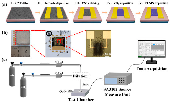
Figure 1.
(a) Fabrication process flow diagram, (b) a typically fabricated chip, and (c) schematic diagram of the gas-sensing measurement setup.
The morphologies of the CNTs and VO2 films were observed via field-emission scanning electron microscopy (FE-SEM, Sigma500, ZEISS, Oberkochen, Germany). The purity of the CNTs film was studied with a UV–vis–NIR spectrophotometer (UV-3600, Shimadzu, Kyoto, Japan). The defect degree of the CNT film and the molecular structure of the Pd@VO2 material were studied via Raman spectroscopy (Renishaw, Wotton-under-Edge, UK). The chemical composition of the material was characterized via energy-dispersive X-ray spectroscopy (EDS). The composition of VO2 was analyzed via X-ray diffraction (XRD, Rigaku D/Max 2500 PC, Bruker, Mannheim, Germany). The surface composition and chemical state were studied via X-ray photoelectron spectroscopy (XPS, Thermo escalab 250 Xi, Thermo Fisher Scientific, Waltham, MA, USA) using an Al Kα excitation source. The electrical properties of the CNTs-based TFT were measured using a Keithly 4200 semiconductor analyzer and a probe station (Cascade Microtech MPS 150, Tektronix, Beaverton, OR, USA). In order to measure the gas-sensing properties, the as-prepared sensor was assembled on a self-made PCB board via wire bonding, as shown in Figure 1b. The performance of the gas sensor was measured on a CGS-MT intelligent gas sensitivity analysis system (Beijing Elite Technology Co., Ltd., Beijing, China), as shown in Figure 1c. Usually, sensitivity is defined as the ratio of sensor response to gas concentration [31]. The response can be defined as (Ia−Ig)/Ia × 100(%), where Ia and Ig are the current of the sensor in air and the target gas, respectively [32].
3. Results and Discussion
TFT-type sensors take advantage of CNTs as the channel material and then utilize Pd@VO2-modified CNTs as the sensitive material to capture CH4. Therefore, high-semiconductor purity CNT films and pure Pd@VO2 materials without other impurities are the fundamental guarantee for realizing the sensitive detection of CH4 [29,30]. In order to study the morphology, purity, and defects of the CNT film, FE-SEM images, UV–vis–NIR absorption spectra, and Raman spectra are obtained. The SEM image in Figure S1 shows a randomly oriented and uniform CNT film [33], which laid the foundation for the fabrication of a TFT gas sensor with high sensitivity [10]. Figure 2a shows the absorption spectra of the CNT film in the range of 400–1500 nm. The existence of the M11 peak (located between 600 and 800 nm) and the sharp S22 peak (located at 820–1350 nm) indicates that the CNT film had with high semiconductor purity, which is a prerequisite to ensure the successful preparation of CNTs-based FET sensors [26]. According to the experimental relationship of ω = 248/d (nm), the radial breathing mode (RBM) peak (Figure 2b) at 168 cm−1 indicated that the diameter of the CNTs was distributed around 1.5 nm [10]. The high IG/ID ratio indicated that the CNTs used in this work exhibited fewer defects, which explained the subsequent modification of the CNTs film. In addition, the symmetrical Lorentz-type G peak indicated the semiconductor nature of the CNTs, which is consistent with the results obtained via absorption spectrum (Figure 2a). In order to determine the distribution and composition of the VO2 and Pd materials, FE-SEM images, EDS spectra, XRD patterns, Raman spectra, and XPS spectra were obtained. Figure S2 depicts an SEM image of Pd@VO2, and the inset shows an FE-SEM image at high magnification. It can be seen that the material produced via inkjet printing had a more uniform distribution, which is conducive to the uniform diffusion of gas molecules on the surface [34]. At high magnification, the diameter of the VO2 nanoparticles could be estimated to be about 100–200 nm, but the Pd nanoparticles could not be well observed in the SEM image due to their small amount. In order to verify the presence of Pd nanoparticles, EDS analysis was carried out. In addition to the V and O, Si could be seen in the EDS spectrum; Pd could also be observed, as shown in Figure 2c, which confirmed the existence of Pd in the Pd@VO2 composites [35]. The spectrum shows that there were no other impurities in the sample (the Si element’s peak originated from the silicon substrate). The EDS mapping in Figure S3a–c also shows the uniform element distribution in each part of the material, which is consistent with the above SEM results. Figure 2d shows the XRD spectra of the Pd@VO2 and VO2 materials. It can be seen that there was no change after Pd modification, and all the diffraction peaks in the XRD spectra corresponded to monoclinic VO2 (PDF#44-0252) [36,37]. No other phase or impurity peaks were detected in the XRD spectra, further indicating the high purity of the material prepared in this work. In order to investigate the molecular structure of the as-prepared material, the Raman spectra of VO2 and Pd@VO2 were measured, as depicted in Figure 2e. It can be seen that there was no change in the Raman spectrum of VO2 after the modification with Pd nanoparticles. The five peaks at 140 cm−1, 282 cm−1, 408 cm−1, 691, and 991 cm−1 correspond to the fundamental modes of VO2 monoclinic crystal, which is consistent with the results of XRD patterns. The two peaks at 140 cm−1 and 187 cm−1 are strongly consistent with a layered structure. The other peaks at 282 cm−1 and 408 cm−1 are the bending vibration bonds of V=O. The peak at 691 cm−1 conforms to the double oxygen (V-O-V) stretching mode, which is formed by the sharing of oxygen at the corners of two pyramids. The high long-shift peak at 991 cm−1 is consistent with the tensile vibration of terminal oxygen (V=O) [38,39,40]. The surface chemical state of Pd@VO2 was further determined via XPS measurements. The XPS spectra in Figure 2f prove the presence of V, O, and Pd elements, and the C 1s peak was used for charge correction [41]. The O 1s peak (~530.2 eV) and Pd 3p3/2 peak (532.9 eV) can be observed from Figure 2g. The Pd 3p3/2 peak, Pd 3d3/2 peak (341.5 eV), and Pd 3d5/2 peak (336.2 eV) in Figure 2i proved that the existence of Pd in the form of an elementary substance [42], which guaranteed the catalytic effect during the subsequent gas-sensing reaction. In the spectra in Figure 2h, the two binding energies of 517 eV and 515.9 eV obtained in the V 2p3/2 environment belong to V5+ and V4+, respectively. The large amount of V5+ may have been due to the easy oxidation of vanadium in contact with air during the gas-sensing test, so completely oxidized V5+ seems to be very common on the surface of vanadium-oxide materials [43].
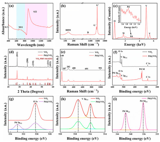
Figure 2.
Characterization of the CNTs, VO2, and Pd@VO2 thin film used for constructing gas sensors. The (a)UV−vis−NIR absorption spectrum and the (b) Raman spectrum of the CNT film. (c) EDS, (d) XRD patterns, (e) Raman spectra, and (f) XPS full spectra of VO2 and Pd@VO2. (g–i) Fine spectra obtained by narrow a-rea scanning of Pd@VO2.
As a platform utilized for the detection of CH4, CNTs-based TFT sensors should be reliable and uniform. CNTs-based TFT sensors were tested using a common source approach with gate voltages ranging from −60 V to +60 V and a fixed drain-source voltage of −0.1 V. The randomly selected unmodified CNTs-based TFT sensors exhibited highly uniform transfer characteristic curves with small changes (Figure 3a). All transistors exhibited p-type FET characteristics [44], and the current on/off ratio was calculated to be greater than 104, which is crucial for charge transport and reliable detection. In order to compare the effect of VO2, Pd, and Pd@VO2 modification, the corresponding transfer characteristic curves of the modified CNTs-based TFT sensors were also tested (Figure 3b). Compared with the unmodified TFT, the VO2 material deposited on TFT did not change the transfer characteristic curve. However, the threshold voltage of CNTs modified with Pd generated significant drift due to the strong shielding effect of Pd nanoparticles [12]. For the Pd@VO2 TFT sensor, the transfer characteristic curve of TFT showed a significant horizontal shift, which was caused by the change in the work function of the sensitive materials [45]. The gas-sensing properties of CNTs-based TFT sensors modified with VO2 and Pd@VO2 were further investigated. All the sensing measurements in this work were recorded at Vds = −0.1 V and Vgs-backgate = 0 V, working at room temperature. In order to explore the optimal temperature of the sensor, the Pd@VO2 TFT sensor was measured at different temperatures from room temperature (25 °C) to 100 °C. It can be seen from Figure 4a that the Pd@VO2 TFT sensor demonstrated the strongest response at room temperature. With the increase in temperature, VO2 is oxidized to V2O3 and V2O5, which leads to the decrease in the response of the sensor [46]. Figure 4b shows the transient response of the CNTs-based sensors modified with VO2 and Pd@VO2 to 50–500 ppm CH4 at room temperature. It can be clearly observed that the response of the Pd@VO2 TFT sensor increased sharply when CH4 was introduced, while the VO2 TFT sensor had almost no response to CH4 in the concentration range from 50 to 200 ppm. Noticeably, the TFT sensors presented comparatively regular baseline drift during the gas-sensing test cycles. Baseline drift is typical for the metal–oxide-based gas sensors, which is normally attributed to surface atomic rearrangement [47]. Additionally, the regular baseline drift seems to be an inevitable phenomenon for Pd@VO2 TFT gas sensors, which can be handled by the back-end circuit in future practical applications. Because the response reflects the relative change in current, the baseline drift has relatively little interference on gas-sensing detection. Figure S4 shows the two-cycle response–recovery curve of the Pd-modified CNT sensor toward 500 ppm CH4. After CH4 was introduced, the current of the sensor did not change, indicating that the Pd modified CNTs-based sensor was not sensitive to CH4. This further confirmed that Pd only plays a catalytic role in the sensor. Figure 4c plots the fitting curves of the VO2 TFT sensor and Pd@VO2 TFT sensor at the CH4 test concentration. It can be seen that the experimental limits of detection (LODs) of the VO2 TFT sensor and Pd@VO2 TFT sensor were 300 ppm and 50 ppm, respectively. According to the theoretical calculation formula (LOD (ppm) = 3 × RMSnoise/Slope) [48], Pd@VO2 and VO2 TFT sensors can achieve detection limits of 25 ppm and 195 ppm, respectively. Moreover, the sensitivities of the Pd@VO2 and VO2 TFT sensors were calculated to be 0.698% ppm−1 and 0.273% ppm−1, respectively. Therefore, Pd modification not only improves the detection limit of the sensor for CH4 but also improve the sensitivity. Figure 4d depicts the dynamic response of the sensor to 500 ppm CH4 working at room temperature. After the sensor was exposed to 500 ppm CH4 for 30 min to record the sensing signal, the sensor was exposed to a clean air flow for 30 min again to recover the sensor, and four such cycles were repeated. The incomplete recyclability could be ascribed to the fact that the desorption energy required for gas desorption is difficult to be satisfied at room temperature. The sensing behavior of the VO2 and Pd@VO2 TFT sensors seemed to be quite repeatable. It can also be clearly seen from Figure 4e that the Pd@VO2 TFT sensor had a stronger response to CH4 than the VO2 TFT sensor. From the responses of the two sensors to CH4 shown in Figure 4e, it could be calculated that the response of Pd@VO2 TFT sensor was about five times than that of the VO2 TFT sensor. This enhancement could be attributed to the Pd nanoparticles catalyzing the dissociation and adsorption of CH4 and oxygen molecules via the spillover effect [2], which then facilitates the adsorption of CH4 and increases the electronic interaction with CNTs, which leads to the reduction in CNTs carriers and makes the sensor more responsive. In addition, the selectivity of a gas sensor is an important parameter in practical applications. The selectivity of the Pd@VO2 TFT sensor to CH4 was compared by contacting different gases of SO2, CO, benzene, and CH4, which are common gases in coal mines and kitchens. Figure 4e shows the selectivity histogram of the Pd@VO2 TFT sensor at room temperature, and the selectivity to a specific gas is defined as Sspecific gas/Sinterference gas [49]. Compared with CH4, the selectivity to SO2, CO, and benzene was about 49%, 26%, and 39%, respectively. Although the selectivity of the Pd@VO2 TFT sensor to methane is not satisfactory, the 50 ppm methane is far below the lower explosive limit, and the concentration of other interfering gases in the coal mine environment is even lower, so the Pd@VO2 TFT sensor might show better and relatively ideal selectivity in practical applications. In addition, the Pd@VO2 TFT sensor was stored in ambient air without power, and the sensor was discontinuously tested several times within 25 days, with each exposure being to 500 ppm CH4 for 30 min. The long-term stability evaluation of the CH4 sensor for 500 ppm CH4 is shown in Figure 4f. It is clearly seen that the response value and initial current of the CH4 sensor maintained excellent consistency without significant decay over 25 days. In addition, the moisture resistance of the sensor was further examined under different relative humidity values (0%, 10%, 30%, 50%, 70%, and 90%) at room temperature (data not shown). It was found that the humidity had a great influence on the sensor, especially when working at high humidity conditions, which is a problem to be solved for the gas sensors currently operating at room temperature. We will focus on solving the inferior humidity resistance in future work.
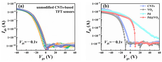
Figure 3.
Electrical properties of TFT sensors. (a) Transfer characteristic curves of the randomly selected unmodified CNTs-based TFT sensors. (b) Comparison of transfer characteristic curves of VO2, Pd, and Pd@VO2 TFT sensors with those of unmodified sensor.
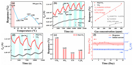
Figure 4.
Gas-sensing properties of TFT sensors. (a) The response values of Pd@VO2 TFT sensor toward 500 ppm CH4 at different working temperatures. (b) The dynamic response–recovery curves, (c) the fitted curves, (d) the reproducibility test curves, and (e) the response values of Pd@VO2 TFT sensor toward different gases at 50 ppm. (f) The response value and base current change in Pd@VO2 TFT sensor measured several times within 25 days.
Based on the analysis of the above results, the main reason for the in of the gas sensitivity of the Pd@VO2 TFT-type sensor may be attributed to the catalytic effect of Pd modification [2,50], which promotes the electronic interaction between CH4 and gas-sensing materials and then regulates the CNTs’ electronic transmission channel. In addition, the inkjet printing method was used to make the sensitive material uniformly modify onto the surface of a CNT film, which is conducive to the uniform diffusion of gas molecules on a gas-sensing material surface [34]. The TFT gas-sensing platform based on CNTs modified by Pd@VO2 is illustrated in Figure 5a. In air, the oxygen molecules adsorbed on the surface of VO2 capture electrons from VO2-CNTs to form O2- [51]. Therefore, the carriers of the p-type semiconductor CNTs increase instead, resulting in the widening of the conductive channel of the CNTs. In a CH4 atmosphere, the generated electrons are released to VO2-CNTs due to the redox reaction between CH4 molecules and oxygen ions, so that the carriers of p-type semiconducting CNTs are reduced, resulting in the narrowing of the conductive channel of the CNTs. Due to the insufficient activation energy between the CH4 and oxygen ions, the feeble redox reaction rate ultimately results in inferior gas-sensing properties of a sensor when operating at room temperature. It is noteworthy that Pd, as an active noble metal, can catalyze the dissociative adsorption of CH4 and oxygen molecules via the spillover effect [52,53]. After the modification of Pd nanoparticles, Pd can promote the dissociation of oxygen molecules to produce oxygen atoms, which then spill over to the VO2 surface and capture electrons from VO2-CNTs to form oxygen ions. The process can increase the adsorption amount of oxygen and the molecule–ion conversion rate of oxygen to provide more active sites for CH4 gas (Figure 5b) [52]. In a CH4 atmosphere, Pd can reduce the activation energy of the redox reaction between CH4 and oxygen ions and can promote the dissociation of C-H bonds in CH4 to form CH3 and H [52]. The reaction is as follows [2]:
Subsequently, CH3 and H spill onto the VO2 surface and react with the preadsorbed oxygen ions to generate more free electrons (Figure 5c). The reaction is as follows [49]:
Finally, the CNTs’ conductive channels become narrower, which leads to the improvement in the gas-sensing properties of Pd@VO2 TFT sensors. In other words, the use of CNTs as the conductive channel of the TFT and the Pd@VO2 composite as the sensitive layer of the sensor to capture CH4 molecules seems to be the key factors to ultimately improving the gas-sensing properties of CNTs-based TFT gas sensors.
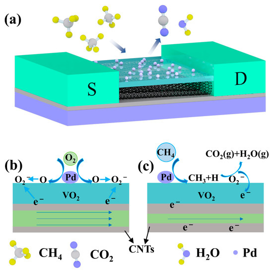
Figure 5.
(a) Pd@VO2 TFT gas-sensing platform based on CNTs. Schematic illustrations of the gas-sensing mechanisms (b) in air and (c) in CH4 gas.
4. Conclusions
In summary, a TFT-type gas sensor based on a CNT film was successfully fabricated by using semiconductor processing technology. Specifically, VO2 material was deposited on the top of the semiconductor CNT channel via inkjet printing to achieve the detection of CH4 at room temperature. Then, Pd nanoparticles as the catalyst were deposited onto the surface of the VO2 material; finally, the Pd@VO2 TFT sensor showed better CH4-sensing properties. The response of the Pd@VO2 TFT sensor toward 500 ppm CH4 was about five times than that of the VO2 TFT sensor under the same conditions, and the detection limit was optimized from 300 ppm to 50 ppm. The detection of CH4 at room temperature could be attributed to the redox reaction of VO2 nanomaterials, and the improvement in the gas-sensing performance of the Pd@VO2 TFT sensor could be ascribed to the spillover effect of Pd nanoparticles. Our work provides a valuable reference for the low power consumption, miniaturization, and integrability of gas sensors, which opens a new window for the integration of high-performance micro gas sensors into electronic equipment.
Supplementary Materials
The following supporting information can be downloaded at: https://www.mdpi.com/article/10.3390/chemosensors11070365/s1, Figure S1: FE-SEM image of the CNTs. Figure S2: FE-SEM image of Pd@VO2, and the inset shows FE-SEM image at high magnification. Figure S3: EDS mapping of elements (a) V, (b) O, and (c) Pd. Figure S4: Two-cycle test of Pd-modified CNTs sensor for 500 ppm CH4 at room temperature.
Author Contributions
Conceptualization, Y.Z.; methodology, F.J.; validation, F.J.; investigation, F.J.; writing—original draft preparation, F.J.; writing—review and editing, J.H. and Y.Z.; supervision, J.H. and Y.Z.; funding acquisition, J.H. and Y.Z. All authors have read and agreed to the published version of the manuscript.
Funding
This research was funded by National Natural Science Foundation of China, grant numbers 62071410 and 62101477; and the Hunan Provincial Natural Science Foundation of China, grant number 2021JJ40542.
Institutional Review Board Statement
Not applicable.
Informed Consent Statement
Not applicable.
Data Availability Statement
Data are available from the authors under reasonable request.
Conflicts of Interest
The authors declare no conflict of interest.
References
- Chimowa, G.; Tshabalala, Z.P.; Akande, A.A.; Bepete, G.; Mwakikunga, B.; Ray, S.S.; Benecha, E.M. Improving CH4 gas sens-ing properties of multi-walled carbon nanotubes by vanadium oxide filling. Sens. Actuators B Chem. 2017, 247, 11–18. [Google Scholar] [CrossRef]
- Wang, Y.; Meng, X.; Yao, M.; Sun, G.; Zhang, Z. Enhanced CH4 sensing properties of Pd modified ZnO nanosheets. Ceram. Int. 2019, 45, 13150–13157. [Google Scholar] [CrossRef]
- Liang, J.; Liu, J.; Li, N.; Li, W. Magnetron sputtered Au-decorated vanadium oxides composite thin films for CH4-sensing properties at room temperature. J. Alloys Compd. 2016, 671, 283–290. [Google Scholar] [CrossRef]
- Liang, J.; Li, W.; Liu, J.; Hu, M. Room temperature CH4 sensing properties of Au decorated VO2 nanosheets. Mater. Lett. 2016, 184, 92–95. [Google Scholar] [CrossRef]
- Kim, W.-T.; Kim, I.-H.; Choi, W.-Y. Fabrication of TiO2 Nanotube Arrays and Their Application to a Gas Sensor. J. Nanosci. Nanotechnol. 2015, 15, 8161–8165. [Google Scholar] [CrossRef] [PubMed]
- Zhang, Y.; Li, Y.; Liu, W.; Li, F.; Zhan, Z. Design of SnO2-based CH4 sensors with reactive anti-poisoning layers: Excellent stability and high resistance to hexamethyldisiloxane. J. Mater. Sci. 2023, 58, 2140–2155. [Google Scholar] [CrossRef]
- Sun, Y.; Hu, J.; Zhang, Y. Visible light assisted trace gaseous NO2 sensor with anti-humidity ability via LSPR enhancement effect. Sens. Actuators B Chem. 2022, 367. [Google Scholar] [CrossRef]
- Lu, G.; Ocola, L.E.; Chen, J. Room-Temperature Gas Sensing Based on Electron Transfer between Discrete Tin Oxide Nano-crystals and Multiwalled Carbon Nanotubes. Adv. Mater. 2009, 21, 2487–2491. [Google Scholar] [CrossRef]
- Hu, J.; Liu, X.; Zhang, J.; Gu, X.; Zhang, Y. Plasmon-activated NO2 sensor based on Au@MoS2 core-shell nanoparticles with heightened sensitivity and full recoverability. Sens. Actuators B Chem. 2023, 382, 133505. [Google Scholar] [CrossRef]
- Xiao, M.; Li, Y.; Zhang, B.; Sun, G.; Zhang, Z. Synthesis of g-C3N4-Decorated ZnO Porous Hollow Microspheres for Room-Temperature Detection of CH4 under UV-Light Illumination. Nanomaterials 2019, 9, 1507. [Google Scholar] [CrossRef]
- Xiao, M.; Liang, S.; Han, J.; Zhong, D.; Liu, J.; Zhang, Z.; Peng, L. Batch Fabrication of Ultrasensitive Carbon Nanotube Hydro-gen Sensors with Sub-ppm Detection Limit. ACS Sens. 2018, 3, 749–756. [Google Scholar] [CrossRef] [PubMed]
- Liu, F.; Xiao, M.; Ning, Y.; Zhou, S.; He, J.; Lin, Y.; Zhang, Z. Toward practical gas sensing with rapid recovery semiconducting carbon nanotube film sensors. Sci. China Inf. Sci. 2022, 65, 162402. [Google Scholar] [CrossRef]
- Abd, I.K.; Shano, A.M.; Khodair, Z.T. MWCNT Thin Films by CVD Method and Some Applications. J. Nano-Electron. Phys. 2022, 14, 06002. [Google Scholar] [CrossRef]
- Shukla, P.; Saxena, P.; Madhwal, D.; Bhardwaj, N.; Jain, V.K. Electrostatically functionalized CVD grown multiwalled carbon nanotube/palladium polymer nanocomposite (MWCNT/Pd) for CH4 detection at room temperature. Chem. Eng. Sci. 2022, 264, 118191. [Google Scholar] [CrossRef]
- Lu, Y.; Li, J.; Han, J.; Ng, H.T.; Binder, C.; Partridge, C. Meyyappan, room temperature CH4 detection using palladium loaded single-walled carbon nanotube sensors. Chem. Phys. Lett. 2004, 391, 344–348. [Google Scholar] [CrossRef]
- Aroutiounian, V.M. Metal oxide gas sensors decorated with carbon nanotubes. Lith. J. Phys. 2015, 55, 4. [Google Scholar] [CrossRef]
- Afrin, R.; Shah, N. Room temperature gas sensors based on carboxyl and thiol functionalized carbon nanotubes buckypapers. Diam. Relat. Mater. 2015, 60, 42–49. [Google Scholar] [CrossRef]
- Humayun, T.; Divan, R.; Liu, Y.; Gundel, L.; Solomon, P.A.; Paprotny, I. Novel chemoresistive CH4 sensor with 10 ppm sensitivity based on multiwalled carbon nanotubes functionalized with SnO2 nanocrystals. J. Vac. Sci. Technol. A 2016, 34, 01A131. [Google Scholar] [CrossRef]
- Humayun, M.T.; Divan, R.; Stan, L.; Gupta, A.; Rosenmann, D.; Gundel, L.; Solomon, P.A.; Paprotny, I. ZnO functionalization of multiwalled carbon nanotubes for CH4 sensing at single parts per million concentration levels. J. Vac. Sci-Ence Technol. B Nanotechnol. Microelectron. Mater. Process. Meas. Phenom. 2015, 33, 06FF01. [Google Scholar]
- Chen, C.; Jiang, M.; Luo, X.; Tai, H.; Jiang, Y.; Yang, M.; Xie, G.; Su, Y. Ni-Co-P hollow nanobricks enabled humidity sensor for respiratory analysis and human-machine interfacing. Sens. Actuators B Chem. 2022, 370, 132441. [Google Scholar] [CrossRef]
- Prasad, A.K.; Amirthapandian, S.; Dhara, S.; Dash, S.; Murali, N.; Tyagi, A.K. Novel single phase vanadium dioxide nanostructured films for CH4 sensing near room temperature. Sens. Actuators B Chem. 2014, 191, 252–256. [Google Scholar] [CrossRef]
- Li, W.; Liang, J.; Liu, J.; Zhou, L.; Yang, R.; Hu, M. Synthesis and room temperature CH4 gas sensing properties of vanadium dioxide nanorods. Mater. Lett. 2016, 173, 199–202. [Google Scholar] [CrossRef]
- Chen, Y.; Zhang, W.; Luo, N.; Wang, W.; Xu, J. Defective ZnO Nanoflowers Decorated by Ultra-Fine Pd Clusters for Low-Concentration CH4 Sensing: Controllable Preparation and Sensing Mechanism Analysis. Coatings 2022, 12, 677. [Google Scholar] [CrossRef]
- Li, S.; Huang, H.; Zhao, D. GaN Nanowires Decorated with Pd for CH4 Gas Sensor. In IOP Conference Series: Earth and Envi-ronmental Science; IOP Publishing: Bristol, UK, 2020; p. 042037. [Google Scholar]
- Luo, S.; Chen, R.; Wang, J.; Xiang, L. ZnO/Pd@ ZIF-7-Based Gas Sensors for Selective CH4 Sensing. ACS Appl. Nano Mate-Rials 2023, 67, 5808–5816. [Google Scholar] [CrossRef]
- Liu, C.; Hu, J.; Wu, G.; Cao, J.; Zhang, Z.; Zhang, Y. Carbon Nanotube-Based Field-Effect Transistor-Type Sensor with a Sens-ing Gate for Ppb-Level Formaldehyde Detection. ACS Appl. Mater. Interfaces 2021, 13, 56309–56319. [Google Scholar] [CrossRef]
- Kim, C.-H.; Cho, I.-T.; Shin, J.-M.; Choi, K.-B.; Lee, J.-K.; Lee, J.-H. A New Gas Sensor Based on MOSFET Having a Horizontal Floating-Gate. IEEE Electron Device Lett. 2013, 35, 265–267. [Google Scholar] [CrossRef]
- Hong, Y.; Kim, C.-H.; Shin, J.; Kim, K.Y.; Kim, J.S.; Hwang, C.S.; Lee, J.-H. Highly selective ZnO gas sensor based on MOSFET having a horizontal floating-gate. Sens. Actuators B Chem. 2016, 232, 653–659. [Google Scholar] [CrossRef]
- Liang, Y.; Xiao, M.; Wu, D.; Lin, Y.; Liu, L.; He, J.; Zhang, G.-J.; Peng, L.-M.; Zhang, Z. Wafer-Scale Uniform Carbon Nanotube Transistors for Ultrasensitive and Label-Free Detection of Disease Biomarkers. ACS Nano 2020, 14, 8866–8874. [Google Scholar] [CrossRef]
- Zhou, S.; Xiao, M.; Liu, F.; He, J.; Lin, Y.; Zhang, Z. Sub-10 parts per billion detection of hydrogen with floating gate transis-tors built on semiconducting carbon nanotube film. Carbon 2021, 180, 41–47. [Google Scholar] [CrossRef]
- Franco, M.A.; Conti, P.P.; Andre, R.S.; Correa, D.S. A review on chemiresistive ZnO gas sensors. Sens. Actuators Rep. 2022, 4, 100100. [Google Scholar] [CrossRef]
- Huang, Y.; Guo, J.; Kang, Y.; Ai, Y.; Li, C.M. Two dimensional atomically thin MoS2 nanosheets and their sensing applica-tions. Nanoscale 2015, 7, 19358–19376. [Google Scholar] [CrossRef]
- Biswas, C.; Lee, S.Y.; Ly, T.H.; Ghosh, A.; Dang, Q.N.; Lee, Y.H. Chemically Doped Random Network Carbon Nanotube p–n Junction Diode for Rectifier. ACS Nano 2011, 5, 9817–9823. [Google Scholar] [CrossRef]
- Peng, X.; Liu, J.; Tan, Y.; Mo, R.; Zhang, Y. A CuO thin film type sensor via inkjet printing technology with high reproducibil-ity for ppb-level formaldehyde detection. Sens. Actuators B Chem. 2022, 362, 131775. [Google Scholar] [CrossRef]
- Braun, F.; Tarditi, A.M.; Miller, J.B.; Cornaglia, L.M. Pd-based binary and ternary alloy membranes: Morphological and perm-selective characterization in the presence of H2S. J. Membr. Sci. 2014, 450, 299–307. [Google Scholar] [CrossRef]
- Alie, D.; Gedvilas, L.; Wang, Z.; Tenent, R.; Engtrakul, C.; Yan, Y.; Shaheen, S.E.; Dillon, A.C.; Ban, C. Direct synthesis of ther-mochromic VO2 through hydrothermal reaction. J. Solid State Chem. 2014, 212, 237–241. [Google Scholar] [CrossRef]
- Kong, F.; Li, M.; Pan, S.; Zhang, Y.; Li, G. Synthesis and thermal stability of W-doped VO2 nanocrystals. Mater. Res. Bull. 2011, 46, 2100–2104. [Google Scholar] [CrossRef]
- Chen, L.; Ruan, Y.; Zhang, G.; Wei, Q.; Jiang, Y.; Xiong, T.; He, P.; Yang, W.; Yan, M.; An, Q.; et al. Ultrastable and High-Performance Zn/VO2 Battery Based on a Reversible Single-Phase Reaction. Chem. Mater. 2019, 31, 699–706. [Google Scholar] [CrossRef]
- Li, R.; Liu, C.-Y. VO2(B) nanospheres: Hydrothermal synthesis and electrochemical properties. Mater. Res. Bull. 2010, 45, 688–692. [Google Scholar] [CrossRef]
- Lee, S.-H.; Cheong, H.M.; Seong, M.J.; Liu, P.; Tracy, C.; Mascarenhas, A.; Pitts, J.; Deb, S.K. Raman spectroscopic studies of amorphous vanadium oxide thin films. Solid State Ion. 2003, 165, 111–116. [Google Scholar] [CrossRef]
- Silversmit, G.; Depla, D.; Poelman, H.; Marin, G.B.; De Gryse, R. Determination of the V2p XPS binding energies for different vanadium oxidation states (V5+ to V0+). J. Electron Spectrosc. Relat. Phenom. 2004, 135, 167–175. [Google Scholar] [CrossRef]
- Brun, M.; Berthet, A.; Bertolini, J. XPS, AES and Auger parameter of Pd and PdO. J. Electron Spectrosc. Relat-Ed Phenom. 1999, 104, 55–60. [Google Scholar] [CrossRef]
- Powell, M.J.; Godfrey, I.J.; Quesada-Cabrera, R.; Malarde, D.; Teixeira, D.; Emerich, H.; Palgrave, R.G.; Carmalt, C.J.; Parkin, I.P.; Sankar, G. Qualitative XANES and XPS Analysis of Substrate Effects in VO2 Thin Films: A Route to Improving Chemical Vapor Deposition Synthetic Methods? J. Phys. Chem. C 2017, 121, 20345–20352. [Google Scholar] [CrossRef]
- Luo, M.; Zhu, M.; Wei, M.; Shao, S.; Robin, M.; Wei, C.; Cui, Z.; Zhao, J.; Zhang, Z. Radiation-hard and repairable complemen-tary metal–oxide–semiconductor circuits integrating n-type indium oxide and p-type carbon nanotube field-effect transis-tors. ACS Appl. Mater. Interfaces 2020, 12, 49963–49970. [Google Scholar] [CrossRef] [PubMed]
- Zhang, Z.; Wang, S.; Ding, L.; Liang, X.; Pei, T.; Shen, J.; Xu, H.; Chen, Q.; Cui, R.; Li, Y.; et al. Self-Aligned Ballistic n-Type Single-Walled Carbon Nanotube Field-Effect Transistors with Adjustable Threshold Voltage. Nano Lett. 2008, 8, 3696–3701. [Google Scholar] [CrossRef]
- Xu, X.; He, X.; Wang, G.; Yuan, X.; Liu, X.; Huang, H.; Chu, J. The study of optimal oxidation time and different tempera-tures for high quality VO2 thin film based on the sputtering oxidation coupling method. Appl. Surf. Sci. 2011, 257, 8824–8827. [Google Scholar] [CrossRef]
- Bertrand, J. Spectroscopic and Electrical Studies of the Influence of Electrodes on SnO2 Based Sensors. Ph.D. Thesis, Tübingen, Univ., Tübingen, Germany, 2008. [Google Scholar]
- Liu, J.; Hu, Z.; Zhang, Y.; Li, H.-Y.; Gao, N.; Tian, Z.; Zhou, L.; Zhang, B.; Tang, J.; Zhang, J.; et al. MoS2 Nanosheets Sensitized with Quantum Dots for Room-Temperature Gas Sensors. Nano-Micro Lett. 2020, 12, 219–242. [Google Scholar] [CrossRef]
- Kim, S.-J.; Hwang, I.-S.; Kang, Y.C.; Lee, J.-H. Design of Selective Gas Sensors Using Additive-Loaded In2O3 Hollow Spheres Prepared by Combinatorial Hydrothermal Reactions. Sensors 2011, 11, 10603–10614. [Google Scholar] [CrossRef] [PubMed]
- Horastani, Z.K.; Sayedi, S.M.; Sheikhi, M.H.; Rahimi, E. Effect of silver additive on electrical conductivity and CH4 sensitivity of SnO2. Mater. Sci. Semicond. Process. 2015, 35, 38–44. [Google Scholar] [CrossRef]
- Mounasamy, V.; Mani, G.K.; Madanagurusamy, S. Vanadium oxide nanostructures for chemiresistive gas and vapour sens-ing: A review on state of the art. Microchim. Acta 2020, 187, 253. [Google Scholar] [CrossRef]
- Nasresfahani, S.; Sheikhi, M.; Tohidi, M.; Zarifkar, A. CH4 gas sensing properties of Pd-doped SnO2/reduced graphene oxide synthesized by a facile hydrothermal route. Mater. Res. Bull. 2017, 89, 161–169. [Google Scholar] [CrossRef]
- Liu, C.; Suematsu, K.; Uchiyama, A.; Watanabe, K.; Guo, Y.; Wang, D.; Shimanoe, K. Impact of Pd nanoparticle loading meth-od on SnO2 surface for natural gas detection in humid atmosphere. J. Mater. Sci. 2021, 56, 13975–13988. [Google Scholar] [CrossRef]


Disclaimer/Publisher’s Note: The statements, opinions and data contained in all publications are solely those of the individual author(s) and contributor(s) and not of MDPI and/or the editor(s). MDPI and/or the editor(s) disclaim responsibility for any injury to people or property resulting from any ideas, methods, instructions or products referred to in the content. |
© 2023 by the authors. Licensee MDPI, Basel, Switzerland. This article is an open access article distributed under the terms and conditions of the Creative Commons Attribution (CC BY) license (https://creativecommons.org/licenses/by/4.0/).