Article

A Simple Method to Fabricate the Highly Sensitive SERS Substrate by Femtosecond Laser-Based 3D Printer

1
Department of Biomechatronic Engineering, College of Biotechnology and Bioengineering, Sungkyunkwan University, Suwon 16419, Republic of Korea
2
Holonyak Micro and Nanotechnology Lab, University of Illinois at Urbana and Champaign, Urbana, IL 61801, USA
3
College of AI Convergence, Chonnam National University, Gwangju 61186, Republic of Korea
4
Korea Institute of Medical Microrobotics, Gwangju 61011, Republic of Korea
5
Department of Electrical Engineering, Korea National University of Transportation, Chungju 27469, Republic of Korea
*
Authors to whom correspondence should be addressed.
These authors contributed equally to this work.
Chemosensors 2023, 11(6), 340; https://doi.org/10.3390/chemosensors11060340
Submission received: 18 May 2023 / Revised: 4 June 2023 / Accepted: 6 June 2023 / Published: 8 June 2023
(This article belongs to the Special Issue Chemosensors in Biological Challenges)

Abstract

:
Surface-enhanced Raman spectroscopy (SERS) is a potent technique for analyzing and detecting various targets, including toxic ions, pesticides, and biomarkers, at the single-molecule level. The efficiency of SERS techniques relies heavily on the underlying SERS substrate, which is primarily responsible for the strong induction of localized plasmon resonance on nanostructures. Noble metals such as gold and silver were commonly used to fabricate SERS substrates, leveraging the electromagnetic mechanism (EM) to enhance the Raman signal. However, chemically synthesized nanoparticle-based SERS substrates suffer from low uniformity and reproducibility. Furthermore, the high cost associated with noble metals makes most SERS substrates expensive to produce. In this study, we present a straightforward method for fabricating a highly uniform and reproducible SERS substrate using a femtosecond laser-based 3D printer. Notably, our method offers good cost competitiveness since it requires only a minimal amount of gold coating for the SERS signal. Moreover, the proposed method exhibits exceptional versatility in SERS analysis and detection, catering to numerous targets in the field.

1. Introduction

Surface-enhanced Raman spectroscopy (SERS) is a powerful analytical technique that is widely used for the analysis of molecules at ultra-low concentrations, even down to a single molecule [1,2,3,4]. The SERS technique is induced from the metal surface, which can create a strong surface Plasmon resonance between the metal nano-gaps. The original Raman signal of a target is weak in terms of discrimination; however, the surface Plasmon resonance intensifies the Raman signal of the target by several orders of magnitude. For this reason, the metal surface, which is used as a SERS substrate, is the key point that can decide the efficiency of SERS sensors [5,6,7]. In particular, noble metals such as gold and silver have been widely used in SERS techniques due to their unique optic properties such as (1) plasmonic enhancement, (2) high Raman-scattering efficiency, (3) chemical stability, and (4) facile functionalization and fabrication. A gold or silver surface with numerous nano-gaps in structure makes SERS a versatile tool with a wide range of applications, including sensing, bio-imaging, and the identification of trace amounts of chemicals [8,9,10,11]. However, for the fabrication of the nano-gaps, chemical fabrication has mostly been used. The reason for this is that the fabrication of the nano-gaps between metal structures is difficult to intentionally manipulate. Due to the randomness of the chemical growth of nanostructures, the SERS substrate had chronic limitations in terms of uniformity.
Particularly, in the SERS techniques, the uniformity of the substrate is an important factor in surface-enhanced Raman spectroscopy (SERS), as it can affect the reproducibility and reliability of the results [3,4]. A uniform substrate can help to ensure that the SERS enhancement is consistent across the entire surface, which in turn can lead to more accurate and precise measurements [12,13]. A non-uniform substrate can result in variations in the SERS enhancement across the surface, which can lead to inconsistent or misleading results. Additionally, a non-uniform substrate can lead to difficulty in interpreting the SERS spectra, as it can be difficult to determine which peaks are arising from the analyte and which are arising from the substrate. For this reason, it is very important to choose a uniform substrate as the SERS substrate. As advanced 3D printing techniques have been developed, there have been attempts to make nanostructures using a femtosecond laser 3D printing system [14]. The femtosecond laser 3D printing system is a highly advanced and precise method for fabricating 3D structures at the micro- and nanoscale [14,15,16,17,18,19,20]. This method uses ultrashort laser pulses to precisely ablate material and build structures layer by layer, allowing for the creation of highly complex and uniform structures with a sub-micron resolution [21,22,23]. In the context of SERS, the femtosecond laser 3D printing system can be used to create highly uniform and homogeneous nano-pillar structures on the substrate, which can be important to ensure a consistent and high SERS signal [24,25]. Additionally, the precise control over the structures that can be achieved using the femtosecond laser 3D printing system can allow for further optimization of the SERS signal by controlling the diameters and distances of the nano-pillars [26,27].
In this study, a 3D printing technique was utilized to fabricate a uniform SERS substrate with nano-pillar structures. By controlling the radius of the nano-pillars, the SERS signal was optimized. The femtosecond laser 3D printing system was used to create uniform nano-pillar structures on the substrate, providing a platform for high-throughput SERS measurements. The uniformity and uniform distribution of the nano-pillars are important factors for ensuring a high and consistent SERS signal. By carefully controlling the radius of the nano-pillars, the local electromagnetic field was tailored to optimize the SERS signal for a given probe molecule. For optimization, we conducted an SERS analysis according to the various conditions controlling the printing speed and the pillar radius. Moreover, the differences between the coated metal, Ag/Cr coating, and Au/Cr coating on the 3D-printed SERS substrates were compared. This study aimed to demonstrate the potential of using 3D printing techniques to create uniform SERS substrates with nano-pillar structures and the optimization of the SERS signal achieved by controlling the diameters and distances of the nano-pillars. The results of this study have important implications for the development of high-throughput and ultra-sensitive SERS measurements for various applications in fields such as biology, chemistry, and material science.

2. Materials and Methods

2.1. Chemical Agents

All chemical reagents (sulphuric acid, hydrogen peroxide, isopropyl alcohol, ethanol, polydimethylsiloxane, and crystal violet) were purchased from Sigma-Aldrich (St. Louis, MO, USA). All the cover glasses (Paul Marienfeld GmbH & Co. KG, Lauda-Königshofen, Germany) were 10 mm in diameter and cleaned with piranha solution in concentrated sulphuric acid (98% w/v) and hydrogen peroxide (30% w/v) before use. All solutions were prepared using Millipore deionized water (DI water) with a resistivity of at least 18.2 MΩ cm at 25 °C.

2.2. Fabrication of Three-Dimensional Nanostructure by Femtosecond Laser 3D Printer

We used a femtosecond laser high-resolution 3D printer (Nanoscribe, Eggenstein-Leopoldshafen, Germany, Photonic Professional GT2) for fabricating 3D-printed nanostructures. We used a Dip-in Liquid Lithography mode (DiLL) for fabrication. For fabrication, a 63× objective lens, and IP-Dip photo-resin were used. The nanostructures we made are composed of a biocompatible and non-cytotoxic photo-resin (IP-Dip, Nanoscribe). After printing, the structures were washed using isopropyl alcohol and DI water). For optimization, we controlled the printing speed of the 3D printer from 5000 to 10,000 mm/s when printing nanostructures with different pillar radii. In addition, for optimization, the pillar radii of nanostructures were controlled to have 200, 400, 600, and 800 nm. The nanostructure with a pillar radius under 200 nm could not be fabricated due to the limitations of 3D printer resolution.
For the SERS application, we used the electron-beam evaporator (E-beam evaporator, ULTEC, UEE) for coating Au and Ag on the nanostructures. For better adhesion, chromium was used before Au- or Ag-coating in the same manner [28]. The 20 nm chrome, 80 nm Au, and 80 nm Ag were coated, respectively. All the sources were purchased from ULTEC. After coating Cr/Au or Cr/Ag on the substrates, the 3D-printed nanostructures were washed using ethanol and DI water.

2.3. SEM Analysis of 3D-Printed Nanostructure by Femtosecond Laser 3D Printer

The fabricated 3D-printed nanostructures were analyzed using a scanning electron microscope (SEM, Tescan, MIRA3, Brno, Czech). The morphology of the printed structure was observed by SEM at 5 kV.

2.4. SERS Analysis of 3D-Printed Nanostructure by Femtosecond Laser 3D Printer

For the SERS investigation of 3D-printed nanostructure by femtosecond laser 3D printer, 100 µM of crystal violet (CV) was treated on each substrate according to fabrication conditions. Before treating CV molecules, all the substrates were cleaned with DI water. A total of 2 µL of CV was dropped on the SERS substrate and dried for analysis.
All the 3D-printed nanostructures were analyzed with a Raman spectroscope (Renishaw inVia Raman Microscope) equipped with a 785 nm laser. Because we used the CV molecules (fluorescence dye) for investigation, the 785 nm laser is suitable for decreasing fluorescence interference. A 10× microscope lens (Leica DM2700M, DEU) and detector (Renishaw Centrus Detector, GBR) were used for analysis [1,29].
The surfaces were measured by five accumulations with a 1 s exposure (range: 700–1700 cm−1) at each point in the mapping area. To obtain SERS mapping images, Raman mapping sequences were conducted on the 3D-printed nanostructures. Each SERS mapping image contained over 100 spots. According to the fabrication conditions, all the samples were analyzed in the same manner.

3. Results and Discussion

3.1. Fabrication of 3D Nanostructure via Femtosecond Laser 3D Printer

For the facile fabrication of the 3D-printed nanostructure, we used a femtosecond laser system and ultra-high-resolution 3D printer. For the SERS substrate, the geometrical structures must have nano-gaps between them to efficiently amplifying the SERS signal. In addition to the high SERS intensity, it is crucial to have a uniform SERS substrate to ensure high reliability. In this sense, we fabricated 3D-printed nanostructures by controlling the pillar radius, which has different SERS efficiencies (Figure 1a). At first, with the 3D modeling program, we designed simple circular pillars with different radii. In detail, we considered three factors d (diameter), l (length), and p (distance between pillars). We set the l and p as 1000 nm. d represented controopen-accesse diameters from 200 nm to 800 nm. Depending on the radius, each pillar has different gaps and different SERS amplifying efficiencies. Therefore, the thin Au film and Cr film were coated on the 3D-printed nanostructures using the E-beam evaporator. Because it is well known that noble metals have a high SERS efficiency, attributed to the localized Plasmon surface resonance (LSPR) effect on the surface, Au and Ag were used to make SERS substrates.
Figure 1b shows photographic images of the 3D-printed nanostructures after Au/Cr coating with a 0.5 × 0.5 mm2 size. The yellow dotted box shows the magnified images. In the yellow dotted box, the slightly gray box shows the 3D printed nanostructures that were coated with the Au/Cr films. For the SERS investigation, we used the polydimethylsiloxane (PDMS) mold to treat the CV molecules on the substrate. Even though the femtosecond laser system has ultra-high-resolution 3D printing, it is still hard to recognize the 3D-printed nanostructure with the naked eye. This is because of the limitations of the computing system and the time consumption needed by the 3D printing to fabricate tiny spots. In Figure 1c,d, detailed images are shown with the cross stripes in the single 3D-printed nanostructures. Because of the computational limitations, we used an algorithm to extend the tiny circular pillar area. The tiny singular spot was composed of 25 × 25 µm2 size and has 625 circular pillars in the area. By the algorithm, the small single area was copied by 20 horizontally and vertically to expand the area. As a result, the total circular pillar was 250,000 in the 0.5 × 0.5 mm2 area, as shown in Figure 1c and Figure S1. In Figure 1d, grid patterns are visible even in the magnified image, in addition to the structural collapse (distortion) caused by printing structures that are too small.

3.2. Optimization of 3D Nanostructure via Femtosecond Laser 3D Printer

As mentioned earlier, uniformity is an important factor in the SERS substrate because it can determine the reliability. First, to obtain a high uniformity, we optimized the 3D-printed nanostructures by controlling the printing speed. By controlling the printing speed, we confirmed the microscopic images and SERS intensities according to the printing speed (Figure 2). Moreover, the 3D-printed SERS nanostructures were investigated, which were fabricated with different pillar radii ranging from 200 nm to 800 nm. By controlling the printing speed and pillar radius, we confirmed the optimized printing condition to obtain a higher SERS efficiency. In Figure 2a, the 3D-printed nanostructures were printed at 1000 mm/s printing speed. From left to right, the structures were fabricated with 200 nm, 400 nm, and 800 nm pillar radii. As shown in the microscopic images, the 3D-printed nanostructures were not well-printed in the 200 nm pillar radius and 800 nm pillar radius. In the case of the 800 nm pillar radius, the over-printed structures are represented in the images as a bright gold color. However, in the case of the 200 nm pillar radius, the structures were not printed uniformly. The black color shows the printed area but the bright color shows the background substrate.
The 400 nm pillar radius that was uniformly printed has lower SERS intensities than the others. For a more accurate analysis, the average SERS spectra of 1 µM of CV were calculated from the three types of 3D-printed nanostructure (Figure 2b). The 3D-printed nanostructures printed with 200 nm pillar radius and 1000 mm/s were shown to have a higher SERS intensity than the others.
In the same manner, the 3D-printed nanostructures which were printed at 5000 mm/s and 10,000 mm/s were analyzed (Figure 2c–f). At the 5000 mm/s printing speed, the 3D-printed nanostructures were well-printed, without a not-printed area (Figure 2c). However, there were over-printed structures on the 3D-printed nanostructures that printed with an 800 nm pillar radius. In the result, the average SERS intensity was the highest for the 3D-printed nanostructures printed with a 400 nm pillar radius (Figure 2d). Unlike other printing speed conditions, at 10,000 mm/s, the microscopic images show uniformly printed structures regardless of the pillar radius (Figure 2e). However, the SERS intensities were the lowest in comparison to the other conditions (Figure 2f). The magnified SERS spectra are represented in Figure S2. The image of the printed structure looks the most uniform, but the actual SERS result was measured to be the lowest. The highest SERS intensity was measured in the structure printed with a radius of 400 nm.
In Figure 2g,h, the SERS intensities at 1360 cm−1 CV were compared and analyzed according to the pillar radius and printing speed. IN the analysis result, the SERS intensity was shown to be the highest in the 3D-printed nanostructure made using a 200 nm pillar radius at 1000 mm/s printing speed. However, the 3D-printed nanostructure made using a 200 nm pillar radius at 1000 mm/s printing speed shows a higher standard deviation than the others. The case of the 3D-printed nanostructure made using a 400 nm pillar radius at 5000 mm/s printing speed, the second highest SERS intensities and a low standard deviation were shown. In the calculation result of the % relative standard deviation (%RSD) of 3D-printed nanostructures, when comparing the uniformity, the 3D-printed nanostructure made by the 400 nm pillar radius at a 5000 mm/s printing speed showed an RSD of 24.19% and high SERS intensity (Figure 2h). These results are attributed to the pillar radius and printing speed. When the printing speed is too low, the nanostructures are partially over-fabricated or non-uniformly fabricated. In addition, more over-fabricated nanostructures were observed as the pillar radius increased. However, when the printing speed is too high, the nanostructures seem well-printed to the naked eye. Because the Cr and Au films were coated in the same manner, the nano-gaps between pillars were controlled by the pillar radius. Consequently, under the same coating conditions, the 3D-printed nanostructures made at 5000 mm/s contained the optimal conditions in terms of uniformity and high SERS efficiency.

3.3. SEM Analysis of 3D Nanostructure via Femtosecond Laser 3D Printer

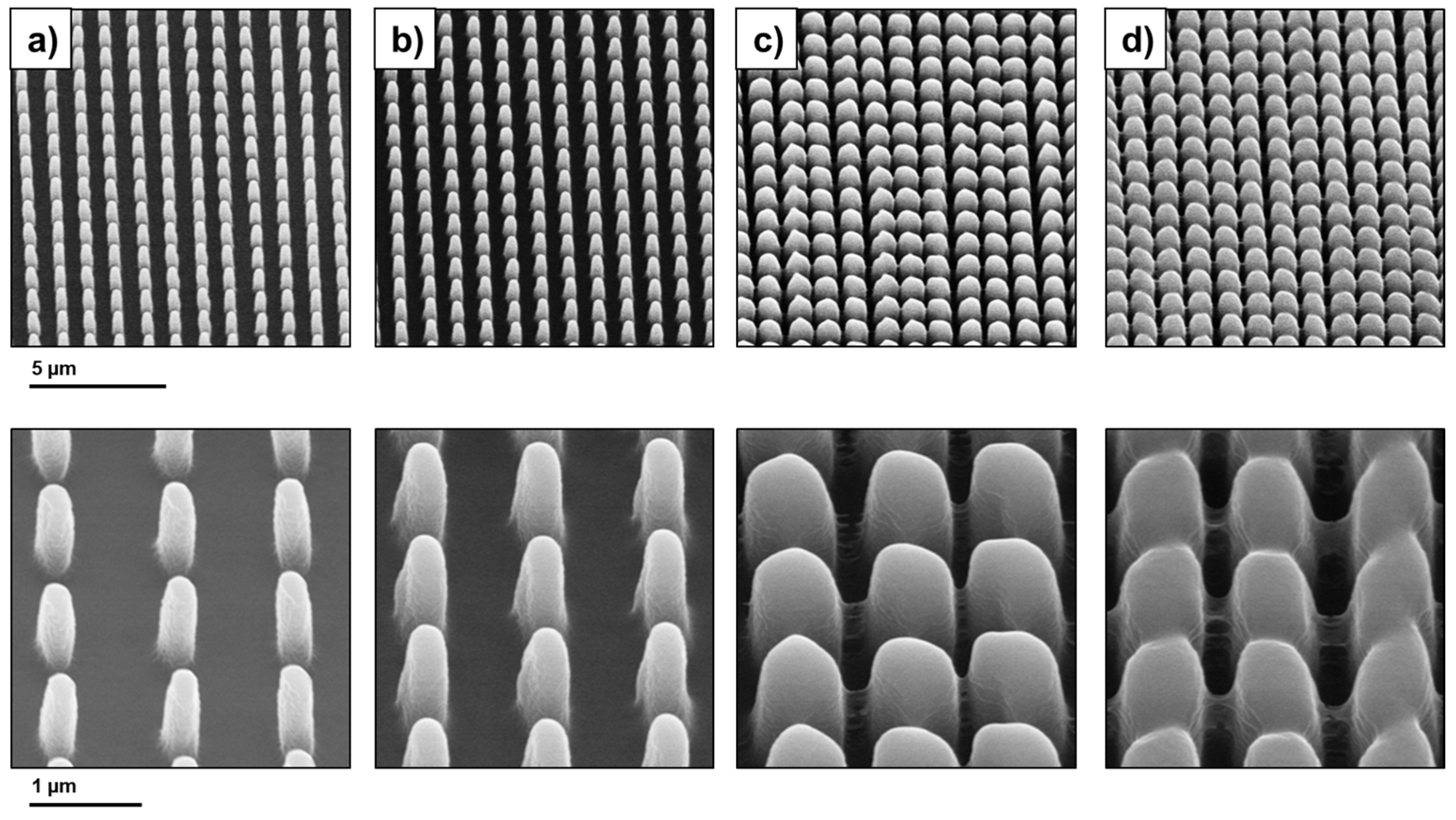
We fabricated and confirmed the four types of 3D-printed structures using optimized printing speed conditions (5000 mm/s) of 3D printing and analyzed them by SEM (Figure 3). According to the radii from 200 nm to 800 nm, magnified, tilted SEM images were also represented (Figure 3, bottom). Figure 3a shows the 3D nanostructure with a 200 nm diameter. As shown in the SEM images, the structures were uniformly fabricated without distortion. From left to right, Figure 3b–d shows the 3D nanostructure of 400, 600, and 800 nm, respectively. In the figures, we confirmed that the increase in nanostructure diameters decreases the distance between nanostructures. Moreover, regardless of the diameters, all the structures were uniformly fabricated. When the pillar radius was over 600 nm (Figure 3c,d), some bridges between pillars were also observed. Although the structures were not coated with Au or Ag for SERS application, we confirmed the uniformity of the 3D-printed nanostructures.

3.4. SERS Analysis of Au-Coated 3D Nanostructure

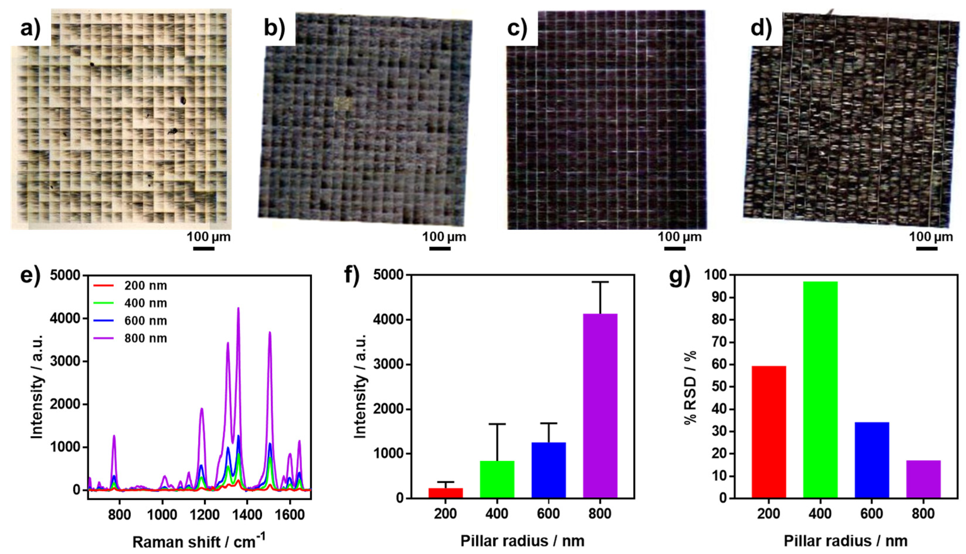
Through the optimization of printing speed, it was possible to fabricate a wide area of the 3D nanostructure according to the pillar radius (Figure 4). Before the controlling pillar radius, we gradually decreased the pillar radius (Figure S3). For investigation, 1 µM of CV was treated and analyzed. As a result, it was confirmed that the higher the pillar radius, the higher the SERS signal. However, the SERS intensity was very weak, and it was not easy to confirm the difference in change. Therefore, we controlled the pillar radius from 200 nm to 800 nm to show a clear change in SERS intensity (Figure 4a–d). Regardless of the pillar radius, all the 3D nanostructures were well-printed, without distortion or over-printed or not-printed areas. To the naked eye, the microscopic image colors darken with the increase in pillar radius from left to right. Because the nanostructures were printed using the algorithm used for spanning, the grid pattern was also observed. For SERS investigation, 100 µM of CV was dropped and dried on the 3D-printed nanostructures according to pillar radius. The SERS intensities were analyzed to calculate the average SERS intensities and uniformity according to the pillar radius.
Figure 4e shows the average SERS spectra of CV according to the pillar radius ranging from 200 nm to 800 nm. As a result, it was confirmed that the overall SERS spectrum intensity increased with the increase in pillar radius. For a detailed analysis, the intensities at 1360 cm−1, which is the characteristic peak of CV, were compared with the conditions (Figure 4f). Each value was 233.72 ± 138.76 (200 nm), 845.40 ± 821.70 (400 nm), 4256.299 ± 430.01 (600 nm), and 4140.84 ± 708.54 (800 nm), respectively. With high SERS efficiency, because it is crucial to obtain high uniformity, we analyzed the %RSD using SERS intensities (Figure 4g). In the result, the %RSD was the lowest at 17.11% in the 3D-printed nanostructures with an 800 nm pillar radius. These results are attributed to the numerous hotspots induced by the nano-gaps between the nano-pillars. Because the pillar radius is 800 nm, it is sufficient to make nano-gaps after Au/Cr coating. By controlling the pillar radius, the 3D-printed nanostructure with a 800 nm pillar radius at 5000 mm/s printing speed was optimized for SERS investigation, which has both high SERS efficiency and high uniformity.

3.5. SERS Analysis of Ag-Coated 3D Nanostructure

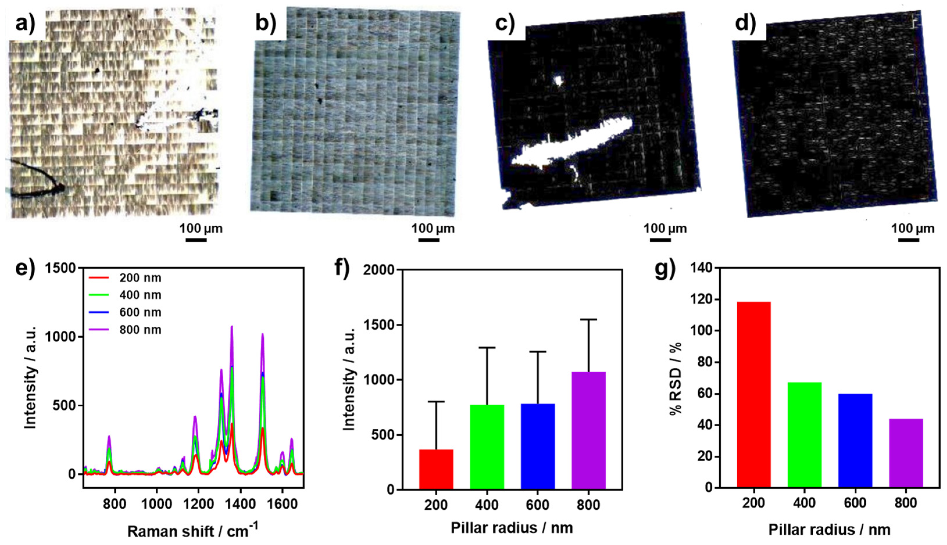
It is well-known that noble metals are suitable for SERS applications. Therefore, we performed a comparison test using Ag/Cr coating (Figure 5). The same method of investigation was used for the Au/Cr-coating 3D-printed nanostructures, where 100 µM of CV was treated on the substrates according to the pillar radius. In Figure 5a–d, the colors of the microscopic images were darkened with the increase in pillar radius from 200 nm to 800 nm. As for the Au/Cr-coating 3D-printed nanostructures, the overall SERS spectrum intensity was increased with the increase in pillar radius (Figure 5e). However, in comparison to the Au/Cr-coated 3D-printed nanostructures, the SERS intensities of 100 µM of CV were slightly lower in the case of the Ag/Cr coating. A more detailed analysis is represented in Figure 5f by calculating average SERS intensities at 1360 cm−1. Overall, SERS intensities have the same increment tendency as same as Au/Cr-coated nanostructures, but show bigger standard deviations than that of Au/Cr-coated nanostructures. In the %RSD calculations, the opposite tendency was confirmed with a comparison to the SERS intensity (Figure 5g). Consequently, the Ag/Cr-coated 3D nanostructure has the highest SERS efficiency when made using an 800 nm pillar radius at a 5000 mm/s printing speed.
These results mean that the highly uniform and efficient SERS substrate fabricated by the femtosecond laser 3D printer can be fabricated by the 800 nm pillar radius at the 5000 mm/s printing speed with both Au/Cr coating and Ag/Cr coating. The difference between the noble metals that are used (Au or Ag) may be induced by the coating conditions and oxidation of the metal. Due to the high SERS efficiency and uniformity, it is possible to use very reliable and sensitive SERS detection in various fields.

4. Conclusions

Femtosecond laser 3D printing has proven to be an effective method for fabricating high-uniformity, 3D-printed nanostructures with an enhanced surface-enhanced Raman scattering (SERS) efficiency. By optimizing printing conditions, specifically controlling the printing speed and pillar radius, the highest SERS intensity was achieved, with 800 nm radius pillars printed at a speed of 5000 mm/s. Compared to traditional substrate coatings such as gold or silver, the 3D-printed nanostructures demonstrated a superior reliability and efficiency in SERS substrate fabrication. These advancements have significant implications for various applications, including SERS substrates, biosensors, and medical devices. The precise control over pillar dimensions and the ability to tailor the nanostructures to specific requirements offer versatility and adaptability. Overall, femtosecond laser 3D-printed nanostructures present a remarkable breakthrough in the field, providing an exceptional performance and opening up new possibilities to enhance sensitivity and detection limits in analytical applications.

Supplementary Materials

The following supporting information can be downloaded at: https://www.mdpi.com/article/10.3390/chemosensors11060340/s1, Figure S1: 3D design of a single spot of 3D-printed SERS nanostructure with 25 × 25 µm2 size and 625 circular pillars in the area; Figure S2: Magnified average SERS spectra of 3D printed SERS nanostructures that printed as 10,000 mm/s; Figure S3: Gradient 3D-printed SERS nanostructure fabrication via a femtosecond laser printer. (a) Microscopic and SERS mapping images of gradient-printed nanostructure. (b) SERS spectra of 1 µM of CV-treated nanostructures. Changing colors from red to purple show the gradual decrease in pillar radius.

Author Contributions

Conceptualization, D.B.; investigation, W.K. (Woong Kim) and W.K. (Wooching Kim); writing—original draft preparation, W.K. (Woong Kim) and W.K. (Woochang Kim); writing—review and editing, D.B., J.P. and W.L.; supervision, D.B., J.P. and W.L.; funding acquisition, J.P. and W.L. All authors have read and agreed to the published version of the manuscript.

Funding

This study was supported by the National Research Foundation of South Korea (NRF) under Grant No. NRF-2022R1A2C4001990 and No. NRF-2023R1A2C2004964. In addition, this research was supported by “Regional Innovation Strategy (RIS)” through the National Research Foundation of Korea (NRF) funded by the Ministry of Education (MOE) (2021RIS-001(1345356234)) and the Korea Environment Industry & Technology Institute (KEITI) through its Ecological Imitation-based Environmental Pollution Management Technology Development Project funded by the Korea Ministry of Environment (MOE) (2019002800009).

Institutional Review Board Statement

Not applicable.

Informed Consent Statement

Not applicable.

Data Availability Statement

Data available on request due to restrictions e.g. privacy or ethical. The data presented in this study are available on request from the corresponding author. The data are not publicly available due to prepare a patent application.

Conflicts of Interest

The authors declare no conflict of interest.

References

  1. Kim, W.; Park, J.; Kim, W.; Jo, S.; Kim, M.; Kim, C.; Park, H.; Bang, D.; Lee, W.; Park, J. Bio-Inspired Ag Nanovilli-Based Sandwich-Type SERS Aptasensor for Ultrasensitive and Selective Detection of 25-Hydroxy Vitamin D3. Biosens. Bioelectron. 2021, 188, 113341. [Google Scholar] [CrossRef] [PubMed]
  2. Kim, W.; Lee, W.; Park, H.; Park, J.; Kim, W.; Kang, B.; Choi, E.; Kim, C.-S.; Park, J.-O.; Lee, G.; et al. Biomimetic Nano-Pine-Pollen Structure-Based Surface-Enhanced Raman Spectroscopy Sensing Platform for the Hypersensitive Detection of Toxicants: Cadmium and Amyloid. ACS Sustain. Chem. Eng. 2022, 10, 3180–3190. [Google Scholar] [CrossRef]
  3. Yuen, C.; Zheng, W.; Huang, Z. Principles of Surface-Enhanced Raman Spectroscopy: And Related Plasmonic Effects. J. Innov. Opt. Health Sci. 2008, 1, 267–284. [Google Scholar] [CrossRef]
  4. Kneipp, K.; Wang, Y.; Kneipp, H.; Perelman, L.T.; Itzkan, I.; Dasari, R.R.; Feld, M.S. Single Molecule Detection Using Surface-Enhanced Raman Scattering (SERS). Phys. Rev. Lett. 1997, 78, 1667–1670. [Google Scholar] [CrossRef] [Green Version]
  5. Futamata, M.; Maruyama, Y.; Ishikawa, M. Local Electric Field and Scattering Cross Section of Ag Nanoparticles under Surface Plasmon Resonance by Finite Difference Time Domain Method. J. Phys. Chem. B 2003, 107, 7607–7617. [Google Scholar] [CrossRef]
  6. Amendola, V.; Pilot, R.; Frasconi, M.; Maragò, O.M.; Iatì, M.A. Surface Plasmon Resonance in Gold Nanoparticles: A Review. J. Phys. Condens. Matter 2017, 29, 203002. [Google Scholar] [CrossRef]
  7. Jain, P.K.; Huang, X.; El-Sayed, I.H.; El-Sayed, M.A. Review of Some Interesting Surface Plasmon Resonance-Enhanced Properties of Noble Metal Nanoparticles and Their Applications to Biosystems. Plasmonics 2007, 2, 107–118. [Google Scholar] [CrossRef]
  8. Moreno, V.; Zougagh, M.; Ríos, Á. Analytical Nanometrological Approach for Screening and Confirmation of Titanium Dioxide Nano/Micro-Particles in Sugary Samples Based on Raman Spectroscopy—Capillary Electrophoresis. Anal. Chim. Acta 2019, 1050, 169–175. [Google Scholar] [CrossRef]
  9. Pal, P.; Bonyár, A.; Veres, M.; Himics, L.; Balázs, L.; Juhász, L.; Csarnovics, I. A Generalized Exponential Relationship between the Surface-Enhanced Raman Scattering (SERS) Efficiency of Gold/Silver Nanoisland Arrangements and Their Non-Dimensional Interparticle Distance/Particle Diameter Ratio. Sens. Actuators A Phys. 2020, 314, 112225. [Google Scholar] [CrossRef]
  10. Tian, Z.Q. Surface-Enhanced Raman Spectroscopy: Advancements and Applications. J. Raman Spectrosc. 2005, 36, 466–470. [Google Scholar] [CrossRef]
  11. Campion, A.; Kambhampati, P. Surface-Enhanced Raman Scattering. Chem. Soc. Rev. 1998, 27, 241–250. [Google Scholar] [CrossRef]
  12. Li, D.W.; Zhai, W.L.; Li, Y.T.; Long, Y.T. Recent Progress in Surface Enhanced Raman Spectroscopy for the Detection of Environmental Pollutants. Microchim. Acta 2014, 181, 23–43. [Google Scholar] [CrossRef]
  13. Sun, J.; Gong, L.; Wang, W.; Gong, Z.; Wang, D.; Fan, M. Surface-enhanced Raman Spectroscopy for On-site Analysis: A Review of Recent Developments. Luminescence 2020, 35, 808–820. [Google Scholar] [CrossRef]
  14. Fritzler, K.B.; Prinz, V.Y. 3D Printing Methods for Micro- and Nanostructures. Physics-Uspekhi 2019, 62, 54–69. [Google Scholar] [CrossRef]
  15. Jaitpal, S.; Chavva, S.R.; Mabbott, S. 3D Printed SERS-Active Thin-Film Substrates Used to Quantify Levels of the Genotoxic Isothiazolinone. ACS Omega 2022, 7, 2850–2860. [Google Scholar] [CrossRef] [PubMed]
  16. Mu, J.; Li, J.; Li, W.; Luo, Q.; Gu, C. Hollow Metallic Pyramid Plasmonic Structures Fabricated by Direct Laser Writing and Electron Beam Evaporation. Microelectron. Eng. 2013, 110, 307–310. [Google Scholar] [CrossRef]
  17. Braun, A.; Maier, S.A. Versatile Direct Laser Writing Lithography Technique for Surface Enhanced Infrared Spectroscopy Sensors. ACS Sens. 2016, 1, 1155–1162. [Google Scholar] [CrossRef]
  18. Yoshikawa, H.; Hironou, A.; Shen, Z.; Tamiya, E. Versatile Micropatterning of Plasmonic Nanostructures by Visible Light Induced Electroless Silver Plating on Gold Nanoseeds. ACS Appl. Mater. Interfaces 2016, 8, 23932–23940. [Google Scholar] [CrossRef]
  19. Bai, S.; Serien, D.; Hu, A.; Sugioka, K. 3D Microfluidic Surface-Enhanced Raman Spectroscopy (SERS) Chips Fabricated by All-Femtosecond-Laser-Processing for Real-Time Sensing of Toxic Substances. Adv. Funct. Mater. 2018, 28, 1706262. [Google Scholar] [CrossRef]
  20. Li, X.; Yuan, G.; Yu, W.; Xing, J.; Zou, Y.; Zhao, C.; Kong, W.; Yu, Z.; Guo, C. A Self-Driven Microfluidic Surface-Enhanced Raman Scattering Device for Hg2+ Detection Fabricated by Femtosecond Laser. Lab Chip 2020, 20, 414–423. [Google Scholar] [CrossRef]
  21. Sugioka, K. Hybrid Femtosecond Laser Three-Dimensional Micro-and Nanoprocessing: A Review. Int. J. Extrem. Manuf. 2019, 1, 012003. [Google Scholar] [CrossRef]
  22. Sugioka, K.; Cheng, Y. Femtosecond Laser Three-Dimensional Micro-and Nanofabrication. Appl. Phys. Rev. 2014, 1, 041303. [Google Scholar] [CrossRef] [Green Version]
  23. Sima, F.; Sugioka, K.; Vázquez, R.M.; Osellame, R.; Kelemen, L.; Ormos, P. Three-Dimensional Femtosecond Laser Processing for Lab-on-a-Chip Applications. Nanophotonics 2018, 7, 613–634. [Google Scholar] [CrossRef]
  24. Bai, S.; Sugioka, K. Recent Advances in the Fabrication of Highly Sensitive Surface-Enhanced Raman Scattering Substrates: Nanomolar to Attomolar Level Sensing. Light Adv. Manuf. 2021, 2, 186. [Google Scholar] [CrossRef]
  25. Bharati, M.S.S.; Byram, C.; Soma, V.R. Femtosecond Laser Fabricated Ag@Au and Cu@Au Alloy Nanoparticles for Surface Enhanced Raman Spectroscopy Based Trace Explosives Detection. Front. Phys. 2018, 6, 28. [Google Scholar] [CrossRef] [Green Version]
  26. Long, L.; Ju, W.; Yang, H.Y.; Li, Z. Dimensional Design for Surface-Enhanced Raman Spectroscopy. ACS Mater. Au 2022, 2, 552–575. [Google Scholar] [CrossRef]
  27. Huang, C.Y.; Tsai, M.S. Tunable Silver Nanoparticle Arrays by Hot Embossing and Sputter Deposition for Surface-Enhanced Raman Scattering. Appl. Sci. 2019, 9, 1636. [Google Scholar] [CrossRef] [Green Version]
  28. Todeschini, M.; Bastos Da, A.; Fanta, S.; Jensen, F.; Wagner, J.B.; Han, A. Influence of Ti and Cr Adhesion Layers on Ultrathin Au Films. ACS Appl. Mater. Interfaces 2017, 9, 35. [Google Scholar] [CrossRef] [Green Version]
  29. Kim, W.; Lee, W.; Choi, H.; Lee, G.; Son, J.; Lee, S.W.; Park, J.; Kim, W.; Kim, M.; Yoon, D.S.; et al. Bioinspired Micro Glue Threads Fabricated by Liquid Bridge-to-Solidification as an Effective Sensing Platform. ACS Sens. 2020, 5, 1977–1986. [Google Scholar] [CrossRef]
Figure 1. 3D-printed SERS nanostructure fabrication via a femtosecond laser printer. (a) Schematic illustrations of SERS nanostructure fabrication according to pillar radius. The pillar radius was controlled from 200 nm to 800 nm. After printing, chrome, and gold or silver films were coated on the printed nanostructures. (b) Photo image of printed SERS nanostructure with a 0.5 × 0.5 mm2 area. The yellow dotted box shows a magnified image. (c,d) microscopic images of 3D-printed SERS nanostructure.
Chemosensors 11 00340 g001
Figure 2. Optimization of 3D-printed SERS nanostructure depending on the printing speed and the pillar radius. (a) Microscopic images of 3D-printed SERS nanostructures printed as 1000 mm/s. From left to right, the pillar radius of 3D-printed SERS nanostructures was 200, 400, and 800 nm, respectively. (b) Average SERS spectra of each SERS mapping image using 1 µM of CV as Raman indicator. (c,d) Microscopic images and average SERS spectra of 3D-printed SERS nanostructures that printed as 5000 mm/s, respectively. (e,f) Microscopic images and average SERS spectra of 3D-printed SERS nanostructures that printed as 10,000 mm/s, respectively. All the analyses were conducted in the same manner. (g) SERS intensities at 1360 cm−1 of CV according to the printing speed and the pillar radius. (h) Uniformity analysis using SERS mapping images according to the printing speed and the pillar radius.
Chemosensors 11 00340 g002
Figure 3. Tilted SEM images of 3D-printed nanostructure depending on the pillar radius. From left to right, the pillar radius was controlled as (a) 200 nm, (b) 400 nm, (c) 600 nm, and (d) 800 nm, respectively. The bottom SEM images are magnified images of these, respectively.
Chemosensors 11 00340 g003
Figure 4. Optimization of Au-coated 3D-printed SERS nanostructures according to the pillar radius. (ad) Microscopic images of 3D-printed SERS nanostructures with 200, 400, 600, and 800 nm, respectively. (e) Average SERS spectra of CV on the different 3D-printed SERS nanostructures. (f) SERS intensities at 1360 cm−1 according to the pillar radius ranging from 200 to 800 nm. (g) Uniformity analysis using SERS mapping images according to the pillar radius.
Chemosensors 11 00340 g004
Figure 5. Optimization of Ag-coated 3D-printed SERS nanostructures according to the pillar radius. (ad) Microscopic images of 3D-printed SERS nanostructures with 200, 400, 600, and 800 nm, respectively. (e) Average SERS spectra of CV on the different 3D-printed SERS nanostructures. (f) SERS intensities at 1360 cm−1 according to the pillar radius ranging from 200 to 800 nm. (g) Uniformity analysis using SERS mapping images according to the pillar radius.
Chemosensors 11 00340 g005
Disclaimer/Publisher’s Note: The statements, opinions and data contained in all publications are solely those of the individual author(s) and contributor(s) and not of MDPI and/or the editor(s). MDPI and/or the editor(s) disclaim responsibility for any injury to people or property resulting from any ideas, methods, instructions or products referred to in the content.