Article

Pd-Nanoparticle-Decorated Multilayered MoS2 Sheets for Highly Sensitive Hydrogen Sensing

by
Shuja Bashir Malik
1,2,
Fatima Ezahra Annanouch
1,2,* and
Eduard Llobet
1,2
1
Departament d’Enginyeria Electronica, Universitat Rovira i Virgili, MINOS, Països Catalans 26, 43007 Tarragona, Spain
2
Institut Universitari de Recerca en Sostenibilitat, Canvi Climàtic i Transició Energètica, Universitat Rovira i Virgili, Joanot Martorell 15, 43480 Vila-seca, Spain
*
Author to whom correspondence should be addressed.
Chemosensors 2023, 11(11), 550; https://doi.org/10.3390/chemosensors11110550
Submission received: 6 September 2023 / Revised: 20 October 2023 / Accepted: 24 October 2023 / Published: 26 October 2023

Abstract

:
In this work, efficient hydrogen gas sensors based on multilayered p-type bare MoS2 and Pd-decorated MoS2 were fabricated. MoS2 was deposited onto alumina transducers using an airbrushing technique to be used as a sensing material. Aerosol-assisted chemical vapor deposition (AACVD) was used to decorate layered MoS2 with Pd nanoparticles at 250 °C. The bare and Pd-decorated MoS2 was characterized using field emission scanning electron microscopy (FESEM), high-resolution transmission electron microscopy (HR-TEM), X-ray diffraction (XRD), and Raman spectroscopy. The characterization results reveal the multilayered crystalline structure of MoS2 with successful Pd decoration. The size of the Pd nanoparticles ranges from 15 nm to 23 nm. Gas sensing studies reveal that a maximum response of 55% is achieved for Pd-decorated MoS2 operated at 150 °C to 100 ppm of H2, which is clearly below the explosive limit (4%) in air. The higher sensitivity due to Pd nanoparticle decoration was owed to a spillover effect. This study reveals that the sensitivity of the sensors is highly dependent on the amount of Pd decoration. Moreover, sensor responses increase slightly when exposed to 50% relative humidity (RH at 25 °C).

1. Introduction

The ever-increasing demand for sustainable and clean energy sources has put hydrogen (H2) at the forefront as one of the most promising candidates for the next generation of energy. Due to the abundance of hydrogen in nature, it offers the potential in the future to replace fossil fuels as its combustion yields water; thus, it will [1] significantly reduce greenhouse gas emissions [2]. However, hydrogen is highly explosive and flammable (air mixtures at H2 concentrations above 4%), which demands the utmost caution in its storage and handling [3]. Even a small leakage of hydrogen can pose a grave threat to safety. Therefore, the development of highly sensitive and selective hydrogen gas sensors with fast detection and recovery are of paramount importance to detect and mitigate potential hazards associated with hydrogen storage, transport, and leakage.
Metal oxide gas sensors (MOX) have been widely used for hydrogen sensing [4], but they suffer from several limitations like poor selectivity and a high working temperature (200–400 °C) [5,6,7]. This leads to an increase in the power consumption and, at the same time, reduces a sensor’s lifetime by inducing changes in the material morphology [8]. Moreover, with hydrogen being extremely flammable, sensors working at high temperatures could be potentially dangerous [9], requiring necessary remedies to mitigate damage. Recently, the scientific community has turned its attention towards two-dimensional materials (2D) to overcome the shortcomings of MOX sensors. Indeed, 2D materials have garnered tremendous attention due to their unique electronic and remarkable sensing properties [10,11]. Among 2D materials, on the one hand, graphene has demonstrated outstanding sensing capabilities for toxic gases like NO2, ammonia, and CO [12,13]. Decorating graphene with metal nanoparticles (NP) like Au, Pt, Pd, or Ag has been found to enhance the sensitivity to gas molecules due to the catalytic effect of the nanoparticles [14,15].
On the other hand, transition metal dichalcogenides (TMDs) have emerged as an exciting class of 2D materials for gas sensing applications [16,17,18,19]. Among the TMDs, molybdenum disulfide (MoS2) has garnered significant interest and attention due to its exceptional sensing, electronic, optical, and catalytic properties [3,20,21]. MoS2 is a layered structure, with each layer consisting of covalently bonded Mo-S atoms, and neighboring layers are stacked to each other via van der Waals forces [22]. Bulk MoS2 has an indirect band gap of 1.2 eV, while, as for the atomically thin MoS2 sheets, there is a transition to a direct bandgap of 1.8 eV, leading to enhanced charge transport, high specific surface areas due to their sheet-like structures with large basal planes and highly reactive edges, and increased electron concentration at the surface [23]. These properties of MoS2 make it highly desirable for the development of next-generation memory devices [24], photodetectors [25], solar cells [26], and gas sensors [3,11,27].
Several research works have demonstrated the potential of MoS2-based gas sensors for detecting gases like nitrogen dioxide (NO2) [28], ammonia (NH3) [29], nitric oxide (NO) [30], and hydrogen [11,18,27]. Duesberg et al. demonstrated the synthesis of MoS2 patterns and recorded high-sensitivity detection of ammonia with a limit of detection at the ppm level [31]. Zhou et al. reported Schottky-contact MoS2-based sensors which are sensitive to 20 ppb and 1 ppm of NO2 and NH3, respectively [32]. Zhang and co-workers presented the influence of the thickness on the performance of MoS2 gas sensors to NO [33]. Zhou et al. demonstrated a MoS2-based sensor with a 92.6% response to 500 ppm of CO at 230 °C [34]. Moreover, Agarwal et al. presented a highly sensitive and fast hydrogen sensor based on monolayer MoS2 pyramid structures with a 69.1% response to 1% of hydrogen [3].
However, sensors based on bare MoS2 suffer from sluggish response–recovery speeds and low sensitivity, especially when it comes to the detection of hydrogen gas [3,35]. We have seen that functionalizing the host matrix with a determined noble metal enhances the sensitivity and the selectivity of the sensor to a specific gas. Based on our previous works, we found that CuO nanoparticles are very suitable for the detection of H2S [36]. Additionally, we showed that Pd/PdO nanoparticles have highly enhanced the sensitivity and selectivity of WO3 to H2 [37]. Additionally, it was reported that the incorporation of noble metal nanoparticles onto MoS2 has shown promise in detecting hydrogen with low power consumption and high sensitivity [9,27,35,38,39,40]. The improved sensing response attributed to the incorporation of noble metals is a result of electronic sensitization (ES) and chemical sensitization (CS) [41,42]. Electronic sensitization involves the oxidized form of the noble metal creating electron-depletion layers (EDLs) at the interface between the noble metal and the sensing layer [41,43], while chemical sensitization arises from a catalytic surface reaction in which noble metals offer low energy sites for the gas adsorption, leading to enhanced sensor sensitivity via a spillover process [41,44]. Noble metal decoration not only enhances sensitivity and helps in decreasing the optimal sensing temperature but helps in enhancing the long-term stability of the sensors as well [41]. Irrespective of the functionalization process employed, two crucial factors governing noble metal decoration are the amount and the size of the nanoparticles. The optimization of nanoparticle decoration amounts on the sensing layer is important as it directly influences the dissociation of gas molecules. If the decoration is insufficient, the sensitization effect will be diminished. Conversely, excessive decoration would lead to the formation of a continuous film, leading to reduced sensitivity [45].
MoS2 offers functional groups on both the basal plane and edge sites, which allows for easy incorporation of adatoms on the surface [33,46,47]. The most common method to deposit nanosized metal nanoparticles on MoS2 using a vacuum is with an e-beam evaporator, as explored by Park et al. to decorate MoS2 with Pt nanoparticles for NH3 and H2S detection [48]. Suh et al. also utilized an e-beam evaporator to decorate Pd and Au on MoS2 to demonstrate the selectivity of the composite to C2H5OH, H2, NH3, and NO2 [49]. Nonetheless, vacuum-based processes pose drawbacks such as high costs and power consumption, limiting gas sensor development. Burman et al. employed a solution process using glucose as a reducing agent for Au doping on MoS2 for detecting ammonia with high sensitivity [50]. Huang et al. took advantage of various capping and reducing agents for the epitaxial growth of Pd, Pt, and Ag metal nanostructures on MoS2 [51]. The use of reducing agents for nanostructure decorations indeed facilitates the reduction of metal precursors into controllable shapes of metal nanoparticles but may act as a barrier for gas sensing [52]. Kim et al. addressed this issue by using a solution process reaction without reducing agents to decorate 2D MoS2 nanoflakes with Au, Pt, and Pd for selective ammonia, hydrogen, and ethanol sensing [52]. Lee and co-workers deposited Pt using atomic layer deposition (ALD) on MoS2 for H2 sensing [53].
Herein, we report the development of bare and Pd-NP-decorated multilayer MoS2 for hydrogen sensing. Our method is a simple two-step procedure: (i) airbrushing MoS2 onto alumina substrates, followed by (ii) low-temperature AACVD decoration of Pd nanoparticles onto MoS2 sensing layers. To the best of our knowledge, none of the reported works have combined airbrushing and low-temperature AACVD methods to functionalize TMD materials. The sensing materials were characterized with FESEM, HRTEM, XRD, and Raman spectroscopy to study the morphology, crystal structure, and decoration characteristics. We investigated the chemiresistive sensing mechanism of bare and Pd-decorated MoS2 and studied the impact of Pd decoration on the sensing properties of MoS2 to hydrogen gas. The sensors display a response of 55% to 100 ppm of hydrogen gas at 150 °C and show a clear impact of Pd decoration on hydrogen sensitivity.

2. Experimental Section

2.1. Materials, Chemicals, and Sensor Fabrication

2.1.1. Materials and Sensor Fabrication

MoS2 powder (CAS:1317-33-5) was purchased from Sigma-Aldrich, Madrid, Spain and used without further modifications. A total of 20 mg of MoS2 powders was sonicated in 10 mL of ethanol (Scharlab, Barcelona, Spain CAS: 64-17-5) for 45 min to obtain a homogenous suspension. The suspension was immediately airbrushed onto alumina transducers (Ceram Tech GmBH, Plochingen, Germany) to achieve MoS2 thin films coating the interdigitated electrode area. Nitrogen was used as a carrier gas during the airbrushing. In order to achieve thin films of reproducible thickness, the resistance of the films was monitored during deposition by connecting the alumina transducer to a multimeter. As soon as the desired resistance of the material was reached, the deposition process was stopped. Samples were fabricated in four sets for each type of material. The average resistance of a pristine set of sensors was 400 MΩ ± 12 MΩ, while, as for sensors with 1 mg of Pd precursor (MoS2-Pd_1), the average resistance was 72 MΩ ± 4 MΩ. Also, for the sample with 2 mg of Pd precursor (MoS2-Pd_2), the average resistance was 55 MΩ ± 6 MΩ. All these resistance values were calculated at room temperature. Moreover, the average thickness of the deposited layers was calculated to be around 582 nm using focus ion beam (FIB). The FESEM images of the thickness analysis of the sensing layer are presented in Figure S1.

2.1.2. Pd-Nanoparticle-Decorated MoS2 Nanosheets Using AACVD Method

Palladium nanoparticles were incorporated onto the fabricated MoS2 sensors using aerosol-assisted chemical vapor deposition (AACVD). The reaction was performed at comparatively low temperature of 250 °C. To study the effect of Pd concentration on the sensor responses, two amounts of the palladium precursor were used to decorate MoS2 sensors. In a typical synthesis procedure, 1 mg and 2 mg of Palladium (II) acetylacetonate (Sigma-Aldrich, Madrid, Spain CAS: 14024-61-4) were dissolved in 5 mL methanol (CAS: 67-56-1). The solution was ultrasonicated to ensure full solubilization. The solution was placed in an ultrasonic humidifier to generate aerosol. N2 gas with a flow of 0.5 L/min was used as a carrier gas to transport the aerosol to the MoS2 sensors preheated at 250 °C in a hot wall reactor. The AACVD method is similar to our previous reported works [54,55]. The deposition time was about 5 min; after that, the chamber was left to cool down naturally. The sensors were named according to the Pd decoration concentration, viz., MoS2-Pd_1 and MoS2-Pd_2 for 1 mg and 2 mg precursor amounts, respectively.

2.2. Material Characterization Techniques

The morphology of the prepared samples was analyzed using a field emission scanning electron microscope (FESEM-Thermo Scientific Scios 2, Waltham, MA, USA). The FESEM microscope used in this study is equipped with EDX as well to calculate the wt. % of palladium nanoparticles. Moreover, the FESEM equipment is also equipped with the focus ion beam (FIB) tool used here to calculate the thickness of the sensing layer. The crystal structure was analyzed via X-ray diffraction using a Bruker AXS D8 diffractometer equipped with parallel incident beam (Gobel mirror) vertical θ-θ goniometer, XYZ motorized stage, and with a GADDS (General Area Diffraction System). A JEOL F200 TEM ColdFEG (JEOL, Tokyo, Japan) operated at 200 kV was used for the high-resolution transmission electron microscopy (HRTEM) characterization. EDX spectra and elemental analysis was performed using the same HRTEM equipment. The Raman spectra were recorded using a Renishaw in Via, laser 514 nm, ion argon-Novatech, 25 mW.

2.3. Gas Sensing Measurements

The gas sensing measurements were conducted using a homemade detection system in a Teflon® chamber with a volume of 35 mL. The chamber is designed to accommodate four sensors simultaneously. The chamber consists of an inlet connected to the gas delivery system and an outlet which is connected to the exhaust. Commercial alumina substrates with interdigitated platinum electrodes (300 µm electrode gap) on the front side and a platinum resistive meander on the back side were used to deposit the sensing material. The sensor responses were recorded by monitoring the sensing material resistance using an Agilent-34972A data acquisition system. Calibrated cylinders of NO2 (total concentration, 1 ppm), H2 (total concentration, 1000 ppm), NH3 (total concentration, 100 ppm), CO (total concentration, 100 ppm), and benzene (total concentration, 10 ppm) were mixed with pure synthetic air using Bronkhorst mass-flow controllers. A constant flow rate of 100 mL min−1 was maintained during all the experiments. The sensors were exposed to the analyte gas for 10 min and subsequently cleaned in dry air for 60 min. The cleaning time to recover the baseline was adapted according to the sensor operating temperature; 60 min for 50 °C, 100 °C, and 150 °C and 120 min for room temperature operation. Prior to gas sensing measurements, sensors were kept under a constant flow of dry air for a minimum of 5 h to completely stabilize their initial baseline resistance. The sensor responses were calculated using Equation (1) for reducing gas species and Equation (2) for oxidizing gas species.
( R g a s R a i r R a i r × 100 )   %
( R a i r R g a s R a i r × 100 )   %
where  R a i r  and  R g a s  are the real-time resistances of the sensor exposed to air and to analyte, respectively.

3. Results and Discussions

3.1. Material Characterization

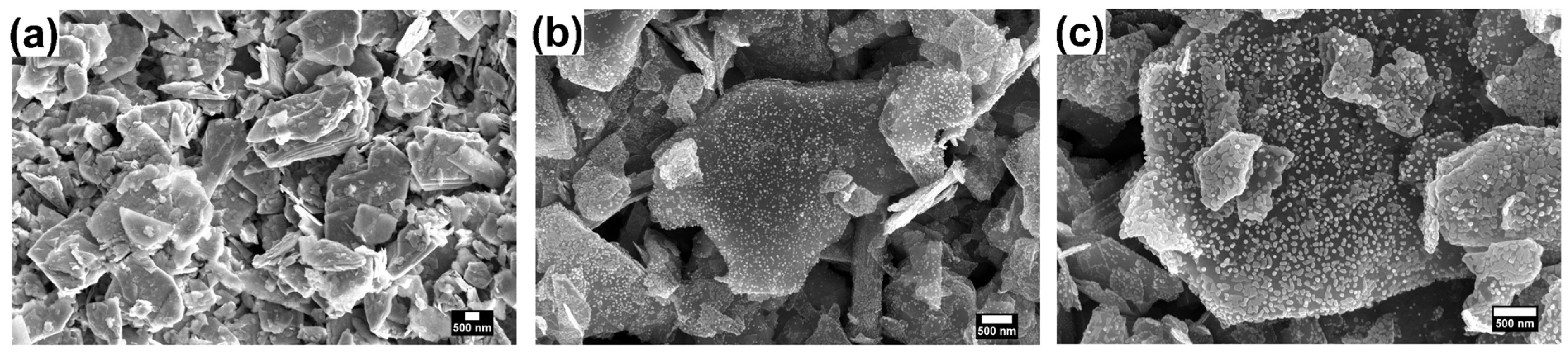
3.1.1. FESEM Analysis

Figure 1 depicts the FESEM images of the sensing materials. Upon analysis, it is evident that the deposited MoS2 exhibits a multilayered structure, as shown in Figure 1a. The size of the MoS2 structures varies from 200 nm to 1.5 µm (edge to edge), displaying clear and distinct ridges. In the case of MoS2-Pd_1, most of the decorated Pd nanoparticles are spherical with an average size of 15 nm, as shown in Figure 1b. In the case of MoS2-Pd_2, the decorated nanoparticles are a mix of spherical and rice-grain shaped with an average size slightly larger (23 nm) than that observed in MoS2-Pd_1, as illustrated in Figure 1c. Decorating with a higher concentration of palladium leads to higher coverage, which can be seen in the FESEM images. Different Pd decoration amounts were used to check the impact of the decoration amount on the gas sensing properties of the material. The decoration of the sensors was kept at low concentrations to avoid hindering the transport of dissociated hydrogen atoms to the MoS2 channel. This could be owed to the hampering of the catalytic effect due to the increased concentration of Pd [53]. Moreover, it is clear that the deposition of metal nanoparticles has no visible influence on the morphology of the MoS2. Also, an Energy Dispersive X-ray Analysis (EDX) of the samples was conducted to determine the average weight percentage (wt. %) of Palladium (Pd) in the respective samples. The EDX analysis was carried out at various spots on the samples; the resulting data were analyzed to calculate the average wt. % of palladium. Based on the calculations, the average wt. % of Pd in the MoS2-Pd_1 sample was 7.27 wt. %, while, as in the MoS2-Pd_2 sample, the wt. % of palladium was 11.69 wt. %.

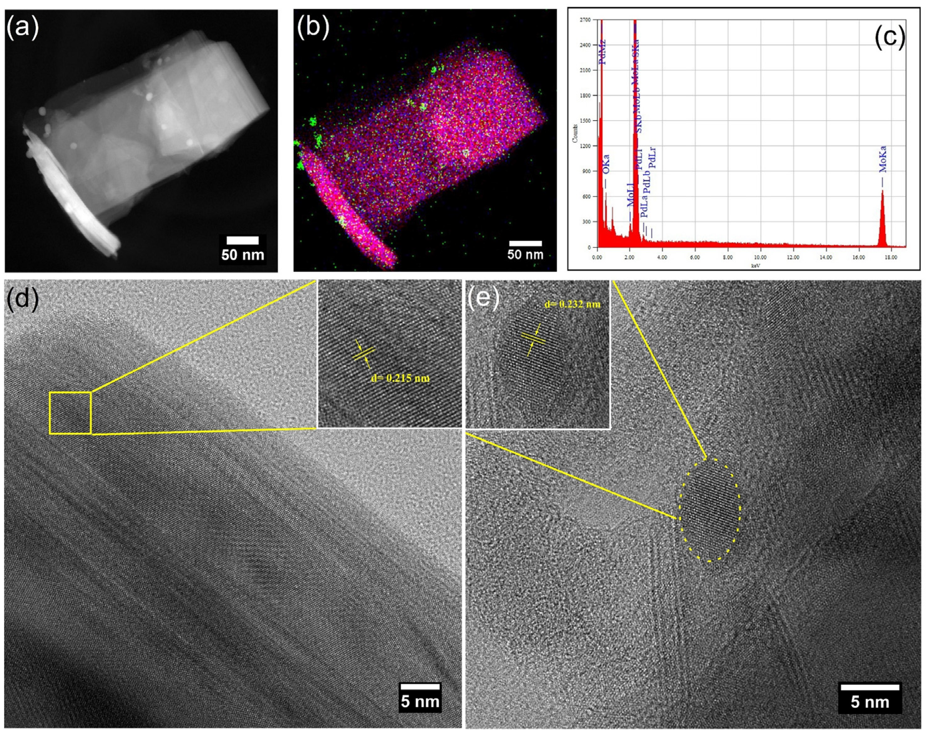
3.1.2. HRTEM Analysis
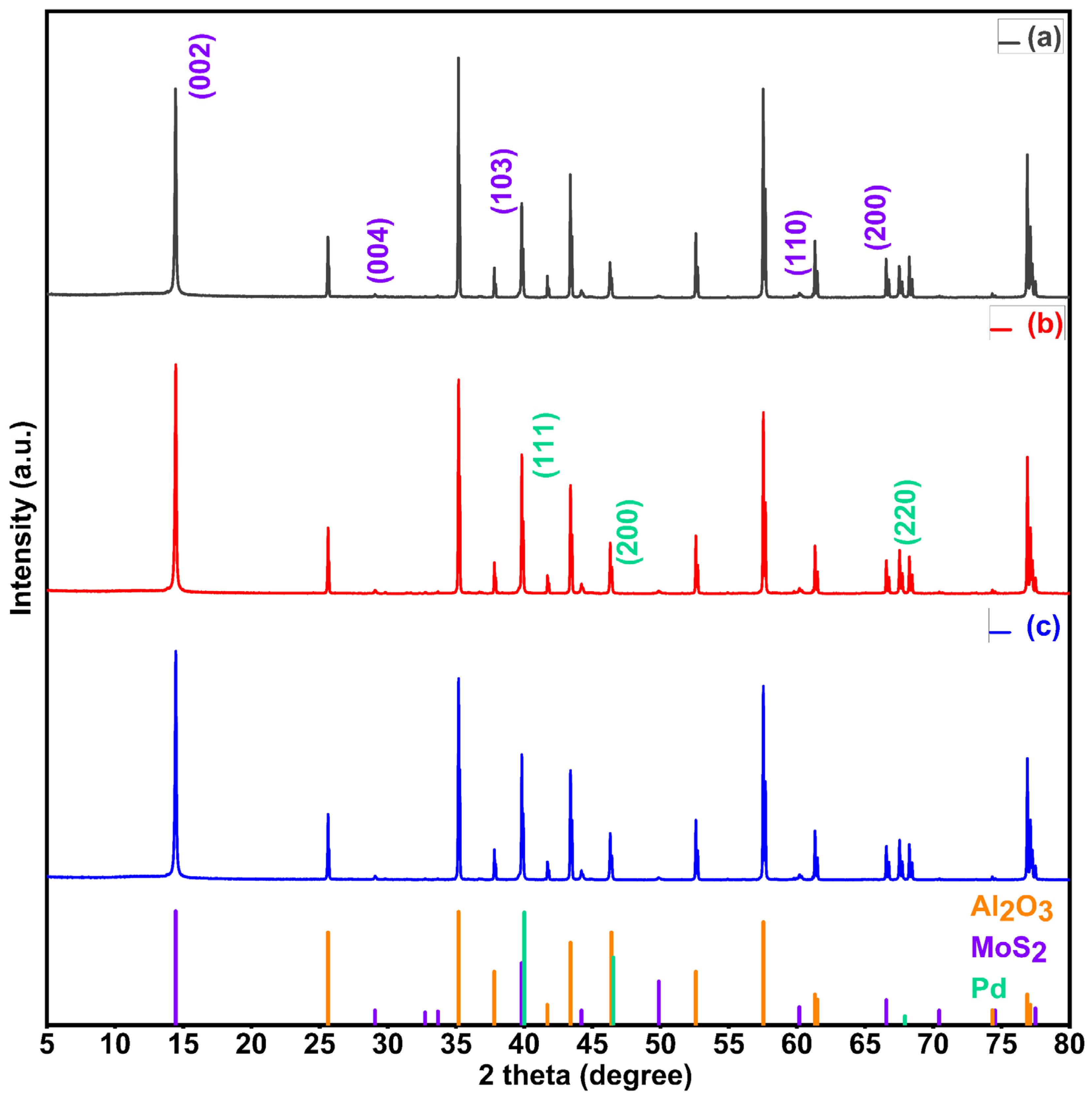
Supplementing the FESEM morphological data, an HRTEM analysis of one of the sensing materials, MoS2-Pd_2, was performed combined with EDX spectroscopy. Pd-decorated MoS2 films were scraped off the alumina substrate and drop-casted over carbon-coated copper grids. Analysis of the HRTEM results reveals the crystalline layered structure of the MoS2 with successful Pd decoration, as shown in Figure 2a,b. At some places, the layers are randomly oriented, while at other places the layers are stacked one on other. EDX spectra and HRTEM images of the sensing material are presented in Figure 2c–e, respectively. EDX analysis revealed the presence of Pd nanoparticles on MoS2 sheets. Upon further analysis, we verified the interlayer distance, with d equal to 0.215 nm corresponding to the (103) plane of MoS2 (ICDD card number: 65-1951) as shown in Figure 2d. The d-spacing calculated for Pd nanoparticles is 0.232 nm, which corresponds to the (111) plane of Pd (ICDD card number 88-2335). The interlayer distance results of both MoS2 and palladium were confirmed with XRD analysis.

3.1.3. XRD

The crystal structure of the sensing films was analyzed using an X-ray diffraction (XRD) method. Figure 3 shows the XRD diffractogram recorded from pristine MoS2 and Pd-decorated MoS2 in the range of 2θ = 5° to 80°. The observed diffraction peaks match with the hexagonal phase of MoS2 (ICDD card number: 65-1951) with lattice constants a = 0.316 nm and c = 1.2294 nm belonging to the P63/mmc space group. The major diffraction peaks can be indexed to the (002) at 14.42°, (102) at 35.88°, (103) at 39.56°, and (105) at 49.81° lattice planes. Some additional peaks are observed in Figure 3b,c. These peaks can be indexed to palladium (ICDD card number: 88-2335). The diffraction peaks of palladium match the cubic phase with lattice constant a = 0.39 nm (Fm-3m space group). At 2θ = 40.01, 46.53, and 67.92, the peaks of MoS2 and Al2O3 almost coincide with the peaks of Pd. Hence, in Figure 3b,c, the peaks are more intense than those in Figure 3a, which corresponds to pristine MoS2. This confirms the presence of Pd decorating the surface of MoS2.

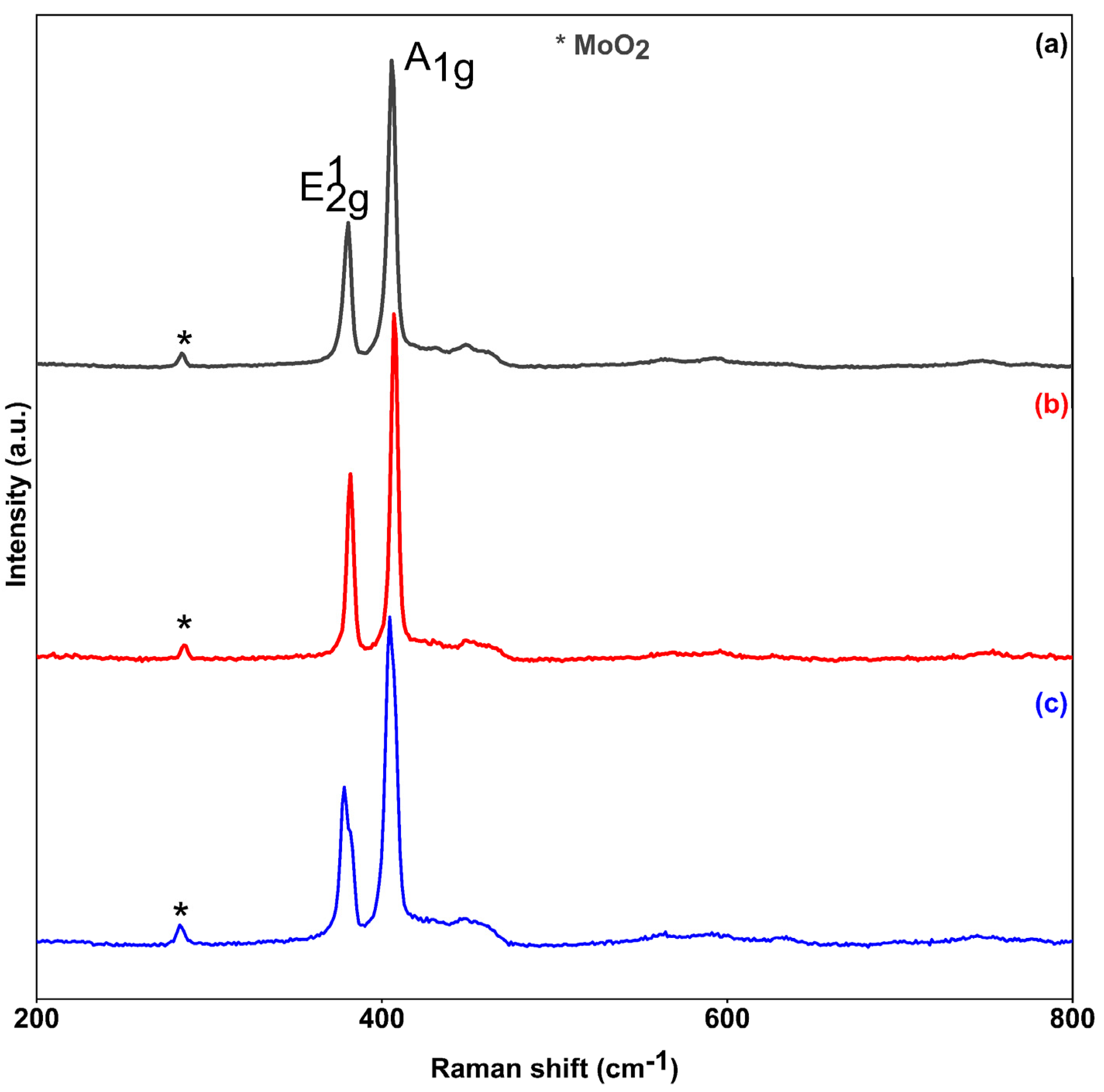
3.1.4. Raman Spectroscopy

Figure 4 shows the typical Raman spectra of pristine and Pd-decorated MoS2. The Raman spectra of all the samples show peaks near 400 cm−1, which confirms the 2H phase of MoS2. The two characteristic peaks signify the vibration modes for MoS2 E 2 g 1 , which corresponds to in-plane vibration of the molybdenum atom and is opposite to two sulfur atoms, and  A 1 g , mode which corresponds to the out-of-plane vibration of sulfur atoms (Mo atom being immobile) [56]. In addition to the main characteristic peaks, the small peak at ~283 cm−1 can be assigned to the MoO2 phase [57,58]. Table 1 summarizes the Raman peak positions of all the samples. The values of Δ provide the information about the number of layers in the MoS2. As can be seen from the table, Δ ≥ 25, indicating the multilayered structure of MoS2 [59,60]. This is in agreement with the FESEM and HRTEM results.

3.2. Gas Sensing Results

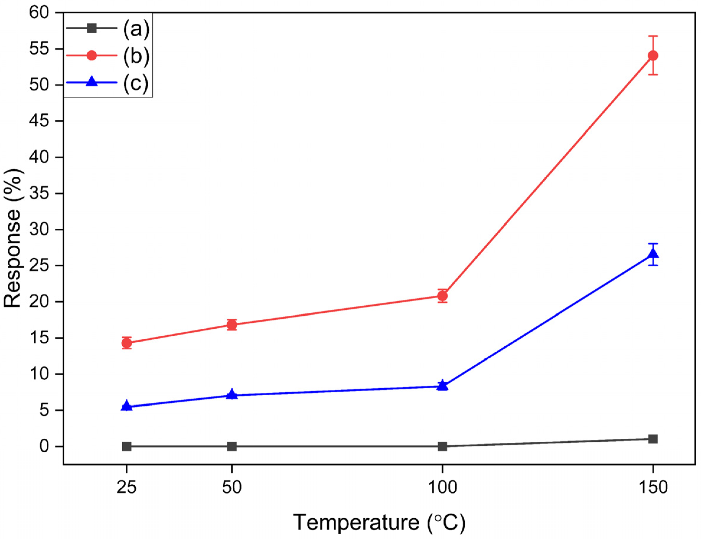
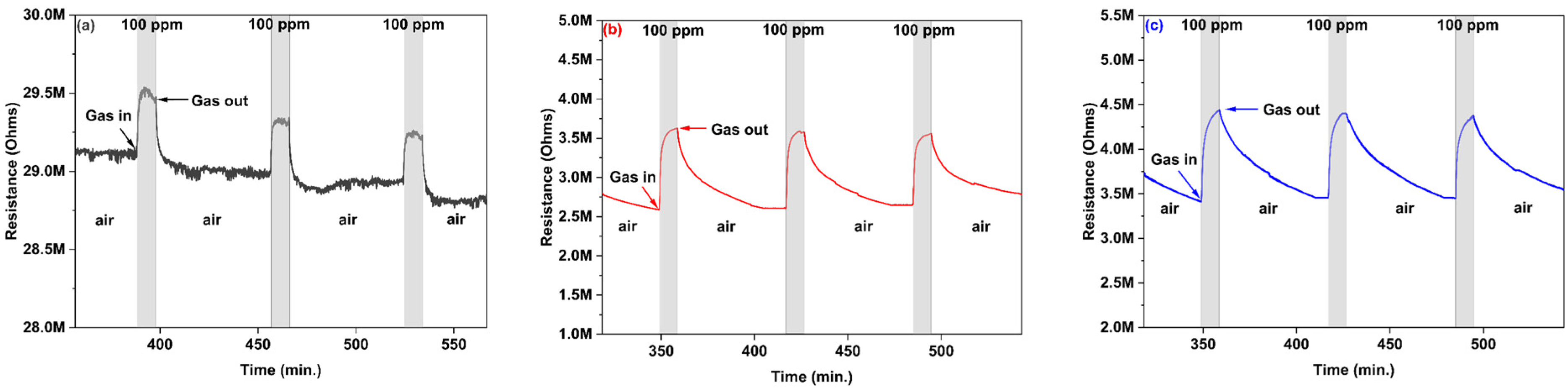
3.2.1. Hydrogen Gas Sensing

The gas sensing characteristics of pristine and Pd-decorated MoS2 thin films were analyzed to hydrogen gas. The sensor responses were checked at different operating temperatures (room temperature, 50 °C, 100 °C, and 150 °C) to study the optimal working temperature. Optimal temperature is an important parameter to define thermally active interactions between the target gas molecules and the adsorbed oxygen ionic species. Operating temperature plays an important role in determining the gas sensing performance of the sensors as it directly affects the selectivity, sensitivity, and response/recovery time. The desorption rate of the reacted by-products surpasses the adsorption rate of the target gas as temperature increases, reaching the peak efficiency at the optimal working temperature [61]. Figure 5 shows the sensor responses to 100 ppm H2 with respect to increases in temperature. The sensor responses increase with increases in the temperature, showing maximum response at 150 °C. Thus, the optimal working temperature of the sensors is 150 °C. The sensors were not operated beyond 150 °C to avoid the risk of oxidizing MoS2 to MoOx [62]. Indeed, based on our previous studies regarding the long-term stability of TMD-based gas sensors operated at temperatures equal to or below 150 °C, there were no remarkable changes in the material characteristics or the gas sensing performances. It is clear from the figure that there is a significant increase in the sensor response from pristine MoS2 to Pd-decorated MoS2, specifically in the case of MoS2-Pd_1. All three sensors showed reproducible responses. The sensor responses were calculated to be 55% at 150 °C to 100 ppm of H2 for MoS2-Pd_1, which is 1471% higher than the responses recorded in the case of pristine MoS2. Also, in the case of MoS2-Pd_2, the response is 300% higher than that for the pristine MoS2 sensor. As is evident from Figure 5, the minimum response recorded in the case of MoS2-Pd_1 is 14.3% at room temperature, which is 2760% higher than that of the pristine MoS2 under the same conditions. We can clearly observe the impact of Pd decoration on the sensitivity of the sensors to H2 gas. The main reason behind this increase in the sensitivity is the reaction between Pd and H2 atoms generating palladium hydride (PdHx) at room temperature [63,64] and also the affinity of MoS2 for H atoms [65]. Moreover, Pd nanoparticles have one of the highest sticking and diffusion coefficients [66]. Therefore, the results confirm the synergistic contribution of Pd and MoS2 for H2 sensing. The dynamics of resistance change and baseline recovery for all the sensors in a hydrogen environment as well as in synthetic air are shown in Figure 6. The amount of Pd decoration has a clear impact on the response of the sensors to hydrogen. Higher Pd coverage leads to the formation of more Schottky barriers, which, in turn, increases the resistance. In our case, we found the baseline resistance of the sensors with higher Pd decoration approximately 1 MΩ higher than the sensors with low Pd decoration (Figure 6b,c). When exposed to air, Pd tends to oxidize and form PdO nanoparticles, a p-type semiconductor. The decrease in the baseline resistance indicates that PdO nanoparticles inject holes in the MoS2 films. Moreover, excessive decoration of Pd on MoS2 impedes the transport efficiency of dissociated hydrogen atoms to the MoS2 channel, consequently hindering the catalytic effect. Furthermore, abundant Pd decoration leads to a reduction in the available surface area of MoS2 for interactions with hydrogen gas species owing to increased coverage by Pd nanoparticles. This results in lower sensing characteristics of the MoS2, suggesting lower Pd decoration amounts [41]. We compared our sensor responses with the highest-performing sensors in the literature based on noble metals and MoS2. Our sensors outperform the sensors in every aspect. Table 2 shows the comparison of our sensors with some highly responsive MoS2-based sensors for hydrogen sensing.
The increase in the electrical resistance values of the sensors upon exposure to hydrogen molecules (reducing gas) indicates the p-type nature of both the pristine and Pd-decorated sensors. Also, the sensors were exposed to increasing concentrations of H2 ranging from 50 ppm to 500 ppm in a background of dry air. Figure 7 show the resistance change dynamics of the sensors to increasing H2 pulses while being operated at 150 °C. As can be seen in the figure, the sensors responded well to the respective hydrogen concentrations with almost complete baseline recovery except in the case of pristine MoS2, which shows a slight drift. The sensors were able to detect a very low concentration of 50 ppm of H2 with excellent sensitivity. Rapid changes in the sensing signals exceeding final steady-state values can be seen in Figure 7b,c. This can be owed to the competition between reaction speed and gas diffusion [68,69,70]. The phenomenon is prominent when H2 concentration is high or Pd decoration is in excess. That is why this is much more prominent in the sensor with higher Pd content, as depicted in Figure 7c. To suppress this issue, when sensing higher concentrations of H2, thinner materials with high porosity can be helpful [63]. Figure 8 shows the sensor response as a function of the hydrogen concentration. The Pd-decorated sensor response values saturate above 100 ppm, and up to 100 ppm, the relationship between the sensor responses and the H2 concentration is quite linear. Also, the sensor responses with respect to H2 concentration in the case of pristine MoS2 are linear. It is worth mentioning that 100 ppm is much below the permissible limit for H2 gas for safety purposes. Palladium facilitates the dissociation of hydrogen molecules into chemisorbed hydrogen atoms (H) on its surface under ambient conditions without encountering any significant barriers. After their formation, these atoms quickly saturate the surface and migrate into interstitial lattice sites in the subsurface region before finally diffusing into the bulk. The diffusion of H atoms is impeded by an energy landscape characterized by subsurface sites that are energetically more favorable compared with bulk interstitials. Therefore, it is safe to assume that subsurface sites are occupied irrespective of the hydrogen concentration in the bulk. Additionally, it has been demonstrated that the presence of hydrogen in the subsurface layer can lead to the generation of lattice strain, which can impact the thermodynamics of the sorption process in nanoscale systems like nanoparticles [71].

3.2.2. Selectivity Test

In addition to H2 gas, the gas sensing performance of MoS2 and Pd-decorated MoS2 was investigated to reducing gases such as CO, NH3, ethanol, and benzene. Also, the sensor responses were investigated against an oxidizing gas: NO2. The typical resistance response dynamics for 5 ppm benzene, 80 ppm CO, 10 ppm ethanol, and 5 ppm NH3 are shown in Figures S2, S3, S4, and S5, respectively (supporting information). The histogram in Figure 9 summarizes the sensing results analyzed for each gas. Decorating MoS2 with Pd clearly enhances the response to H2 and diminishes cross-sensitivity to carbon monoxide, ammonia, benzene, and ethanol. However, all the sensors respond to NO2 with a significant response. It is worth mentioning and stressing that 800 ppb of NO2 is a very high concentration. The United States Environmental Protection Agency (U.S. EPA) has regulated the limit of exposure of NO2 at less than 100 ppb, keeping in view its negative effects both on the environment and human life [72]. For NO2 concentrations of 100 ppb, the sensor response is 18%. The pristine MoS2 demonstrates a robust response to NO2, while it lacks sensitivity to H2. By combining these two distinct sensors, we anticipate that the composite system can effectively mitigate the issue of cross-sensitivity displayed by Pd-decorated MoS2 to NO2. The complementary nature of the individual sensors, with pristine MoS2 being selective to NO2 and Pd-decorated MoS2 being responsive to H2, allows for a synergistic response that can enhance the discrimination capabilities of the composite sensor. This combination holds promise in suppressing the undesired cross-sensitivity exhibited by the Pd-decorated MoS2 sensor to NO2, enabling more accurate and reliable gas sensing applications. All the interfering species were tested at significantly higher concentrations; hence, it can be derived that Pd decoration improved selectivity to H2.
Ambient moisture affects the electrical properties of gas sensors dramatically and ultimately impacts the sensitivity heavily. This makes it mandatory to evaluate the behavior of the gas sensors in humid environments. Figure 10 depicts the sensor responses to 5 ppm of benzene (a reducing gas) under dry air and at 50% relative humidity (at 25 °C). Also, Figure S6 illustrates the normalized sensor resistance changes as a function of time. Analysis of the results reveals an overall decrease in the baseline resistance of the sensing layer when exposed to a humid environment. This has been reported in metal oxide semi-conducting materials as well [73]. We noticed a slight increase in the sensor responses, except in the MoS2-Pd_2 sensor. Generally, in humid environments, the water vapors (hydroxyl group) and the target gas molecules enter a competition at the active sites. The impact of the humidity is much more prominent when the relative surface distribution of the hydroxyl groups is much higher than the oxygen species [60]. The obtained results indicate that the sensors exhibit strong resilience to high levels of moisture.

3.2.3. Hydrogen Gas Sensing Mechanism

The sensing mechanism of chemoresistive gas sensors is based on electrical resistance modulation, which can be attributed to the interactions occurring on the sensor substrate because of the chemical reactions between the sensor surface and target gas [74]. When a sensor surface interacts with hydrogen, a reducing gas, it donates electrons upon adsorption. Depending on the type of the material (n-type or p-type), the transferred electrons lead to an increase or decrease in the electrical resistance of the material [39,40,75,76]. In this work, the resistance of MoS2 increased upon exposure to H2, indicating the p-type behavior of the material.
When the sensors are exposed to air, the oxygen molecules dissociate on the MoS2 surface, resulting in the formation of adsorbed oxygen species like ( O 2   a n d   O ) at elevated temperatures [39], as is shown in Equations (3) and (4).
O 2   g O 2 ( a d s )
O 2   ( a d s ) + e O 2   ( a d s )             100   ° C
Pd nanoparticle addition promotes the gas sensing ability of MoS2 by acting as an electronic sensitizer while sensing H2. Pd enhances the sensor responses by increasing the rate of chemical processes. One of the main roles of the Pd is to make catalytic oxidation easy on the MoS2 active layer [39]. When the sensors are exposed to hydrogen, the Pd nanoparticles provide adsorption sites for hydrogen molecules, as seen in Equation (5). Pd decoration enables barrierless dissociation of hydrogen molecules (H2) into chemisorbed hydrogen atoms (H) on its surface. The dissociation of the adsorbed hydrogen molecules takes place to form hydrogen atoms (Equation (6)). This process is known as the spillover effect of Pd catalysts with respect to H2 sensing [63]. For Pd particles larger than 5 to 10 nm (as in our case), the diffusion lengths for H atoms to reach the core are shorter [77]. The hydrogen atoms react with the  O  oxygen species (Equation (7)), facilitating the electrons to the sensor. These electrons combine with holes and reduce the charge carrier concentration, eventually leading to the increase in the sensor resistance. This increase is proportional to the concentration of hydrogen gas. These reactions are facilitated by the presence of Pd nanoparticles in the matrix owing to their strong affinity for the mitigation of chemisorbed gaseous species.
H 2   ( g a s )   2 H ( a d s )
H 2   ( a d s )   2 H ( a d s )
2 H ( a d s ) +   O ( a d s )   H 2 O + e

4. Conclusions

In this paper, layered MoS2 was successfully deposited onto alumina substrates. AACVD at 250 °C was employed for the Pd decoration of MoS2. The sensing material was well characterized using FESEM, XRD, HRTEM, and Raman spectroscopy. Multilayered crystalline MoS2 sheets were observed with homogenous Pd nanoparticle decoration. The size of the Pd nanoparticles was between 15 nm and 23 nm. The gas sensing results of bare and Pd-decorated MoS2 to H2 were analyzed. The Pd-nanoparticle-decorated MoS2 sensing layer acts as an active hydrogen-sensing layer with a maximum response of 55% at 150 °C to 100 ppm of H2. The sensors show high resilience to humidity, as the sensor responses increase slightly when exposed to 50% relative humidity. The effect of Pd decoration is evident with the sensitivity of the sensors depending on the amount of Pd decoration. A combined bare and Pd-decorated MoS2 sensor system holds promise for achieving a highly sensitive and selective H2 detection.

Supplementary Materials

The following supporting information can be downloaded at: https://www.mdpi.com/article/10.3390/chemosensors11110550/s1, Figure S1 depicts the thickness of the sensing layer, Figures S2–S5 show resistance dynamics towards interfering gases and Figure S6 shows normalized resistance dynamics in humid environment.

Author Contributions

Conceptualization, S.B.M.; Methodology, S.B.M. and F.E.A.; Validation, E.L.; Formal analysis, S.B.M.; Investigation, S.B.M. and F.E.A.; Writing—original draft, S.B.M.; Writing—review & editing, F.E.A.; Visualization, F.E.A.; Supervision, F.E.A. and E.L.; Funding acquisition, E.L. All authors have read and agreed to the published version of the manuscript.

Funding

This research was funded by Martí-Franquès Research grants Programme (Grant Number: 2019PMF-PIPF-14), Agencia Estatal de Investigación (Grant Number: TED2021-131442B-C31), and AGAUR (Grant Number: 2021 SGR 00147).

Institutional Review Board Statement

Not applicable.

Informed Consent Statement

Not applicable.

Data Availability Statement

Raw data is available from the authors upon request.

Acknowledgments

S.B.M is supported by the Martí-Franquès Research grant Programme, Doctoral grants—2019, (2019PMF-PIPF-14). F.E.A. is a Juan de la Cierva incorporacion Post-Doctoral Fellow. E.L. is supported by the Catalan Institution for Research and Advanced Studies via the 2018 Edition of the ICREA Academia Award. This work is supported by the Agencia Estatal de Investigación (AEI) under grant no. TED2021-131442B-C31 and by AGAUR under grant no. 2021 SGR 00147. The HRTEM was partially funded by the operative program FEDER Catalunya 2014-2020 (IU16-015844).

Conflicts of Interest

The authors declare no conflict of interest.

References

  1. Jacobson, M.Z.; Colella, W.G.; Golden, D.M. Cleaning the Air and Improving Health with Hydrogen Fuel-Cell Vehicles. Science 2005, 308, 1901–1905. [Google Scholar] [CrossRef] [PubMed]
  2. van Renssen, S. The hydrogen solution? Nat. Clim. Chang. 2020, 10, 799–801. [Google Scholar] [CrossRef]
  3. Agrawal, A.V.; Kumar, R.; Yang, G.; Bao, J.; Kumar, M.; Kumar, M. Enhanced adsorption sites in monolayer MoS2 pyramid structures for highly sensitive and fast hydrogen sensor. Int. J. Hydrog. Energy 2020, 45, 9268–9277. [Google Scholar] [CrossRef]
  4. Almaev, A.; Nikolaev, V.; Yakovlev, N.; Butenko, P.; Stepanov, S.; Pechnikov, A.; Scheglov, M.; Chernikov, E. Hydrogen sensors based on Pt/α-Ga2O3:Sn/Pt structures. Sens. Actuators B Chem. 2022, 364. [Google Scholar] [CrossRef]
  5. Gurlo, A. Nanosensors: Towards morphological control of gas sensing activity. SnO2, In2O3, ZnO and WO3 case studies. Nanoscale 2010, 3, 154–165. [Google Scholar] [CrossRef] [PubMed]
  6. Liu, X.; Ma, T.; Pinna, N.; Zhang, J. Two-Dimensional Nanostructured Materials for Gas Sensing. Adv. Funct. Mater. 2017, 27. [Google Scholar] [CrossRef]
  7. Raza, M.H.; Movlaee, K.; Leonardi, S.G.; Barsan, N.; Neri, G.; Pinna, N. Gas Sensing of NiO-SCCNT Core–Shell Heterostructures: Optimization by Radial Modulation of the Hole-Accumulation Layer. Adv. Funct. Mater. 2019, 30. [Google Scholar] [CrossRef]
  8. Zhang, J.; Liu, X.; Neri, G.; Pinna, N. Nanostructured Materials for Room-Temperature Gas Sensors. Adv. Mater. 2015, 28, 795–831. [Google Scholar] [CrossRef]
  9. Mai, H.D.; Jeong, S.; Nguyen, T.K.; Youn, J.-S.; Ahn, S.; Park, C.-M.; Jeon, K.-J. Pd Nanocluster/Monolayer MoS2 Heterojunctions for Light-Induced Room-Temperature Hydrogen Sensing. ACS Appl. Mater. Interfaces 2021, 13, 14644–14652. [Google Scholar] [CrossRef]
  10. Matte, H.S.S.R.; Gomathi, A.; Manna, A.K.; Late, D.J.; Datta, R.; Pati, S.K.; Rao, C.N.R. MoS2 and WS2 Analogues of Graphene. Angew. Chem. Int. Ed. 2010, 49, 4059–4062. [Google Scholar] [CrossRef]
  11. Lee, Y.-H.; Zhang, X.-Q.; Zhang, W.; Chang, M.-T.; Lin, C.-T.; Chang, K.-D.; Yu, Y.-C.; Wang, J.T.-W.; Chang, C.-S.; Li, L.-J.; et al. Synthesis of Large-Area MoS2Atomic Layers with Chemical Vapor Deposition. Adv. Mater. 2012, 24, 2320–2325. [Google Scholar] [CrossRef]
  12. Li, W.; Geng, X.; Guo, Y.; Rong, J.; Gong, Y.; Wu, L.; Zhang, X.; Li, P.; Xu, J.; Cheng, G.; et al. Reduced Graphene Oxide Electrically Contacted Graphene Sensor for Highly Sensitive Nitric Oxide Detection. ACS Nano 2011, 5, 6955–6961. [Google Scholar] [CrossRef] [PubMed]
  13. Lu, G.; E Ocola, L.; Chen, J. Reduced graphene oxide for room-temperature gas sensors. Nanotechnology 2009, 20, 445502. [Google Scholar] [CrossRef]
  14. Gutés, A.; Hsia, B.; Sussman, A.; Mickelson, W.; Zettl, A.; Carraro, C.; Maboudian, R. Graphene decoration with metal nanoparticles: Towards easy integration for sensing applications. Nanoscale 2011, 4, 438–440. [Google Scholar] [CrossRef] [PubMed]
  15. Hashtroudi, H.; Yu, A.; Juodkazis, S.; Shafiei, M. Two-Dimensional Dy2O3-Pd-PDA/rGO Heterojunction Nanocomposite: Synergistic Effects of Hybridisation, UV Illumination and Relative Humidity on Hydrogen Gas Sensing. Chemosensors 2022, 10, 78. [Google Scholar] [CrossRef]
  16. Geim, A.K.; Novoselov, K.S. The rise of graphene. Nat. Mater. 2007, 6, 183–191. [Google Scholar] [CrossRef]
  17. Radisavljevic, B.; Radenovic, A.; Brivio, J.; Giacometti, V.; Kis, A. Single-layer MoS2 transistors. Nat. Nanotechnol. 2011, 6, 147–150. [Google Scholar] [CrossRef]
  18. Sarkar, D.; Xie, X.; Kang, J.; Zhang, H.; Liu, W.; Navarrete, J.; Moskovits, M.; Banerjee, K. Functionalization of Transition Metal Dichalcogenides with Metallic Nanoparticles: Implications for Doping and Gas-Sensing. Nano Lett. 2015, 15, 2852–2862. [Google Scholar] [CrossRef]
  19. Xie, X.; Sarkar, D.; Liu, W.; Kang, J.; Marinov, O.; Deen, J.; Banerjee, K.; Engineering, C.; Barbara, S.; States, U. Low-Frequency Noise in Bilayer MoS2. ACS Nano 2014, 8, 5633–5640. [Google Scholar] [CrossRef]
  20. Siao, M.D.; Shen, W.C.; Chen, R.S.; Chang, Z.W.; Shih, M.C.; Chiu, Y.P.; Cheng, C.-M. Two-dimensional electronic transport and surface electron accumulation in MoS2. Nat. Commun. 2018, 9, 1–12. [Google Scholar] [CrossRef]
  21. Mennel, L.; Furchi, M.M.; Wachter, S.; Paur, M.; Polyushkin, D.K.; Mueller, T. Optical imaging of strain in two-dimensional crystals. Nat. Commun. 2018, 9, 516. [Google Scholar] [CrossRef] [PubMed]
  22. Eda, G.; Yamaguchi, H.; Voiry, D.; Fujita, T.; Chen, M.; Chhowalla, M. Photoluminescence from Chemically Exfoliated MoS2. Nano Lett. 2011, 11, 5111–5116. [Google Scholar] [CrossRef] [PubMed]
  23. Winkler, C.; Harivyasi, S.S.; Zojer, E. Controlling the electronic properties of van der Waals heterostructures by applying electrostatic design. 2D Mater. 2018, 5, 035019. [Google Scholar] [CrossRef]
  24. Liao, F.; Guo, Z.; Wang, Y.; Xie, Y.; Zhang, S.; Sheng, Y.; Tang, H.; Xu, Z.; Riaud, A.; Zhou, P.; et al. High-Performance Logic and Memory Devices Based on a Dual-Gated MoS2 Architecture. ACS Appl. Electron. Mater. 2019, 2, 111–119. [Google Scholar] [CrossRef]
  25. Yu, S.H.; Lee, Y.B.; Jang, S.K.; Kang, J.; Jeon, J.; Lee, C.G.; Lee, J.Y.; Kim, H.; Hwang, E.; Lee, S.; et al. Dye-Sensitized MoS2 Photodetector with Enhanced Spectral Photoresponse. ACS Nano 2014, 8, 8285–8291. [Google Scholar] [CrossRef]
  26. Gan, L.-Y.; Zhang, Q.; Cheng, Y.; Schwingenschlögl, U. Photovoltaic Heterojunctions of Fullerenes with MoS2 and WS2 Monolayers. J. Phys. Chem. Lett. 2014, 5, 1445–1449. [Google Scholar] [CrossRef]
  27. Kuru, C.; Choi, C.; Kargar, A.; Choi, D.; Kim, Y.J.; Liu, C.H.; Yavuz, S.; Jin, S. MoS2 Nanosheet–Pd Nanoparticle Composite for Highly Sensitive Room Temperature Detection of Hydrogen. Adv. Sci. 2015, 2, 1500004. [Google Scholar] [CrossRef]
  28. Tabata, H.; Matsuyama, H.; Goto, T.; Kubo, O.; Katayama, M. Visible-Light-Activated Response Originating from Carrier-Mobility Modulation of NO2 Gas Sensors Based on MoS2 Monolayers. ACS Nano 2021, 15, 2542–2553. [Google Scholar] [CrossRef]
  29. Bai, J.; Shen, Y.; Zhao, S.; Chen, Y.; Li, G.; Han, C.; Wei, D.; Yuan, Z.; Meng, F. Flower-like MoS2 hierarchical architectures assembled by 2D nanosheets sensitized with SnO2 quantum dots for high-performance NH3 sensing at room temperature. Sens. Actuators B Chem. 2021, 353, 131191. [Google Scholar] [CrossRef]
  30. Hou, S.; Pang, R.; Chang, S.; Ye, L.; Xu, J.; Wang, X.-C.; Zhang, Y.; Shang, Y.; Cao, A. Synergistic CNFs/CoS2/MoS2 Flexible Films with Unprecedented Selectivity for NO Gas at Room Temperature. ACS Appl. Mater. Interfaces 2020, 12, 29778–29786. [Google Scholar] [CrossRef]
  31. Lee, K.; Gatensby, R.; McEvoy, N.; Hallam, T.; Duesberg, G.S. High-Performance Sensors Based on Molybdenum Disulfide Thin Films. Adv. Mater. 2013, 25, 6699–6702. [Google Scholar] [CrossRef] [PubMed]
  32. Liu, B.; Chen, L.; Liu, G.; Abbas, A.N.; Fathi, M.; Zhou, C. High-Performance Chemical Sensing Using Schottky-Contacted Chemical Vapor Deposition Grown Monolayer MoS2 Transistors. ACS Nano 2014, 8, 5304–5314. [Google Scholar] [CrossRef] [PubMed]
  33. Li, H.; Yin, Z.; He, Q.; Li, H.; Huang, X.; Lu, G.; Fam, D.W.H.; Tok, A.I.Y.; Zhang, Q.; Zhang, H. Fabrication of Single- and Multilayer MoS2 Film-Based Field-Effect Transistors for Sensing NO at Room Temperature. Small 2011, 8, 63–67. [Google Scholar] [CrossRef]
  34. Zhou, Q.; Hong, C.; Yao, Y.; Hussain, S.; Xu, L.; Zhang, Q.; Gui, Y.; Wang, M. Hierarchically MoS2 nanospheres assembled from nanosheets for superior CO gas-sensing properties. Mater. Res. Bull. 2018, 101, 132–139. [Google Scholar] [CrossRef]
  35. Ozaki, F.; Tanaka, S.; Osada, W.; Mukai, K.; Horio, M.; Koitaya, T.; Yamamoto, S.; Matsuda, I.; Yoshinobu, J. Functionalization of the MoS2 basal plane for activation of molecular hydrogen by Pd deposition. Appl. Surf. Sci. 2022, 593. [Google Scholar] [CrossRef]
  36. Alagh, A.; Annanouch, F.E.; Umek, P.; Bittencourt, C.; Colomer, J.F.; Llobet, E. An Ultrasensitive Room-Temperature H2S Gas Sensor Based on 3D Assembly of Cu2O Decorated WS2 Nanomaterial. IEEE Sens. J. 2021, 21, 21212–21220. [Google Scholar] [CrossRef]
  37. Annanouch, F.E.; Haddi, Z.; Ling, M.; di Maggio, F.; Vallejos, S.; Vilic, T.T.; Zhu, Y.; Shujah, T.; Umek, P.; Bittencourt, C.; et al. Aerosol-Assisted CVD-Grown PdO Nanoparticle-Decorated Tungsten Oxide Nanoneedles Extremely Sensitive and Selective to Hydrogen. ACS Appl. Mater. Interfaces 2016, 8, 10413–10421. [Google Scholar] [CrossRef]
  38. Baek, D.-H.; Kim, J. MoS2 gas sensor functionalized by Pd for the detection of hydrogen. Sens. Actuators B Chem. 2017, 250, 686–691. [Google Scholar] [CrossRef]
  39. Gottam, S.R.; Tsai, C.-T.; Wang, L.-W.; Wang, C.-T.; Lin, C.-C.; Chu, S.-Y. Highly sensitive hydrogen gas sensor based on a MoS2-Pt nanoparticle composite. Appl. Surf. Sci. 2019, 506, 144981. [Google Scholar] [CrossRef]
  40. Urs, K.M.B.; Katiyar, N.K.; Kumar, R.; Biswas, K.; Singh, A.K.; Tiwary, C.S.; Kamble, V. Multi-component (Ag–Au–Cu–Pd–Pt) alloy nanoparticle-decorated p-type 2D-molybdenum disulfide (MoS2) for enhanced hydrogen sensing. Nanoscale 2020, 12, 11830–11841. [Google Scholar] [CrossRef]
  41. Lee, J.-H.; Mirzaei, A.; Kim, J.-Y.; Kim, J.-H.; Kim, H.W.; Kim, S.S. Optimization of the surface coverage of metal nanoparticles on nanowires gas sensors to achieve the optimal sensing performance. Sens. Actuators B Chem. 2019, 302, 127196. [Google Scholar] [CrossRef]
  42. Lee, J.-S.; Katoch, A.; Kim, J.-H.; Kim, S.S. Effect of Au nanoparticle size on the gas-sensing performance of p-CuO nanowires. Sens. Actuators B Chem. 2016, 222, 307–314. [Google Scholar] [CrossRef]
  43. Kim, S.S.; Park, J.Y.; Choi, S.-W.; Kim, H.S.; Gil Na, H.; Yang, J.C.; Lee, C.; Kim, H.W. Room temperature sensing properties of networked GaN nanowire sensors to hydrogen enhanced by the Ga2Pd5 nanodot functionalization. Int. J. Hydrog. Energy 2011, 36, 2313–2319. [Google Scholar] [CrossRef]
  44. Stolze, M.; Gogova, D.; Thomas, L.-K. Analogy for the maximum obtainable colouration between electrochromic, gasochromic, and electrocolouration in DC-sputtered thin WO3−y films. Thin Solid Films 2005, 476, 185–189. [Google Scholar] [CrossRef]
  45. Hwang, I.-S.; Choi, J.-K.; Woo, H.-S.; Kim, S.-J.; Jung, S.-Y.; Seong, T.-Y.; Kim, I.-D.; Lee, J.-H. Facile Control of C2H5OH Sensing Characteristics by Decorating Discrete Ag Nanoclusters on SnO2 Nanowire Networks. ACS Appl. Mater. Interfaces 2011, 3, 3140–3145. [Google Scholar] [CrossRef] [PubMed]
  46. Late, D.J.; Huang, Y.-K.; Liu, B.; Acharya, J.; Shirodkar, S.N.; Luo, J.; Yan, A.; Charles, D.; Waghmare, U.V.; Dravid, V.P.; et al. Sensing Behavior of Atomically Thin-Layered MoS2 Transistors. ACS Nano 2013, 7, 4879–4891. [Google Scholar] [CrossRef]
  47. Eom, T.H.; Cho, S.H.; Suh, J.M.; Kim, T.; Lee, T.H.; Jun, S.E.; Yang, J.W.; Lee, J.; Hong, S.-H.; Jang, H.W. Substantially improved room temperature NO2 sensing in 2-dimensional SnS2 nanoflowers enabled by visible light illumination. J. Mater. Chem. A 2021, 9, 11168–11178. [Google Scholar] [CrossRef]
  48. Park, J.; Mun, J.; Shin, J.-S.; Kang, S.-W. Highly sensitive two-dimensional MoS2 gas sensor decorated with Pt nanoparticles. R. Soc. Open Sci. 2018, 5, 181462. [Google Scholar] [CrossRef]
  49. Suh, J.M.; Shim, Y.-S.; Kwon, K.C.; Jeon, J.-M.; Lee, T.H.; Shokouhimehr, M.; Jang, H.W. Pd- and Au-Decorated MoS2 Gas Sensors for Enhanced Selectivity. Electron. Mater. Lett. 2019, 15, 368–376. [Google Scholar] [CrossRef]
  50. Burman, D.; Raha, H.; Manna, B.; Pramanik, P.; Guha, P.K. Substitutional Doping of MoS2 for Superior Gas-Sensing Applications: A Proof of Concept. ACS Sens. 2021, 6, 3398–3408. [Google Scholar] [CrossRef]
  51. Huang, X.; Zeng, Z.; Bao, S.; Wang, M.; Qi, X.; Fan, Z.; Zhang, H. Solution-phase epitaxial growth of noble metal nanostructures on dispersible single-layer molybdenum disulfide nanosheets. Nat. Commun. 2013, 4, 1444. [Google Scholar] [CrossRef] [PubMed]
  52. Kim, T.; Lee, T.H.; Park, S.Y.; Eom, T.H.; Cho, I.; Kim, Y.; Kim, C.; A Lee, S.; Choi, M.-J.; Suh, J.M.; et al. Drastic Gas Sensing Selectivity in 2-Dimensional MoS2 Nanoflakes by Noble Metal Decoration. ACS Nano 2023, 17, 4404–4413. [Google Scholar] [CrossRef] [PubMed]
  53. Lee, S.; Kang, Y.; Lee, J.; Kim, J.; Shin, J.W.; Sim, S.; Go, D.; Jo, E.; Kye, S.; Kim, J.; et al. Atomic layer deposited Pt nanoparticles on functionalized MoS2 as highly sensitive H2 sensor. Appl. Surf. Sci. 2021, 571, 151256. [Google Scholar] [CrossRef]
  54. Alagh, A.; Annanouch, F.E.; Al Youssef, K.; Bittencourt, C.; Güell, F.; Martínez-Alanis, P.R.; Reguant, M.; Llobet, E. PdO and PtO loaded WS2 boosts NO2 gas sensing characteristics at room temperature. Sens. Actuators B Chem. 2022, 364. [Google Scholar] [CrossRef]
  55. Alagh, A.; Annanouch, F.E.; Umek, P.; Bittencourt, C.; Sierra-Castillo, A.; Haye, E.; Colomer, J.F.; Llobet, E. CVD growth of self-assembled 2D and 1D WS2 nanomaterials for the ultrasensitive detection of NO2. Sens. Actuators B Chem. 2020, 326, 128813. [Google Scholar] [CrossRef]
  56. Li, S.; Wang, S.; Salamone, M.M.; Robertson, A.W.; Nayak, S.; Kim, H.; Tsang, S.C.E.; Pasta, M.; Warner, J.H. Edge-Enriched 2D MoS2 Thin Films Grown by Chemical Vapor Deposition for Enhanced Catalytic Performance. ACS Catal. 2016, 7, 877–886. [Google Scholar] [CrossRef]
  57. Shomalian, K.; Bagheri-Mohagheghi, M.-M.; Ardyanian, M. Characterization and study of reduction and sulfurization processing in phase transition from molybdenum oxide (MoO2) to molybdenum disulfide (MoS2) chalcogenide semiconductor nanoparticles prepared by one-stage chemical reduction method. Appl. Phys. A 2016, 123, 93. [Google Scholar] [CrossRef]
  58. Ramakrishnan, V.; Alex, C.; Nair, A.N.; John, N.S. Designing Metallic MoO2 Nanostructures on Rigid Substrates for Electrochemical Water Activation. Chem.–A Eur. J. 2018, 24, 18003–18011. [Google Scholar] [CrossRef]
  59. Lee, C.; Yan, H.; Brus, L.E.; Heinz, T.F.; Hone, J.; Ryu, S. Anomalous Lattice Vibrations of Single- and Few-Layer MoS2. ACS Nano 2010, 4, 2695–2700. [Google Scholar] [CrossRef]
  60. Annanouch, F.E.; Alagh, A.; Umek, P.; Casanova-Chafer, J.; Bittencourt, C.; Llobet, E. Controlled growth of 3D assemblies of edge enriched multilayer MoS2 nanosheets for dually selective NH3 and NO2 gas sensors. J. Mater. Chem. C 2022, 10, 11027–11039. [Google Scholar] [CrossRef]
  61. Bendahan, M.; Guérin, J.; Boulmani, R.; Aguir, K. WO3 sensor response according to operating temperature: Experiment and modeling. Sens. Actuators B Chem. 2007, 124, 24–29. [Google Scholar] [CrossRef]
  62. Park, S.; Garcia-Esparza, A.T.; Abroshan, H.; Abraham, B.; Vinson, J.; Gallo, A.; Nordlund, D.; Park, J.; Kim, T.R.; Vallez, L.; et al. Operando Study of Thermal Oxidation of Monolayer MoS2. Adv. Sci. 2021, 8, 2002768. [Google Scholar] [CrossRef] [PubMed]
  63. Park, C.H.; Koo, W.-T.; Lee, Y.J.; Kim, Y.H.; Lee, J.; Jang, J.-S.; Yun, H.; Kim, I.-D.; Kim, B.J. Hydrogen Sensors Based on MoS2 Hollow Architectures Assembled by Pickering Emulsion. ACS Nano 2020, 14, 9652–9661. [Google Scholar] [CrossRef] [PubMed]
  64. Kowalska, E.; Czerwosz, E.; Diduszko, R.; Kaminska, A.; Danila, M. Influence of PdHx formation ability on hydrogen sensing properties of palladium-carbonaceous films. Sens. Actuators A Phys. 2013, 203, 434–440. [Google Scholar] [CrossRef]
  65. Huang, Z.; Luo, W.; Ma, L.; Yu, M.; Ren, X.; He, M.; Polen, S.; Click, K.; Garrett, B.; Lu, J.; et al. Dimeric [Mo2S12]2−Cluster: A Molecular Analogue of MoS2 Edges for Superior Hydrogen-Evolution Electrocatalysis. Angew. Chem. Int. Ed. 2015, 54, 15181–15185. [Google Scholar] [CrossRef]
  66. Tang, X.; Haddad, P.-A.; Mager, N.; Geng, X.; Reckinger, N.; Hermans, S.; Debliquy, M.; Raskin, J.-P. Chemically deposited palladium nanoparticles on graphene for hydrogen sensor applications. Sci. Rep. 2019, 9, 1–11. [Google Scholar] [CrossRef]
  67. Jaiswal, J.; Tiwari, P.; Singh, P.; Chandra, R. Fabrication of highly responsive room temperature H2 sensor based on vertically aligned edge-oriented MoS2 nanostructured thin film functionalized by Pd nanoparticles. Sens. Actuators B Chem. 2020, 325. [Google Scholar] [CrossRef]
  68. Matsunaga, N.; Sakai, G.; Shimanoe, K.; Yamazoe, N. Diffusion equation-based study of thin film semiconductor gas sensor-response transient. Sens. Actuators B Chem. 2002, 83, 216–221. [Google Scholar] [CrossRef]
  69. Matsunaga, N.; Sakai, G.; Shimanoe, K.; Yamazoe, N. Formulation of gas diffusion dynamics for thin film semiconductor gas sensor based on simple reaction–diffusion equation. Sens. Actuators B Chem. 2003, 96, 226–233. [Google Scholar] [CrossRef]
  70. Suresh, S.; Urs, K.M.B.; Vasudevan, A.T.; Sriram, S.; Kamble, V.B. Analysis of Unusual and Instantaneous Overshoot of Response Transients in Gas Sensors. Phys. Status Solidi (RRL)–Rapid Res. Lett. 2019, 13. [Google Scholar] [CrossRef]
  71. Darmadi, I.; Nugroho, F.A.A.; Langhammer, C. High-Performance Nanostructured Palladium-Based Hydrogen Sensors—Current Limitations and Strategies for Their Mitigation. ACS Sens. 2020, 5, 3306–3327. [Google Scholar] [CrossRef]
  72. Wang, J.; Yang, Y.; Xia, Y. Mesoporous MXene/ZnO nanorod hybrids of high surface area for UV-activated NO2 gas sensing in ppb-level. Sens. Actuators B Chem. 2022, 353. [Google Scholar] [CrossRef]
  73. Rsan, N.B.; Weimar, U. Understanding the fundamental principles of metal oxide based gas sensors; the example of CO sensing with SnO2 sensors in the presence of humidity. J. Phys. Condens. Matter 2003, 15, R813–R839. [Google Scholar] [CrossRef]
  74. Hashtroudi, H.; Atkin, P.; Mackinnon, I.D.R.; Shafiei, M. Low-operating temperature resistive nanostructured hydrogen sensors. Int. J. Hydrog. Energy 2019, 44, 26646–26664. [Google Scholar] [CrossRef]
  75. Mirzaei, A.; Yousefi, H.R.; Falsafi, F.; Bonyani, M.; Lee, J.-H.; Kim, J.-H.; Kim, H.W.; Kim, S.S. An overview on how Pd on resistive-based nanomaterial gas sensors can enhance response toward hydrogen gas. Int. J. Hydrog. Energy 2019, 44, 20552–20571. [Google Scholar] [CrossRef]
  76. Chacko, L.; Massera, E.; Aneesh, P.M. Enhancement in the Selectivity and Sensitivity of Ni and Pd Functionalized MoS2 Toxic Gas Sensors. J. Electrochem. Soc. 2020, 167, 106506. [Google Scholar] [CrossRef]
  77. Asakuma, Y.; Miyauchi, S.; Yamamoto, T.; Aoki, H.; Miura, T. Numerical analysis of absorbing and desorbing mechanism for the metal hydride by homogenization method. Int. J. Hydrog. Energy 2003, 28, 529–536. [Google Scholar] [CrossRef]
Figure 1. FESEM images of (a) MoS2, (b) MoS2-Pd_1, and (c) MoS2-Pd_2.
Chemosensors 11 00550 g001
Figure 2. (a) TEM image of multilayer MoS2_Pd, (b) color mapping of MoS2_Pd, (c) EDX pattern of MoS2_Pd, (d) HRTEM image of multilayer pristine MoS2 with d-spacing of 0.215 nm, (e) close-up of Pd nanoparticle with d-spacing 0.232 nm.
Chemosensors 11 00550 g002
Figure 3. XRD diffractogram of (a) MoS2, (b) MoS2-Pd_1, and (c) MoS2-Pd_2.
Chemosensors 11 00550 g003
Figure 4. Raman spectra of (a) MoS2, (b) MoS2-Pd_1, and (c) MoS2-Pd_2.
Chemosensors 11 00550 g004
Figure 5. Sensor responses as a function of temperature to 100 ppm H2, (a) MoS2, (b) MoS2-Pd_1, and (c) MoS2-Pd_2.
Chemosensors 11 00550 g005
Figure 6. Sensor resistance dynamics (a) MoS2, (b) MoS2-Pd_1, and (c) MoS2-Pd_2 to 100 ppm H2 at 150 °C.
Chemosensors 11 00550 g006
Figure 7. Sensor responses to increasing concentration of H2 at 150 °C (a) MoS2, (b) MoS2-Pd_1, and (c) MoS2-Pd_2.
Chemosensors 11 00550 g007
Figure 8. Calibration curves to H2 for the different types of sensors tested. Sensors operated at 150 °C, (a) MoS2, (b) MoS2-Pd_1, and (c) MoS2-Pd_2.
Chemosensors 11 00550 g008
Figure 9. Response histogram of MoS2, MoS2-Pd_1, and MoS2-Pd_2 to NO2 (800 ppb), H2 (100 ppm), ethanol (10 ppm), carbon monoxide (80 ppm), ammonia (5 ppm), and benzene (5 ppm) at 150 °C.
Chemosensors 11 00550 g009
Figure 10. Sensor responses to 5 ppm benzene at 150 °C.
Chemosensors 11 00550 g010
Table 1. Summary of Raman data.
Sample   E 2 g 1   A 1 g Δ = ( A 1 g E 2 g 1 )
MoS238140625
MoS2-Pd_138140726
MoS2-Pd_237840527
Table 2. Hydrogen gas sensing comparison of various noble metal-doped/decorated MoS2 sensors.
Gas Sensing MaterialConcentrationResponse Calculation FormulaResponse %Operating TemperatureReference
ALD Pt-decorated MoS2 nanosheets1000 ppm   R a i r R H 2 440250 °C[53]
Pd nanoclusters–MoS2 heterostructure140 ppm   R H 2 R a i r R a i r × 100 17RT (with light activation)[9]
Pd-functionalized MoS2 nanosheet10,000 ppm R H 2 R a i r R a i r × 10035.3RT[38]
Pt-decorated MoS2 hollow structures40,000 ppm R H 2 R a i r R a i r × 10011.2RT[63]
Pd-functionalized edge-enriched MoS2500 ppm   R H 2 R a i r R a i r × 100 33.7RT[67]
Pd-decorated MoS2100 ppm   R H 2 R a i r R a i r × 100 55150 °CThis work
14.9RT
Disclaimer/Publisher’s Note: The statements, opinions and data contained in all publications are solely those of the individual author(s) and contributor(s) and not of MDPI and/or the editor(s). MDPI and/or the editor(s) disclaim responsibility for any injury to people or property resulting from any ideas, methods, instructions or products referred to in the content.

