Article

Characterization of Flexible Copper Selenide Films on Polyamide Substrate Obtained by SILAR Method—Towards Application in Electronic Devices

1
Department of Physical and Inorganic Chemistry, Kaunas University of Technology, Radvilenu 19, 50254 Kaunas, Lithuania
2
Institute of Physics Belgrade, University of Belgrade, Pregrevica 118, 11080 Belgrade, Serbia
3
Institut of Experimental Physics, Freie Universität Berlin, Arnimallee 14, 14195 Berlin, Germany
4
Institute for Multidisciplinary Research, University of Belgrade, Kneza Viseslava 1, 11000 Belgrade, Serbia
*
Author to whom correspondence should be addressed.
Chemosensors 2022, 10(8), 313; https://doi.org/10.3390/chemosensors10080313
Submission received: 22 June 2022 / Revised: 28 July 2022 / Accepted: 1 August 2022 / Published: 5 August 2022
(This article belongs to the Special Issue Nanomaterials-Based Sensors)

Abstract

:
Thin copper selenide films were synthesized on polyamide sheets using the successive ionic layer adsorption and reaction (SILAR) method at three different temperatures. It was found that elevating the temperature of the solution led to the creation of copper selenide films with different features. X-ray diffraction characterization revealed that all films crystallized into a cubic Cu2−xSe, but with different crystallinity parameters. With elevating the temperature, grain size increased (6.61–14.33 and 15.81 for 40, 60 and 80 °C, respectively), while dislocation density and the strain decreased. Surface topology was investigated with Scanning Electron Microscopy and Atomic Force Microscopy, which revealed that the grains combined into agglomerates of up to 100 nm (80 °C) to 1 μm (40 °C). The value of the direct band gap of the copper selenide thin films, obtained with UV/VIS spectroscopy, varied in the range of 2.28–1.98 eV. The formation of Cu2−xSe was confirmed by Raman analysis; the most prominent Raman peak is located at 260 cm−1, which is attributed to binary copper selenides. The thin Cu2−xSe films deposited on polyamide showed p-type conductivity, and the electrical resistivity varied in the range of 20–50 Ω. Our results suggest that elevated temperatures prevent large agglomeration, leading to higher resistance behavior.

1. Introduction

Copper selenide can be formed in various stoichiometric compositions, such as CuSe, Cu2Se, CuSe2, Cu3Se2, Cu7Se4, Cu5Se4, Cu3Se4, and non-stoichiometric compositions Cu2−xSe [1,2,3]. The stoichiometric composition of copper selenide strongly influenced its crystalline structure and electronic behavior—it alters its electronic, chemical, and thermal properties [4,5]. Copper-deficient Cu2−xSe is an intrinsic p-type semiconductor with direct bandgap energies in the range of 2.0 to 2.4 eV, the work function of 4.17 eV, and high photo-electrochemical conversion efficiency (~14.6%) [3,5,6,7,8]. These features of Cu2−xSe can be used as Shottky diodes [9], self-repairable electrodes [10], and photovoltaic devices [8]. Furthermore, the Cu2−xSe columnar superstructures are used as low-cost and highly efficient counter electrodes in quantum dot sensitized solar cells [11,12].
Several decades ago, due to concerns about homeland security, medical and environmental monitoring as well as food safety, a large interest was shown in the development of gas sensors for detecting volatile and toxic gases. Cu2−xSe exhibits good sensitivity and short response and recovery times to Hg2+ [13], and organic gases such as ethanol and acetone [14].
Many works have been reported on the formation of Cu2−xSe on substrates, such as glass [1,6,15], and fluorine-doped tin oxide [8,11,12,16].
Flexible electronics is a growing field that is promising to develop various new commercial products such as displays, solar cells, flexible photovoltaics, and biomedical sensors due to their lightweight and low cost [17,18,19,20,21]. Flexible polymer substrates possess unique features such as low cost, low thickness, low mass, and excellent mechanical deformability. They can remain in the environmental, chemical, and thermal environments required for the construction of electronic circuits while maintaining their mechanical flexibility [22,23]. Recently, ferroelectric semiconductors have been increasingly studied [24,25].
When Cu2−xSe is deposited on a flexible transparent polymer substrate (polyvinylchloride, polyvinyl alcohol), the possibility of using thin flexible polymer substrates appears in the fabrication of flexible optoelectronic devices [26]. Cu2−xSe films on polyester sheets can be used as a transparent electrode for inorganic and organic hybrid light emitters, as a possible replacement for indium tin oxide or fluorine-doped tin oxide [7].
This work reports the preparation and characterization of electrically conductive copper selenide onto polyamide 6 (PA) sheets. Polyamide 6 was chosen as a cheap, chemically stable, and flexible substrate. Flexibility is the ability of the material to be bent without mechanical failures such as fracture and plastic deformation. One of the few mechanical parameters that describe the deformation of a material is Young’s modulus, which characterizes the resistance of a material to elastic deformation. Young’s moduli of polyamide 6 are lower than those of other polymers. For example, polyimide and polyethylene terephthalate have a Young’s modulus of 4 GPa and 3 GPa, respectively, while the Young’s modulus of polyamide 6 is 2.4 GPa [17,27,28]. As a semihydrophilic flexible polymer, PA is capable of adsorbing molecules or ions of various electrolytes from nonaqueous and aqueous solutions [29,30]. Unlike glass and fluorine-doped tin oxide substrates, on which copper selenide builds a thin film, polymer allows the material to partially diffuse in it, so the final product is a conductive composite (PA with copper selenide nanocrystals embedded in it).
Cu2−xSe films can be prepared by chemical bath deposition [1,7,31], combined electrochemical followed by chemical bath deposition [8], sonochemical synthesis [32], ion beam sputtering deposition [33], electrochemical [12], successive ionic layer adsorption and reaction [15,34], and other methods.
Here, copper selenide nanocrystals were formed on the surface as well as inside the polyamide using the simple and versatile successive ionic layer adsorption and reaction (SILAR) method. The method used differs from other chemical methods, as it does not require specialized equipment or conditions; it is quite inexpensive and simple, convenient for large area deposition, and it can be used at room temperature [34]. As a low-temperature process, it also avoids oxidation [35]. The SILAR method consists of two stages: first, copper ions are adsorbed on the polyamide surface from a precursor solution containing copper ions; second, copper selenide thin films are formed by treating the layer formed in the first stage with a solution containing selenium ions. To the best of our knowledge, the copper selenide/PA composite by employing the SILAR method has never been obtained before. We suggest that slightly elevated solution temperatures could facilitate crystalline formation in the polymer matrix and therefore improve the optical and electric properties of the as-obtained composites. Combined with the natural abundance of material and the low cost of composite production, the copper selenide/PA composite could be a possibility for printable electronics on flexible substrates or in sensors in the future.
Structural characterization of the composites was performed with the help of X-ray diffraction, Scanning electron microscopy combined with Energy-dispersive X-ray spectroscopy, and Raman Spectroscopy, while the optical properties were characterized with UV/VIS spectroscopy. The surface morphology of the films was investigated with Atomic Force Microscopy. The conductivity of the composites was checked with a multimeter.

2. Materials and Methods

2.1. Materials and Film Preparation

The reactive solutions were made with just pure analytical reagents and purified water. All reagents were obtained from Sigma-Aldrich and used as received. Only freshly prepared solutions were used for experiments and were not de-aerated during the experiments.
Thin copper selenide films were deposited on a PA sheet (PA 6, Tecamid 6, density 1.13 g/cm−3, thickness 500 μm, surface resistance ~1 kΩ/m2), which was obtained from Ensinger GmbH (Germany). Before the experiments, the PA films were boiled in distilled water for 2 h to remove the remaining unpolymerized monomer residues. Then, they were dried with filter paper and incubated over anhydrous CaCl2 for 24 h.
The copper sulfate solution (CuSO4) was used as the cationic solution and the freshly prepared sodium selenosulfate solution (Na2SeSO3) was used as the anionic solution for the deposition of a thin film of copper selenide on PA using the SILAR method.
To prepare the Na2SeSO3 solution, selenium powder (99% purity) and anhydrous sodium sulfite were dissolved in distilled water for 8 h at 80 °C with constant stirring. It was kept for 24 h in a sealed container, to allow undissolved selenium to settle. A clear solution was obtained after it was filtered [34].
In one SILAR cycle, the substrate was immersed separately in solutions of anionic and cationic precursors. The substrate was washed with an ion exchange solution (distilled water) to avoid a homogeneous deposition between each immersion.
Thin copper selenide films on polyamide substrate were grown by repeating these cycles 30 times at different temperatures (40 °C, 60 °C, and 80 °C). The proposed reaction mechanism of the obtained film could be found in [34].

2.2. Characterization of Copper Selenide Films

X-ray diffraction (XRD) measurements were performed using a Philips PW 1050 diffractometer equipped with a PW 1730 generator, 40 kV × 20 mA, using Ni filtered Co Kα radiation of 0.1778897 nm at room temperature. Measurements were carried out in the 2 h range of 10 to 70° with a scanning step of 0.05° and a scan time of 10 s per step. The experimental values of d (lattice spacing) for copper selenide are determined using the Bragg relation [36]. The average grain size (D) was calculated based on the full width at the half-maximum intensity (FWHM) of the main reflections by applying Scherrer’s formula [37,38]. Furthermore, to have more information on the number of defects in the films, the dislocation density (δ) [34] and the strain (ε) values were calculated [39].
Scanning electron microscopy (SEM) was performed using a Raith GMBH e-Line instrument equipped with a field emission gun operating at 10 kV accelerating voltage, magnification: 20,000 k. A secondary electron signal was used for imaging. Energy-dispersive X-ray spectroscopy (EDX) imaging was performed using QUANTAX EDS with an X-Flash Detector 3001 and ESPRIT software.
The UV/VIS absorbance and diffusion reflectance spectra were recorded in the wavelength range of 200–800 nm on a Shimadzu UV-2600 spectrophotometer equipped with an integrated sphere. The diffuse reflectance and absorbance spectra were measured relative to a reference sample of BaSO4. The optical band gap from the diffuse reflectance measurements was calculated using the Tauc plot [40,41]. The acquired diffuse reflectance spectra are converted to Kubelka–Munk function [42]. The optical band gap was estimated by extrapolating the linear portion of a plot of (αhν)2 versus hν to α = 0. Using this function, a plot of (αhν)2 against hν is obtained.
Raman measurements were performed using TriVista 557 micro-Raman system in backscattering configuration, equipped with a nitrogen-cooled CCD detector. The 514.5 nm line of Ar+/Kr+ ion laser was used as the excitation source. The measurements were performed with low laser power to prevent a local overheating of the sample.
The surface morphology of copper selenide samples was investigated by atomic force microscopy (AFM). AFM imaging was performed using the NTEGRA Prima system from NT MDT. AFM measurements were performed at room temperature and under ambient conditions. The AFM topography and phase images were acquired simultaneously using NSG01 probes with a typical resonant frequency of 150 kHz and a 10 nm curvature radius of the tip apex.
The constant current resistivity of the copper selenide films was measured using a multimeter MS8205F (Mastech, Shenzhen, China) with special electrodes. The electrodes were produced from two nickel-plated copper plates with a 1 cm spacing and the dielectric material between them.

3. Results

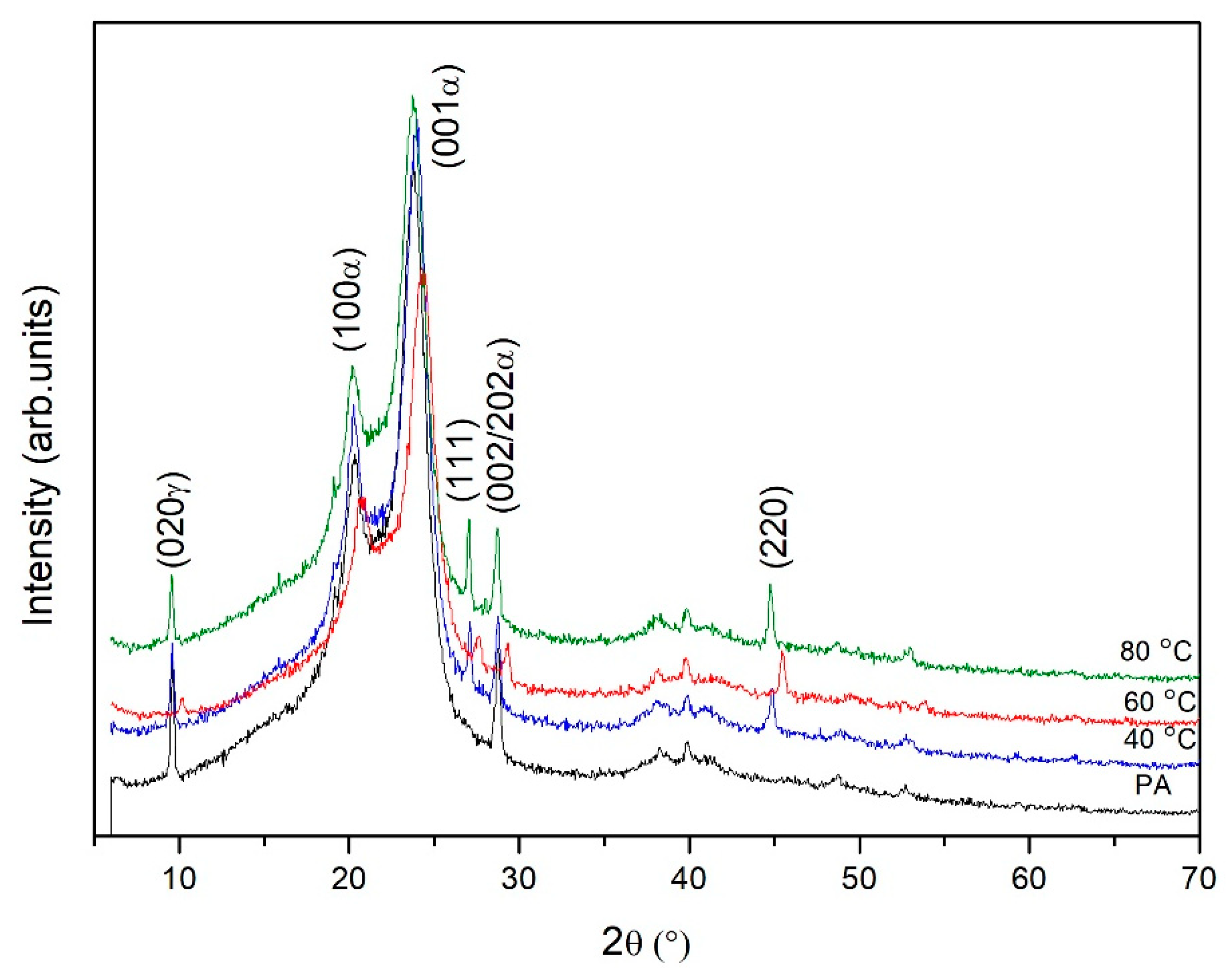
3.1. XRD Characterization of Copper Selenide Thin Films

The crystal structures and orientations of the thin copper selenide films on the PA substrate were investigated by X-ray diffraction patterns and are shown in Figure 1. The XRD results revealed that all films have a polycrystalline structure.
Semicrystalline peaks of polyamide were observed between 9° and 30° (in 2θ). These peaks, according to JCPDS 12-923, appear at 20.3° and 23.8° with the corresponding d-spacing of 4.36 and 3.74, respectively. They are attributed to the (100α) and (001α) crystal planes, respectively, showing the presence of a dominant crystalline α-phase [28,43,44]. Two reflections were also observed at around 2θ = 9.6° (020γ) and 28.8° (002/202α). XRD analysis showed that the temperature of the solutions of anionic and cationic precursors used in the experiment influenced the composition of the obtained thin films. The X-ray peaks on diffractograms are more intense when the solutions’ temperature is higher. The peaks at 28° and 45° are absent in the spectrum of pure PA and they correspond to planes (111) and (220) of a cubic phase of Cu2−xSe Berzelianite (JCPDS 6-680). It is common Cu2−xSe phase [12,15]. The experimental values of the Miller indices d, and (hkl) of PA and copper selenide thin films are given in Table 1.
Changes in the intensities and full width at half maximum (FWHM) values of these peaks were observed with the use of different temperatures of solutions. The intensities of the diffraction peak increased slightly with changing temperature of the solution temperature from 40 to 80 °C. The structural parameters for the (220) peak such as FWHM (β), grain size (D), dislocation density (δ), and strain (ε) for all films were evaluated by XRD patterns and presented in Table 2. As shown, grain size increases, while dislocation density and strain decrease with the change in the deposition temperature.
These changes can be attributed to the improvement in film crystallization and to the inductive lattice matching, which has a strong impact on structural parameters. The higher values of D, and the smaller β, δ and ε values indicate better crystallization of thin films. Regarding the values of D, β, and δ, the best results were obtained for the film made at 80 °C, suggesting that a higher temperature facilitates the crystallization of the film.

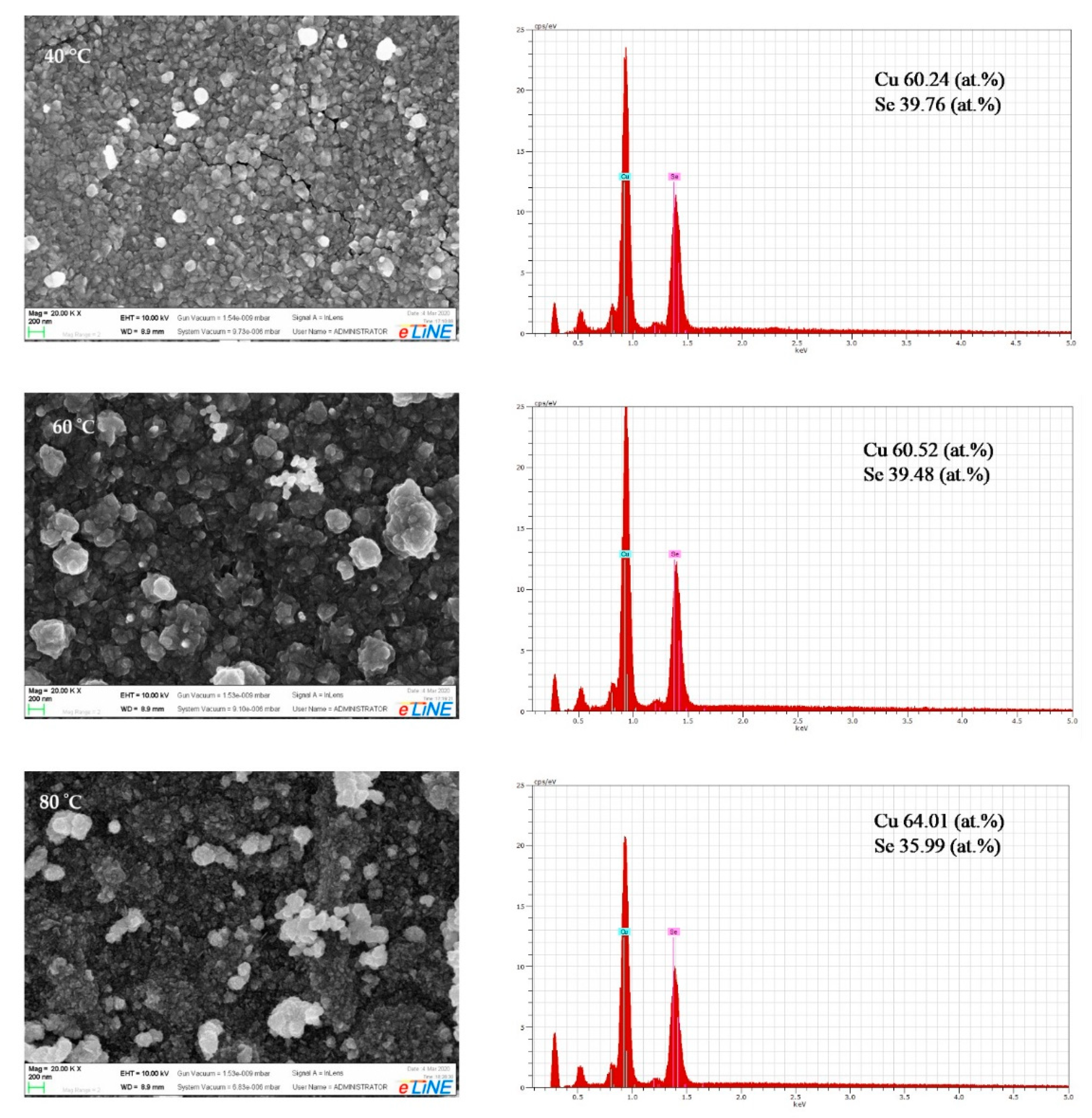
3.2. Scanning Electron Microscopy and Energy Dispersive X-ray Analysis

Scanning electron microscopy was used to evaluate the changes in surface morphology of the copper selenide layer on the PA substrate, with the changes in synthesis parameters. The SEM micrographs of the samples are presented on the left-hand side of Figure 2, with a magnification of 20,000 k. The images clearly show that the polymer is well-covered with copper selenide thin films.
Copper selenide grains grow in irregular shapes and sizes. By changing temperature, it could be seen that when the temperature increases, the copper selenide film becomes denser, coated with tightly packed spherical grains that, in turn, were combined into agglomerates of 100 nm to 1 µm. Micrographs show a compact structure composed of single types of small, densely packed microcrystals. The thin copper selenide films on surface of PA are well dispersed, relatively uniform, and consist of randomly oriented particles. Such morphological forms can produce a very rough surface with high porosity, which leads to increased catalytic activity.
The elemental analysis of the copper selenide thin films was performed using an EDX micro-analytic unit attached with scanning electron microscopy and shown on the right-hand side of Figure 2. The presence of emission lines in the investigated energy range indicates that copper selenide films were successfully deposited on the polyamide substrates and the expected elements (selenium and copper) were detected. The element analysis revealed the presence of Cu and Se with the average atomic percentages shown on the right side of Figure 2. All films show a higher atomic presence of Cu than Se, which confirms the presence of Cu2−xSe. The Cu/Se ratio measured by EDX analysis was 1.52–1.78, which is in good agreement with the XRD results.

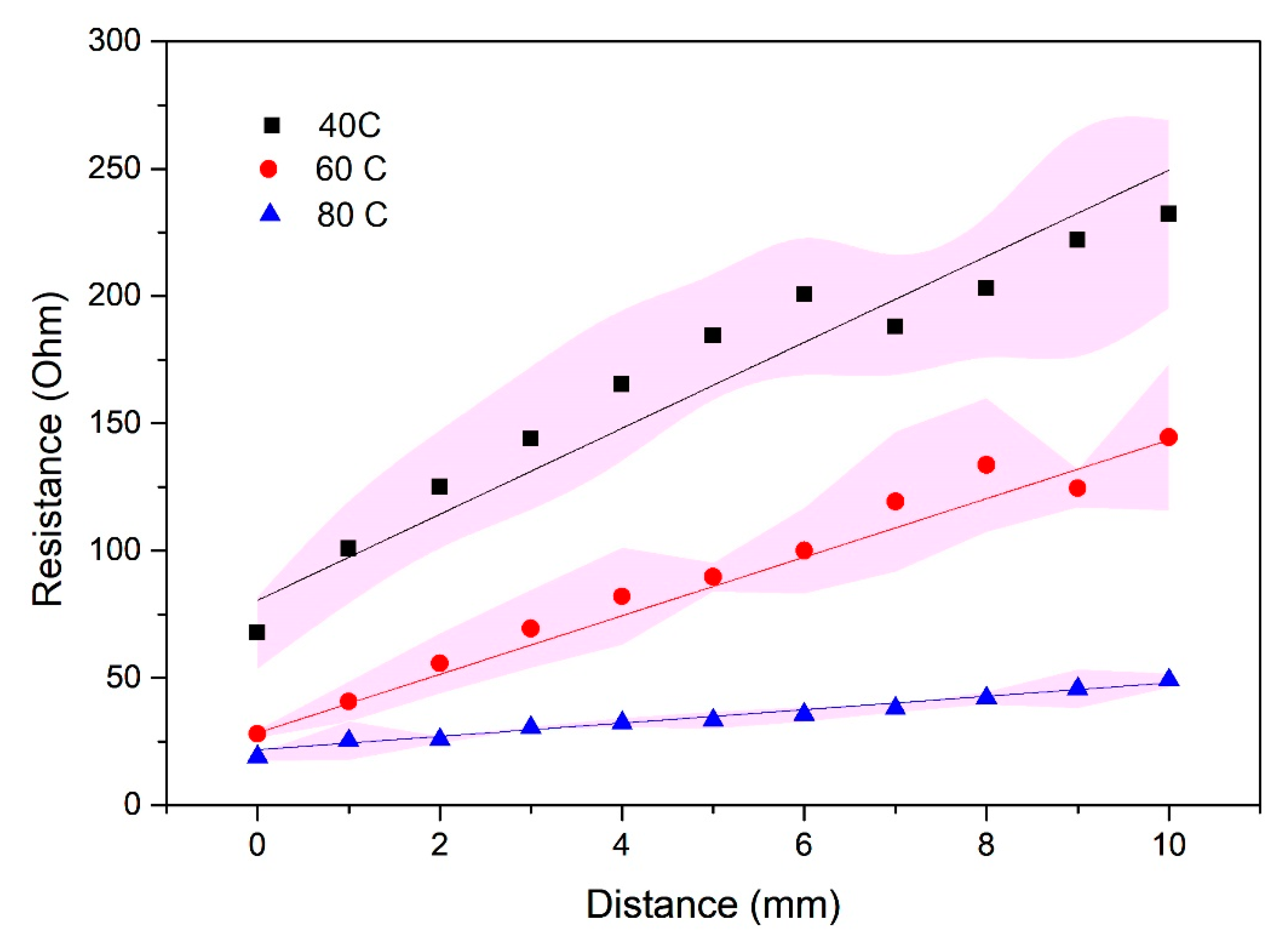
3.3. Measurements of Electrical Resistivity

The resistance of thin films of copper selenide formed on PA plotted in Figure 3 is measured from the close contact up to the 1 cm distance of electrodes, and it includes the contact resistance of the electrode contacts. On the contrary, the pure PA substrate shows no electrical conductivity—the material is a pure insulator.
At a distance of 1 cm between the electrodes, the resistances of films obtained at 40 °C, 60 °C and 80 °C are 270 Ω, 124 Ω and 49 Ω, while the values for the close contact between the electrodes were obtained to be 50 Ω, 26 Ω and 20 Ω, respectfully. The corresponding slopes are 16, 11, and 2.6, which implies that the electrical properties of the film improve with elevating the temperature. Compared to XRD results, the sample obtained at 80 °C has the best crystallinity, which is directly connected with higher conductivity (i.e., lower resistivity). As it can be seen in the graph, the error bar values are minimal for the sample obtained at 80 °C, and they increase with decreasing the temperature.

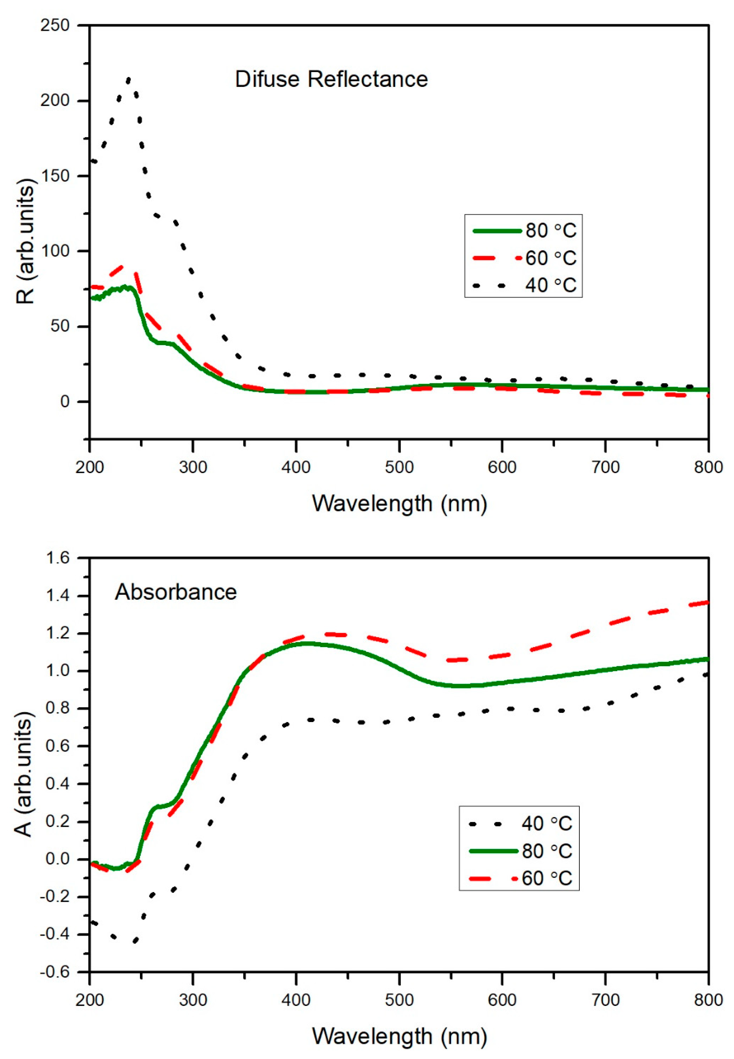
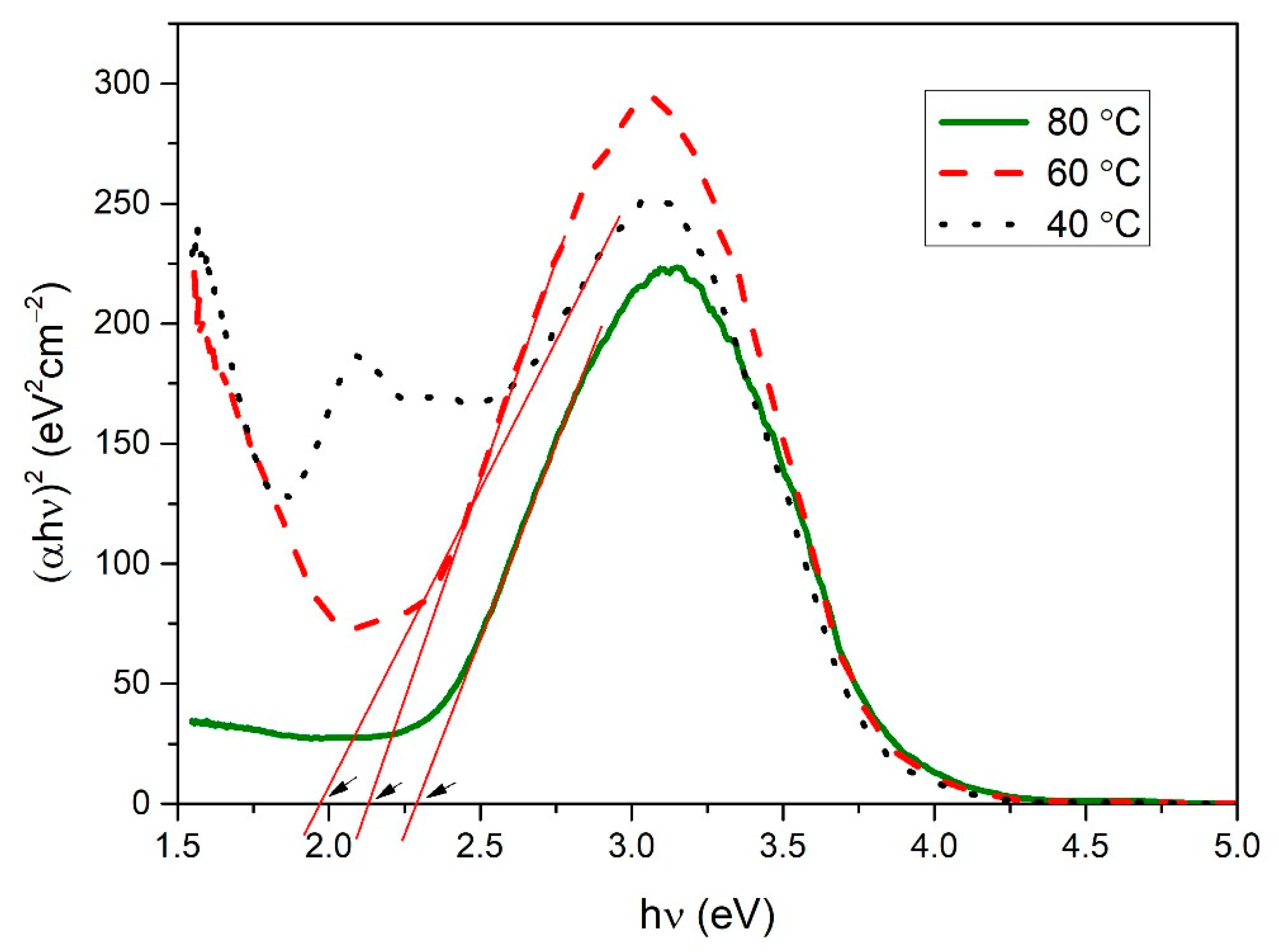
3.4. Optical Analysis of Copper Selenide Thin Films

The absorbance and diffuse reflectance spectra of thin films of copper selenide on PA in the wavelength range of 200–800 nm are presented in Figure 4. An increase in the absorbance of the copper selenide films is observed with the increased temperature of solutions, as well as the opposite effect of the reflectance.
The determination of band gaps in semiconductors is significant for obtaining basic solid-state physics.
In this study, we used the Tauc plot for the determination of the optical band gap from diffuse reflectance measurements [40,41,42]. The experimental values of energy gaps for copper selenide thin films are determined to be 2.28 eV for the sample obtained at 80 °C, 2.14 eV for the sample at 60 °C, and 1.98 eV for the sample obtained at 40 °C (Figure 5). This is in good agreement with the values of the reported data [3,5,6].
The obtained band gap values are also consistent with AFM data, according to the rule—the smaller particle size, the bigger the band gap.

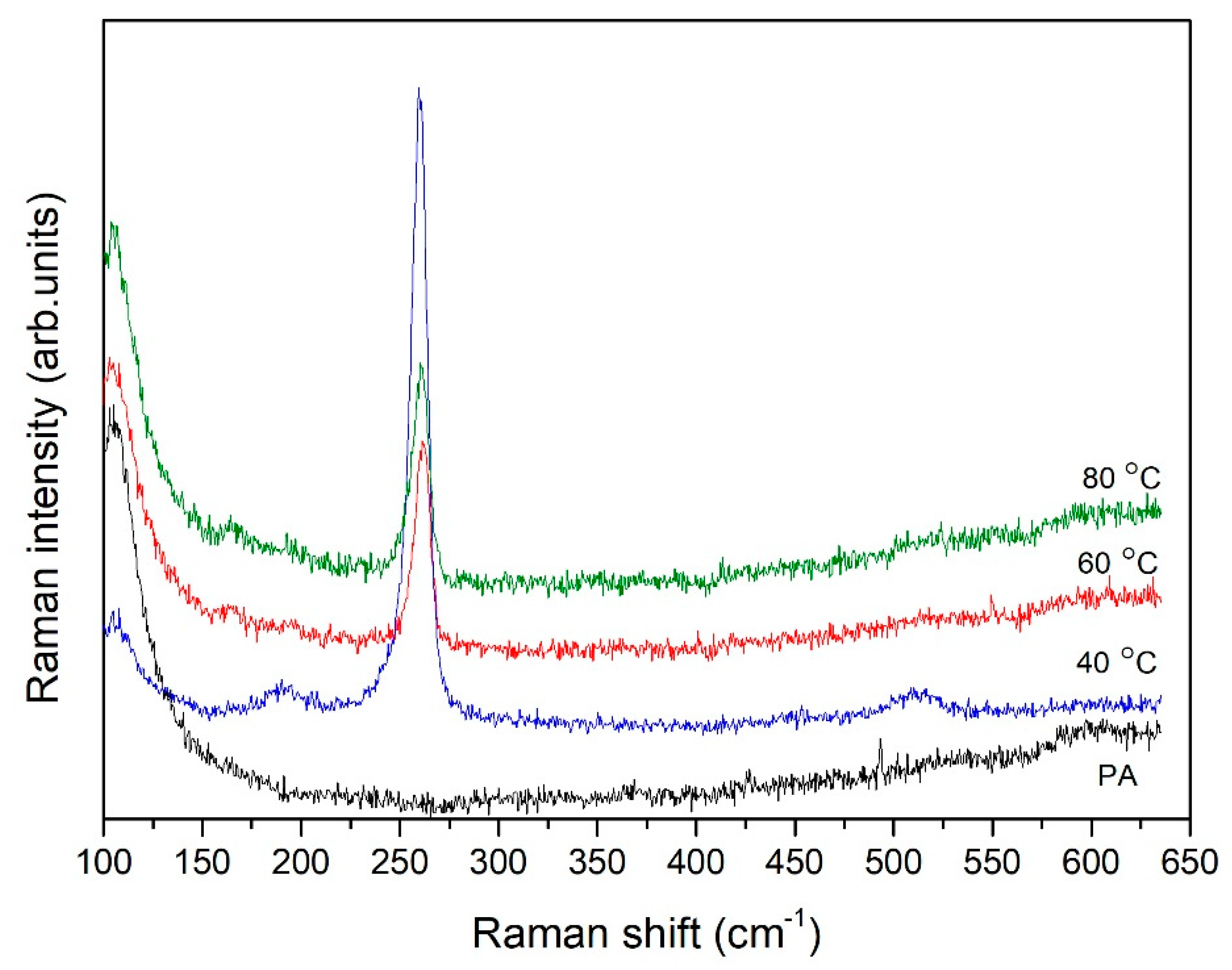
3.5. Raman Analysis of Copper Selenide Thin Films

Raman spectroscopy is a useful spectroscopic technique for detecting the vibration energy levels of compounds and for further confirming the crystal structure.
Consequently, further clarity on the crystalline phase of the copper selenide thin films was explored by Raman analysis. As shown in Figure 6, the typical Raman spectra of three copper selenide film samples (deposited at different temperatures) exhibit similar peak positions.
The only strong peak, observed at 260 cm−1, can be assigned to the Se–Se stretching vibration in Cu2−xSe and is consistent with the previous reports [11,45], while the peak at 187 cm−1 corresponds to the Cu-Se vibration [46]. The peak at 520 cm−1 is the first overtone of the intensive peak at 260 cm−1. Raman analysis confirms the composition of the copper selenide/PA films. There are no modes of elemental selenium or copper. The background at the beginning of the spectra comes from PA.

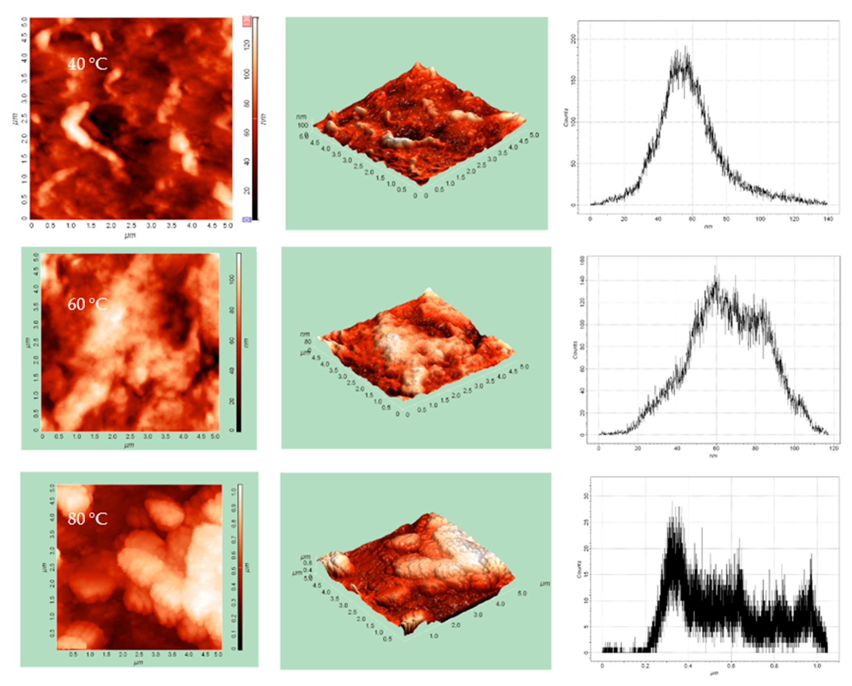
3.6. AFM Analysis of Copper Selenide Thin Films

Atomic force microscopy is a very suitable method for visualizing the surface morphology and quantitative analysis of surface roughness. 2D and 3D images, as well as histograms of 5 × 5 μm areas of copper selenide/PA films, are presented in Figure 7. The height and surface morphology of the copper selenide thin films formed on PA depend on the temperature of the solutions of anionic and cationic precursors used in the experiment: the microstructure of the thin film changes according to the deposition temperature. The surface image shows that the surface of the film is rough with particles gathered into agglomerates. The typical parameters of the quantitative analysis of AFM images are presented in Table 3. With an increase in the precursor solution temperature, the surface roughness decreases and the film becomes more compact and dense. Average roughness is ~194 nm at a precursor solution temperature of 40 °C and decreases to ~16 nm and ~13 nm in case of the temperature of 60 °C and 80 °C. As can be seen, a thin film of copper selenide deposited at 80 °C temperature solution has greater uniformity and homogeneity than other films.

4. Conclusions

Cu2−xSe thin films can be deposited on a flexible polyamide substrate by using the SILAR method, while by adjusting the temperature of precursor solutions we can affect and tune the optical, structural, and electrical properties of as obtained films. XRD analysis revealed that Cu2−xSe exists in the cubic crystal structure. The band gap energy of Cu2−xSe films was found to be in the order of 1.98–2.28 eV. Raman analysis confirmed the formation of the Cu2−xSe phase (260 cm−1) without any elemental selenium or copper phase. A thin film of copper selenide deposited at 80 °C temperature solution has greater uniformity and homogeneity than other films, the largest grain size, but with the smallest agglomerates, the largest band gap value, and the best conductivity.

Author Contributions

Conceptualization, N.P. and G.J.; methodology, N.P., G.J. and E.P.; validation, M.G., N.P. and G.J.; formal analysis, N.P., G.J. and E.P.; investigation, G.J., J.M., J.C. and U.R.; data curation, M.G., J.C., U.R. and E.G.; writing—original draft preparation, G.J. and N.P.; writing—review and editing, N.P., M.G. and E.P.; visualization, G.J. and E.U.; supervision, N.P. and M.G. All authors have read and agreed to the published version of the manuscript.

Funding

This research received no external funding.

Institutional Review Board Statement

Not applicable.

Informed Consent Statement

Not applicable.

Data Availability Statement

Not applicable.

Conflicts of Interest

The authors declare no conflict of interest.

References

  1. García, V.M.; Nair, P.K.; Nair, M.T.S. Copper Selenide Thin Films by Chemical Bath Deposition. J. Cryst. Growth 1999, 203, 113–124. [Google Scholar] [CrossRef]
  2. Tyagi, K.; Gahtori, B.; Bathula, S.; Jayasimhadri, M.; Singh, N.K.; Sharma, S.; Haranath, D.; Srivastava, A.K.; Dhar, A. Enhanced Thermoelectric Performance of Spark Plasma Sintered Copper-Deficient Nanostructured Copper Selenide. J. Phys. Chem. Solids 2015, 81, 100–105. [Google Scholar] [CrossRef]
  3. Thirumavalavan, S.; Mani, K.; Sagadevan, S. Investigation of the Structural, Optical and Electrical Properties of Copper Selenide Thin Films. Mater. Res. 2015, 18, 1000–1007. [Google Scholar] [CrossRef]
  4. Zhao, L.; Wang, X.; Yun, F.F.; Wang, J.; Cheng, Z.; Dou, S.; Wang, J.; Snyder, G.J. The Effects of Te2− and I Substitutions on the Electronic Structures, Thermoelectric Performance, and Hardness in Melt-Quenched Highly Dense Cu2−xSe. Wiley Online Libr. 2015, 1, 1400015. [Google Scholar] [CrossRef] [Green Version]
  5. Hussain, R.A.; Hussain, I. Copper Selenide Thin Films from Growth to Applications. Solid State Sci. 2020, 100, 106101. [Google Scholar] [CrossRef]
  6. Hankare, P.P.; Khomane, A.S.; Chate, P.A.; Rathod, K.C.; Garadkar, K.M. Preparation of Copper Selenide Thin Films by Simple Chemical Route at Low Temperature and Their Characterization. J. Alloy. Compd. 2009, 469, 478–482. [Google Scholar] [CrossRef]
  7. Silva, S.F.C.; Zanatta, B.S.; Rabelo, A.C.; Bottecchia, O.L.; Tozoni, J.R.; Oliveira, O.N.; Marletta, A. Flexible and Transparent Electrodes of Cu2−XSe with Charge Transport via Direct Tunneling Effect. Adv. Electron. Mater. 2021, 7, 2001189. [Google Scholar] [CrossRef]
  8. Zyoud, A.; Murtada, K.; Kwon, H.; Choi, H.J.; Kim, T.W.; Helal, M.H.S.; Faroun, M.; Bsharat, H.; Park, D.H.; Hilal, H.S. Copper Selenide Film Electrodes Prepared by Combined Electrochemical/Chemical Bath Depositions with High Photo-Electrochemical Conversion Efficiency and Stability. Solid State Sci. 2018, 75, 53–62. [Google Scholar] [CrossRef]
  9. Kalenga, M.P.; Govindraju, S.; Airo, M.; Moloto, M.J.; Sikhwivhilu, L.M.; Moloto, N. Fabrication of a Schottky Device Using CuSe Nanoparticles: Colloidal versus Microwave Digestive Synthesis. J. Nanosci. Nanotechnol. 2015, 15, 4480–4486. [Google Scholar] [CrossRef]
  10. Singh, S.C.; Li, H.; Yao, C.; Zhan, Z.; Yu, W.; Yu, Z.; Guo, C. Structural and Compositional Control in Copper Selenide Nanocrystals for Light-Induced Self-Repairable Electrodes. Nano Energy 2018, 51, 774–785. [Google Scholar] [CrossRef]
  11. Xu, J.; Yang, Q.; Kang, W.; Huang, X.; Wu, C.; Wang, L.; Luo, L.; Zhang, W.; Lee, C.S. Water Evaporation Induced Conversion of CuSe Nanoflakes to Cu2−XSe Hierarchical Columnar Superstructures for High-Performance Solar Cell Applications. Part. Part. Syst. Charact. 2015, 32, 840–847. [Google Scholar] [CrossRef]
  12. Zhou, R.; Huang, Y.; Zhou, J.; Niu, H.; Wan, L.; Li, Y.; Xu, J.; Xu, J. Copper Selenide (Cu3Se2 and Cu2−xSe) Thin Films: Electrochemical Deposition and Electrocatalytic Application in Quantum Dot-Sensitized Solar Cells. Dalton Trans. 2018, 47, 16587. [Google Scholar] [CrossRef] [PubMed]
  13. Zhang, H.; Xia, Y. Ratiometry, Wavelength, and Intensity: Triple Signal Readout for Colorimetric Sensing of Mercury Ions by Plasmonic Cu2−xSe Nanoparticles. ACS Sens. 2016, 1, 384–391. [Google Scholar] [CrossRef]
  14. Wang, Z.; Peng, F.; Wu, Y.; Yang, L.; Zhang, F.; Huang, J. Template Synthesis of Cu2−xSe Nanoboxes and Their Gas Sensing Properties. Cryst. Eng. Comm. 2012, 14, 3528–3533. [Google Scholar] [CrossRef]
  15. Astam, A.; Akaltun, Y.; Yildirim, M. Conversion of SILAR Deposited Cu3Se2 Thin Films to Cu2−XSe by Annealing. Mater. Lett. 2016, 166, 9–11. [Google Scholar] [CrossRef]
  16. Bhuse, V.M.; Hankare, P.P.; Garadkar, K.M.; Khomane, A.S. A Simple, Convenient, Low Temperature Route to Grow Polycrystalline Copper Selenide Thin Films. Mater. Chem. Phys. 2003, 80, 82–88. [Google Scholar] [CrossRef]
  17. Li, X.; Li, P.; Wu, Z.; Luo, D.; Yu, H.-Y.; Lu, Z.-H. Review and Perspective of Materials for Flexible Solar Cells. Mater. Rep. Energy 2021, 1, 100001. [Google Scholar] [CrossRef]
  18. Yoon, H.; Kang, S.M.; Lee, J.K.; Choi, M. Hysteresis-Free Low-Temperature-Processed Planar Perovskite Solar Cells with 19.1% Efficiency. Energy Environ. Sci. 2016, 9, 2262–2266. [Google Scholar] [CrossRef]
  19. Aernouts, T.; Vanlaeke, P.; Geens, W.; Poortmans, J.; Heremans, P.; Borghs, S.; Mertens, R.; Andriessen, R.; Leenders, L. Printable Anodes for Flexible Organic Solar Cell Modules. Thin Solid Film. 2004, 451–452, 22–25. [Google Scholar] [CrossRef]
  20. Fonrodona, M.; Escarré, J.; Villar, F.; Soler, D.; Asensi, J.M.; Bertomeu, J.; Andreu, J. PEN as Substrate for New Solar Cell Technologies. Sol. Energy Mater. Sol. Cells 2005, 89, 37–47. [Google Scholar] [CrossRef] [Green Version]
  21. Chen, H.; Gu, Z.G.; Zhang, J. Chiral-Induced Ultrathin Covalent Organic Frameworks Nanosheets with Tunable Circularly Polarized Luminescence. J. Am. Chem. Soc. 2022, 144, 7245–7252. [Google Scholar] [CrossRef] [PubMed]
  22. Hassan, M.; Abbas, G.; Li, N.; Afzal, A.; Haider, Z.; Ahmed, S.; Xu, X.; Pan, C.; Peng, Z. Significance of Flexible Substrates for Wearable and Implantable Devices: Recent Advances and Perspectives. Adv. Mater. Technol. 2022, 7, 2100773. [Google Scholar] [CrossRef]
  23. Wang, K.; Cheng, S.; Hu, Q.; Yu, F.; Cheng, Y.; Huang, K.; Yuan, H.; Jiang, J.; Li, W.; Li, J.; et al. Vertical Graphene-Coated Cu Wire for Enhanced Tolerance to High Current Density in Power Transmission. Nano Res. 2021, 14, 1–7. [Google Scholar] [CrossRef]
  24. Chen, Y.; Gao, C.; Yang, T.; Li, W.; Xu, H.; Sun, Z.; Chen, Y.; Gao, C.; Yang, T.; Li, W.; et al. Research Advances of Ferroelectric Semiconductors of 2D Hybrid Perovskites toward Photoelectronic Applications. Chin. J. Struct. Chem. 2022, 41, 2204001–2204011. [Google Scholar] [CrossRef]
  25. Chang, H.B.; Liu, J.B.; Dong, Z.; Wang, D.D.; Xin, Y.; Jiang, Z.L.; Tang, S.S. Enhancement of Photocatalytic Degradation of Polyvinyl Chloride Plastic with Fe2O3 Modified AgNbO3 Photocatalyst under Visible-Light Irradiation. Jiegou Huaxue 2021, 40, 1595–1603. [Google Scholar] [CrossRef]
  26. Vikulov, S.; di Stasio, F.; Ceseracciu, L.; Saldanha, P.L.; Scarpellini, A.; Dang, Z.; Krahne, R.; Manna, L.; Lesnyak, V. Fully Solution-Processed Conductive Films Based on Colloidal Copper Selenide Nanosheets for Flexible Electronics. Adv. Funct. Mater. 2016, 26, 3670–3677. [Google Scholar] [CrossRef] [Green Version]
  27. Qu, C.; Hu, J.; Liu, X.; Li, Z.; Ding, Y. Morphology and Mechanical Properties of Polyimide Films: The Effects of UV Irradiation on Microscale Surface. Materials 2017, 10, 1329. [Google Scholar] [CrossRef] [Green Version]
  28. Parodi, E.; Peters, G.W.M.; Govaert, L.E. Structure-Properties Relations for Polyamide 6, Part 1: Influence of the Thermal History during Compression Moulding on Deformation and Failure Kinetics. Polymers 2018, 10, 710. [Google Scholar] [CrossRef] [Green Version]
  29. Janickis, V.; Petrašauskiene, N.; Žalenkiene, S.; Morkvenaite-Vilkoňciene, I.; Ramanavǐcius, A. Morphology of CdSe-Based Coatings Formed on Polyamide Substrate. J. Nanosci. Nanotechnol. 2018, 18, 604–613. [Google Scholar] [CrossRef]
  30. Ivanauskas, R.; Milasiene, D. Fabrication of Polyamide-Ag2Se Composite Films with Controllable Properties by an Adsorption–Diffusion Method. J. Phys. Chem. Solids 2020, 145, 109533. [Google Scholar] [CrossRef]
  31. Lakshmi, M.; Bindu, K.; Bini, S.; Vijayakumar, K.P.; Sudha Kartha, C.; Abe, T.; Kashiwaba, Y. Chemical Bath Deposition of Different Phases of Copper Selenide Thin Films by Controlling Bath Parameters. Thin Solid Film. 2000, 370, 89–95. [Google Scholar] [CrossRef]
  32. Xu, S.; Wang, H.; Zhu, J.J.; Chen, H.Y. Sonochemical Synthesis of Copper Selenides Nanocrystals with Different Phases. J. Cryst. Growth 2002, 234, 263–266. [Google Scholar] [CrossRef]
  33. Li, Y.D.; Fan, P.; Zheng, Z.H.; Luo, J.T.; Liang, G.X.; Guo, S.Z. The Influence of Heat Treatments on the Thermoelectric Properties of Copper Selenide Thin Films Prepared by Ion Beam Sputtering Deposition. J. Alloy. Compd. 2016, 658, 880–884. [Google Scholar] [CrossRef]
  34. Güzeldir, B.; Sağlam, M. Using Different Chemical Methods for Deposition of Copper Selenide Thin Films and Comparison of Their Characterization. Spectrochim. Acta Part A Mol. Biomol. Spectrosc. 2015, 150, 111–119. [Google Scholar] [CrossRef]
  35. Pathan, H.M.; Lokhande, C.D. Deposition of Metal Chalcogenide Thin Films by Successive Ionic Layer Adsorption and Reaction (SILAR) Method. Bull. Mater. Sci. 2004, 27, 85–111. [Google Scholar] [CrossRef]
  36. Bragg, W.H.; Bragg Apr, W.L.; H Bragg, B.W.; Professor of Physics, C. The Reflection of X-Rays by Crystals. Proc. R. Soc. London. Ser. A Contain. Pap. A Math. Phys. Character 1913, 88, 428–438. [Google Scholar] [CrossRef]
  37. Patterson, A.L. The Scherrer Formula for X-Ray Particle Size Determination. Phys. Rev. 1939, 56, 978. [Google Scholar] [CrossRef]
  38. Nath, D.; Singh, F.; Das, R. X-Ray Diffraction Analysis by Williamson-Hall, Halder-Wagner and Size-Strain Plot Methods of CdSe Nanoparticles—A Comparative Study. Mater. Chem. Phys. 2020, 239, 122021. [Google Scholar] [CrossRef]
  39. Ashraf, M.; Akhtar, S.M.J.; Khan, A.F.; Ali, Z.; Qayyum, A. Effect of Annealing on Structural and Optoelectronic Properties of Nanostructured ZnSe Thin Films. J. Alloy. Compd. 2011, 509, 2414–2419. [Google Scholar] [CrossRef]
  40. Tauc, J.; Grigorovici, R.; Vancu, A. Optical Properties and Electronic Structure of Amorphous Germanium. Phys. Status Solidi (B) 1966, 15, 627–637. [Google Scholar] [CrossRef]
  41. Makuła, P.; Pacia, M.; Macyk, W. How To Correctly Determine the Band Gap Energy of Modified Semiconductor Photocatalysts Based on UV-Vis Spectra. J. Phys. Chem. Lett. 2018, 9, 6814–6817. [Google Scholar] [CrossRef] [PubMed] [Green Version]
  42. Petrović, M.; Gilić, M.; Ćirković, J.; Romčević, M.; Romčević, N.; Trajić, J.; Yahia, I. Optical Properties of CuSe Thin Films—Band Gap Determination. Sci. Sinter. 2017, 49, 167–174. [Google Scholar] [CrossRef] [Green Version]
  43. Banerjee, S.S.; Janke, A.; Gohs, U.; Heinrich, G. Electron-Induced Reactive Processing of Polyamide 6/Polypropylene Blends: Morphology and Properties. Eur. Polym. J. 2018, 98, 295–301. [Google Scholar] [CrossRef]
  44. Zhao, X.Y.; Zhang, B.Z. The Effects of Annealing (Solid and Melt) on the Time Evolution of the Polymorphic Structure of Polyamide 6. J. Appl. Polym. Sci. 2010, 115, 1688–1694. [Google Scholar] [CrossRef]
  45. Minceva-Sukarova, B.; Najdoski, M.; Grozdanov, I.; Chunnilall, C.J. Raman Spectra of Thin Solid Films of Some Metal Sulfides. J. Mol. Struct. 1997, 410–411, 267–270. [Google Scholar] [CrossRef]
  46. Malavekar, D.B.; Bulakhe, R.N.; Kale, S.B.; Patil, U.M.; In, I.; Lokhande, C.D. Synthesis of Layered Copper Selenide on Reduced Graphene Oxide Sheets via SILAR Method for Flexible Asymmetric Solid-State Supercapacitor. J. Alloy. Compd. 2021, 869, 159198. [Google Scholar] [CrossRef]
Figure 1. XRD patterns of the initial PA and copper selenide thin films.
Chemosensors 10 00313 g001
Figure 2. SEM micrographs and EDX spectra of copper selenide/PA thin films.
Chemosensors 10 00313 g002
Figure 3. Resistance vs. distance graph for copper selenide films on PA. The results are the averaged values of 4 measurements, and error bars are indicated as the pink area.
Chemosensors 10 00313 g003
Figure 4. Diffuse reflectance and absorbance spectra of copper selenide/PA thin films.
Chemosensors 10 00313 g004
Figure 5. Plots of (αhν)2 versus hν for copper selenide/PA thin films.
Chemosensors 10 00313 g005
Figure 6. Raman spectra of the copper selenide/PA thin films.
Chemosensors 10 00313 g006
Figure 7. 2D and 3D AFM images and histograms of copper selenide/PA films.
Chemosensors 10 00313 g007
Table 1. Values of the Miller indices d, 2θ and (hkl) of PA and copper selenide thin films.
Miller Indices (hkl) Temperature
PA40 °C60 °C80 °C
(2θ)d (Å)(2θ)d (Å)(2θ)d (Å)(2θ)d (Å)
PA(020γ)9.69.219.659.1610.28.679.69.21
(100α)20.354.3620.34.3720.954.2420.254.38
(001α)23.83.74243.7024.33.6623.753.74
Cu2−xSe(111)27.153.2827.73.2227.13.28
PA(002/202α)28.753.1028.83.1029.43.0428.753.10
Cu2−xSe(220)44.952.0245.51.9944.82.02
Table 2. Grain size (D), dislocation density (δ), strain (ε) and full width at half maximum (FWHM, β) values of copper selenide thin films.
Temperature (°)β (°)D (nm)δ·10−3 (nm−2)ε·10−3 (nm−2)
40 °C44.951.306.6122.8913.72
60 °C45.50.6014.334.866.25
80 °C44.80.5415.814.005.76
Table 3. Surface roughness parameters of copper selenide thin films.
ParametersTemperature
40 °C60 °C80 °C
Maximum height of peaks, hmax, nm1048.41117.32123.16
Average height, hmean, nm565.5765.6449.99
Average Roughness, Ra, nm194.6216.2413.32
RMS Roughness, Rq, nm227.7619.9017.21
Surface skewness, Rsk 0.42−0.130.58
Publisher’s Note: MDPI stays neutral with regard to jurisdictional claims in published maps and institutional affiliations.

