Article

Proving Surface Plasmons in Graphene Nanoribbons Organized as 2D Periodic Arrays and Potential Applications in Biosensors

1
Department of Chemistry, Universidad Técnica Particular de Loja, Loja 110160, Ecuador
2
Faculty of Mechanical Engineering, Escuela Superior Politécnica de Chimborazo (ESPOCH), Riobamba 060155, Ecuador
3
Facultad de Ciencias, Escuela Superior Politécnica de Chimborazo (ESPOCH), Riobamba 060155, Ecuador
4
Joint Laboratory of Optics of Palacký University and Institute of Physics of CAS, Faculty of Science, Palacký University, 17 listopadu 12, 771 46 Olomouc, Czech Republic
5
Surface Nanoscience Group, Department of Physics, University of Calabria, Via P. Bucci, Cubo 33C, I-87036 Rende, Italy
6
Dirección de Investigación y Vinculación, Universidad Estatal de Bolívar, Av. Ernesto Ché Guevara y Gabriel Secaira, Guaranda 020150, Ecuador
7
UNICARIBE Research Center, University of Calabria, I-87036 Rende, Italy
*
Author to whom correspondence should be addressed.
Chemosensors 2022, 10(12), 514; https://doi.org/10.3390/chemosensors10120514
Submission received: 24 October 2022 / Revised: 17 November 2022 / Accepted: 30 November 2022 / Published: 3 December 2022

Abstract

:
Surface-plasmon-based biosensors have become excellent platforms for detecting biomolecular interactions. While there are several methods to exciting surface plasmons, the major challenge is improving their sensitivity. In relation to this, graphene-based nanomaterials have been theoretically and experimentally proven to increase the sensitivity of surface plasmons. Notably, graphene nanoribbons display more versatile electronic and optical properties due to their controllable bandgaps in comparison to those of zero-gap graphene. In this work, we use a semi-analytical approach to investigate the plasmonic character of two-dimensional graphene nanoribbon arrays, considering free-standing models, i.e., models in which contact with the supporting substrate does not affect their electronic properties. Our findings provide evidence that the plasmon frequency and plasmon dispersion are highly sensitive to geometrical factors or the experimental setup within the terahertz regime. More importantly, possible applications in the molecular detection of lactose, α-thrombin, chlorpyrifos-methyl, glucose, and malaria are discussed. These predictions can be used in future experiments, which, according to what is reported here, can be correctly fitted to the input parameters of possible biosensors based on graphene nanoribbon arrays.

1. Introduction

Plasmons are coherent and collective oscillations of valence electrons on the surface of conducting or semiconducting materials as well as topological insulators (e.g., gold, silver, Cu2-XS, and Bi2Te3) [1]. Interestingly, these collective oscillations are characterized by a strong interaction with light and a small spatial extension compared with the wavelength of light [2]. A point to highlight is the fact that the control over the spectral and spatial properties of these oscillations has attracted a huge amount of attention due to their applications in ultrasensitive detection down to the single-molecule level [3], enhanced photovoltaics [4], cancer therapy [5], and nonlinear optics [6], among others. Mostly, surface plasmons in metals (solid specimens) show a low level of control of the plasmon frequency and a small plasmon propagation length which can be solved by using metal nanoparticles [7]. In this context, novel nanomaterials have been investigated; for instance, graphene (a two-dimensional (2D) honeycomb carbon material [8,9,10]) has emerged as a powerful plasmonic nanomaterial [11,12,13], increasing the number of potential applications, mainly, in surface plasmon resonance biosensors (e.g., graphene-based prism-coupled biosensors [14], graphene-based fiber-coupled biosensors [15], graphene-based grating-coupled biosensors [16], graphene-based nanoparticle-coupled biosensors [17], graphene-based plasmon-coupled emission biosensors [18], and surface-enhanced Raman-scattering biosensors [19]).
Surface plasmons in graphene offer several advantages over metals; for instance, (i) these collective oscillations are found in the terahertz-to-midinfrared frequency range, and (ii) the charge carrier concentration in graphene can be tuned by doping, which enables the electrostatic control of its electronic and optical properties [20]. Specifically, two plasmon excitations have been observed in graphene at low energies ( < 1 eV): a 2D (surface) plasmon and an acoustic plasmon [21,22]. It is worth noting that plasmon-enhanced infrared optical absorption based on 2D materials such as graphene is considered a promising spectroscopic technique for detecting vibrational modes in biopolymers, such as proteins, nucleic acids, and synthetic polymers [23,24].
An extra tunability of the 2D surface plasmon by direct optical excitation has been observed in graphene nanoribbons (GNRs). GNRs are quasi-one-dimensional structures with two different possible chiral-edge geometries at the atomistic scale (i.e., ultra-narrow systems), namely zigzag or armchair [25,26]. Nevertheless, the chiral-edge effect disappears with increases in the ribbon width. GNRs have different electronic and optical properties than pristine graphene; for instance, graphene is a gapless material, while all GNRs are semiconducting materials with bandgaps from few meV to eV [27].
Plasmons in wide GNRs have been experimentally measured, demonstrating the existence of a 2D surface plasmon and a new edge plasmon [28]. The latter arises as an effect of the charge carrier confinement due to the dimensionality change from 2D to 1D and the boundary conditions. From the technological point of view, the tunability of the 2D surface plasmon is expected to be predominant over the edge plasmon [29,30]. In order to minimize electron scattering and obtain the best plasmonic properties, GNRs organized as 2D periodic arrays [28,29] have been proposed as excellent platforms for plasmonic applications. Such ribbon systems have been experimentally realized by Fei et al., with ribbon widths of 155, 270, 380, and 480 nm [28]. In the literature to date, there have been no theoretical reports on the plasmon behavior in these 2D GNR arrays. Previous theoretical studies have explored plasmons in ultra-narrow GNR arrays ( < 2 nm), mainly by time-dependent density functional theory (TDDFT) within the random phase approximation (RPA) [29]. Nevertheless, this atomistic approach cannot be used to handle the vast number of atoms involved in wide GNRs ( > 100 nm wide).
Recently, we have described a modeling approach based on a semi-analytical model [31,32,33], which with the accurate estimation of the charge carrier velocity of graphene can be used to scrutinize the electronic and plasmonic properties of narrow and wide GNR arrays. To our knowledge, this semi-analytical model has not been adapted to prove the plasmon frequency dispersion and plasmon excitation lifetime in 2D GNR arrays of widths such as those reported in Ref. [28]. Here, such a study is reported with a quasi-freestanding approach, for instance, suspended GNR systems onto the surface of honeycomb boron nitride. Particularly, we demonstrate that the plasmonic properties in wide GNRs are highly sensitive to the ribbon width change or the experimental setup. Although experimental confirmation is needed, our predictions are expected to be of immediate help in the design of future biosensors based on 2D GNR arrays.

2. Theoretical Framework

Even though we do not propose a biosensor as such, this work aims to demonstrate the sensitivity and tunability of the surface plasmons in 2D GNR arrays that can be tailored into more complex biosensor structures for a specific demand. This fact is discussed in detail in Section 4, considering possible applications in the molecular sensing of lactose, α-thrombin, chlorpyrifos-methyl, glucose, and malaria.
With this in mind, we briefly proceed to describe the theoretical framework of the semi-analytical model, which is divided into two parts: (i) numerical computations based on density functional theory (DFT) to calculate the charge carrier velocity of graphene; and (ii) analytical expressions to obtain the electronic and plasmonic features of wide 2D GNR arrays (Figure 1a). The complete theoretical description is given in Ref. [33] (and references inside) and the step-by-step approach to estimate the charge carrier velocity (Fermi velocity) of graphene is given in Ref. [31].

2.1. Semi-Analytical Model

Popov et al. [33] asserts that owing to the quasi-one-dimensional confinement of the charge carriers in GNRs, several sub-bands (En) with a bandgap (Δ) can be observed, in which the (electron/hole) band dispersion can be described as [34,35]:
E n = ± Δ 2 n 2 + 2 p 2 m * Δ
where n is the sub-band index ( n = 1 ,   2 ,   3 ,   ), p is the parallel momentum along the GNR direction, and m * is the effective electron mass. The bandgap can be estimated as follows:
Δ = 2   π   v F   w
where vF is the charge carrier velocity, w is the ribbon width, and is the reduced Planck constant. Now, the effective electron mass can be calculated by:
m * = Δ 2   v F 2
Notably, for ultra-narrow GNRs, Equation (1) displays a parabolic band structure and bandgap opening around the Γ point (Figure 1b), and this band dispersion changes to a linear behavior, with Δ 0 , with increases in the ribbon width, w (Figure 1c), similarly to the graphene band dispersion around the Κ point (Figure 2a). Hence, wide GNRs organized as 2D periodic arrays are expected to show electronic and optical properties similar to those of graphene.
It is worth noting that the estimated values of the bandgap (Equation (2)) and effective mass (Equation (3)) depend substantially on the input values of the ribbon width (i.e., m Δ * ) and the charge carrier velocity, which are reported in Tables S2 and S3.
From the point of view of plasmonics, the plasmon wavelength is expected to follow the sample length instead of the vacuum distance between the contiguous ribbons or the ribbon width, which allows us to conclude that GNR arrays can be taken as regular 2D planes (Figure S1) in which the charge carrier velocity of graphene is the critical free parameter that must be estimated (discussed below) to be introduced in the present modeling approach. Hence, with the suitable v F value, the plasmon dispersion relation can be calculated by following the strategy of Ref. [33]:
ω = Re [ 2   π   e 2   N 2 D ϵ   m * q cos   2 θ v 2 4 i v 2 ]
where e represents the electron charge, N 2 D represents the 2D electron density, ϵ represents the dielectric constant, q represents the reciprocal wave vector, θ represents the angle created along the plasmon wave vector and GNR direction, and v represents the electron relaxation rate. We point out that the real part of Equation (4) is taken to obtain the plasmon frequency dispersion.
To acquire the plasmon spectrum (i.e., plasmon excitation lifetime) for selected q values of the systems under study, a conventional Lorentzian line shape function (L) set to a maximum value of 1 can be used as follows:
L = 1 1 + 4 ( ω ω o ) W 2
where ωo is the transition frequency/energy at the specific q value (peak position) (Tables S4, S6, S8, and S10), ω is the frequency/energy range of interest, and the capital W is the full width at half maximum (FWHM). The latter was fixed to the value of 0.5 for all plasmon spectra.
It is important to note that the plasmon response is not expected to be a simple Lorentzian peak; however, we use this approach to clearly show the controllability and tunability of surface plasmons in 2D GNR arrays. Furthermore, the maximum of the plasmon peak could be delayed as an effect of core-electron excitations [36], which is not strictly considered in the proposed model. Delayed maxima have been observed in metals, such as Nb, Mo, and Ag, suggesting that this effect might be predominant in supported (non-freestanding) 2D GNR arrays.

2.2. Estimation of the Charge Carrier Velocity

The Fermi velocity of charge carriers in graphene was estimated by DFT computations at the level of the local density approximation (LDA) [37]. To do this, the following input parameters were fixed: a cut-off energy of ~680 eV, an out-of-plane distance of 15 Å to cancel out the unphysical interactions along the z -direction between replicas, a C-C bond length of 1.420 Å with a lattice constant of 2.460 Å, and a dense Monkhorst-Pack grid of 720 × 720 × 1. For details, see Ref. [31].
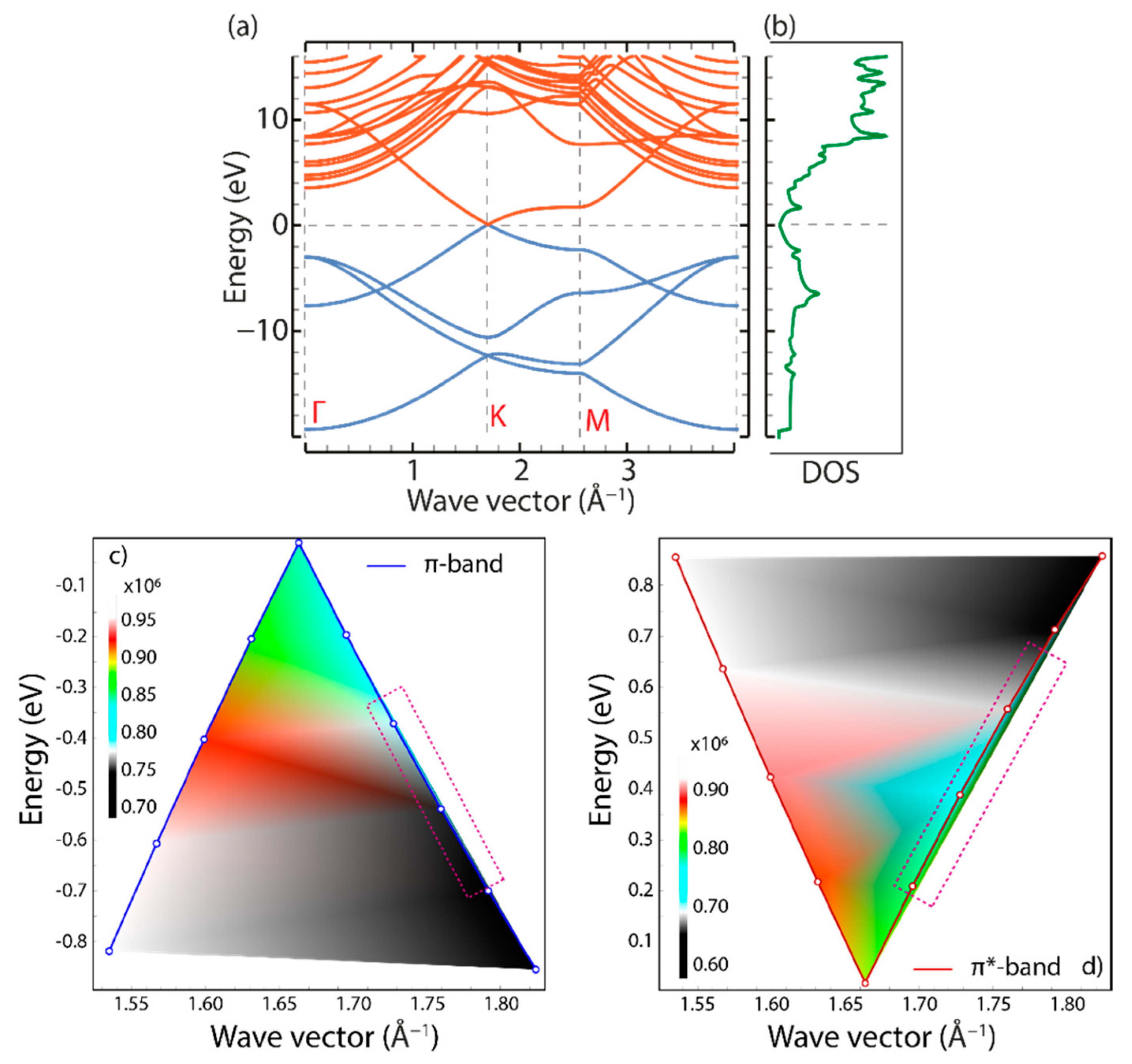
Figure 2 shows the DFT-LDA band structure (Figure 2a) and density of states (DOS) (Figure 2b) of graphene from −20 to 15 eV. Special attention should be paid from −1 to 1 eV (Figure S2a), in which the graphene band structure shows a linear electron dispersion around the K point, and as a consequence, the Dirac cone approximation can be applied. While the Fermi velocity also follows a linear behavior in the same energy-momentum range (Figure S2b, Table S1), a closer view demonstrates that the valence band ( π , blue line, Figure 2c) and conduction band ( π * , red line, Figure 2d) deviate slightly from the linear behavior of the charge carrier velocity (see rectangular dashed regions), suggesting that the semi-analytical model, which is based on the Dirac cone approximation, is valid from −0.3 to 0.2 eV, i.e., about 50 THz.
As stated, the charge carrier velocity ( v F ) of graphene was calculated in [31], whose average value was found to be v F = 0.829 × 10 6 m s−1, which is the average charge carrier velocity between the conduction ( π * ) band and valence ( π ) band.

3. Results and Discussions

3.1. Electronic Properties

In Figure 3, we show the bandgap (Δ) calculated by Equation (2) (using two different charge carrier velocities: v F = 0.829 × 10 6 m s−1 [31] (blue markers) and v F = 1.0 × 10 6 m s−1 [33] (orange markers), for the experimentally realized GNRs (155, 270, 380, 480 nm wide [28]).
As observed, regardless of the charge carrier velocity, the bandgap decreases as the ribbon width increases as expected. Nevertheless, it is important to note that the electronic properties can be over- or underestimated and therefore also the optical properties of the systems under study.
Particularly, the bandgap values of the experimental GNRs are of the order of a few meV (Tables S2 and S3); however, these numerical results differ by about 20%, suggesting a similar result for the plasmon properties. With this in mind, in the remainder of the article, we focus on the electronic and plasmonic properties of GNR arrays using the previously estimated Fermi velocity of v F = 0.829 × 10 6 m s−1, which in fact is in good agreement with previous measures [38].
GNRs 155, 270, 380, and 480 nm wide are characterized by very small bandgaps in the order of a few meV (Table S2): w 155 = 22.12 meV, w 270 = 12.70 meV, w 380 = 9.02 meV, and w 480 = 7.14 meV. The blue and orange curves predict the bandgap for GNRs from 100 to 500 nm wide. The estimated effective electron masses are in good agreement with those previously reported [35,39]. To emphasize, an ab initio treatment of these wide nanoribbons is impractical due to the vast number of atoms, demonstrating the advantage of the semi-analytical model.
In Figure 4, we show the band structure and DOS of the GNR systems of interest. The band structure is calculated by Equation (1) with the corresponding bandgap values and effective electron masses reported in Table S2 and considering a sub-band index of n = 9 (nine valence sub-bands (blue curves) and nine conduction sub-bands (black curves)). The DOS is calculated from the energy-momentum data list by using a conventional histogram with equal bin widths. Note that the band structure of the GNRs is illustrated assuming the same effective electron mass ( m * ) for all bands; however, the plasmonic properties of these are restricted to the two ( π ,   π * ) bands at the Fermi level in which the charge carrier velocity of graphene is calculated (Section 2.2).
From Figure 4, two important facts can be observed: (i) there is a direct bandgap at the Γ point; and (ii) there are several sub-bands within ±30 meV created by increasing the ribbon width, originating from strong peaks in the DOS around the zero-energy region (Fermi level, dashed black line), unlike graphene whose linear band dispersion yields a vanishing DOS at the Fermi level (Figure 2b).
As is evident, the band structure and DOS of GNRs differ from those of graphene (Figure 2a,b) regardless of ribbon width since 1D sub-bands and the bandgap opening arise due to the charge carrier confinement. Then, all GNRs are predicted to be semiconducting materials with the π (highest occupied) sub-band and π *   (lowest unoccupied) sub-band having parabolic-like band dispersions around a small gap at the Γ point (e.g., see Figure 1b).

3.2. The Effect of Ribbon Width on the Plasmonic Properties

As stated, previous works on 2D GNR arrays have demonstrated the existence of two plasmon excitations: the surface plasmon and the edge plasmon [28,29]. In addition, Yan H et al. [40] have proved the coupling between plasmon resonances in graphene micro-rings, which could also be expected for 2D GNR arrays. However, Fei Z. et al. [28] confirmed well-defined and well-separated plasmons resonances, particularly, for GNRs wider than 200 nm. Additionally, Vacacela Gome et al. [29] have demonstrated that the coupling between the surface and edge plasmon resonances is a direct effect of doping, i.e., for larger doping values, N 2 D ~ 4.0 × 10 12 cm−2 ( ~ 0.3 eV), the coupling and hybridization begin to appear. With this in mind, the proposed model here can reasonably be used for future experiments. On the other hand, from point of view of biosensors, the surface plasmon is the most interesting because its plasmon frequency relation and plasmon response can be controlled by gating or doping working on the THz scale, which in turn, is the most interesting regime of the plasmonic applications of graphene-based biosensors [41].
Before discussing the plasmonic properties of the freestanding systems in detail, it is important to note that it has been shown that the charge carrier velocity in graphene can be modulated by changing the supporting substrate [38], which should indeed substantially affect the electronic and plasmonic properties of 2D GNR arrays. The latter is confirmed in Figure S3. These outcomes require detailed and extensive work.
Figure 5 shows the plasmon frequency dispersion of the experimentally realized GNRs [28] organized as periodic 2D arrays (Figure S1) with ribbon widths ranging from 155 to 480 nm. Based on the experimental setup reported in Ref. [39], the parameters of N 2 D = 1.0 × 10 12 cm−2, ν = 1.0 × 10 13 s−1, and θ = 0 are fixed.
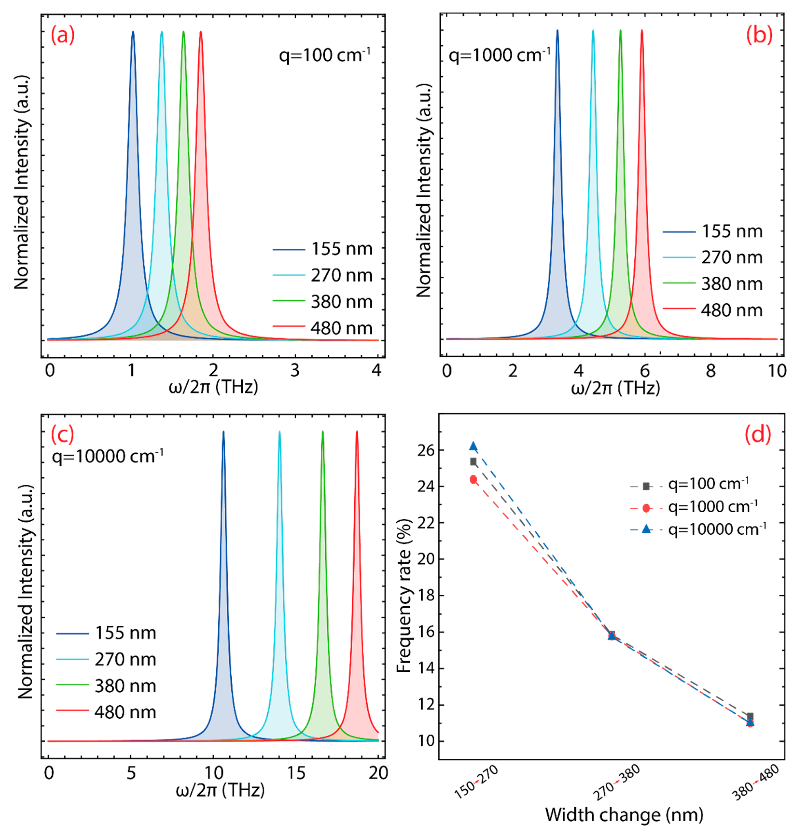
In Figure 5, The plasmon frequency trend follows a q -like dispersion regardless of the ribbon width. Indeed, this plasmon trend has been observed in well-defined 2D materials, confirming the viability of the semi-analytical model to analyze the plasmonic properties of 2D GNR arrays. Another important result is the fact that increasing the ribbon width increases the plasmon frequency, for instance, from 10.63 THz ( w = 155 nm, blue line) to 18.71 THz ( w = 480 nm, red line) at the end of the sampled momentum ( q = 10,000 cm−1) (Table S4). To further explore this fact, the plasmon spectra for selected q values are reported in Figure 6a–c and Table S4. In particular, for q = 100 cm−1 (Figure 6a), the maximum plasmon response shifts from 1.03 THz ( w = 155 nm, blue curve) to 1.85 THz ( w = 480 nm, red curve), for q = 1000 cm−1 (Figure 6b), from 3.35 THz ( w = 155 nm, blue curve) to 5.91 THz ( w = 480 nm, red curve), and for q = 10,000 cm−1 (Figure 5d), from 10.63 THz ( w = 155 nm, blue curve) to 18.71 THz ( w = 480 nm, red curve). The percentage variation in plasmon frequency, as the ribbon width increases, appears to be slightly affected by the value of q (see Figure 6d and Table S5).

3.3. The Effect of Excitation Angle on the Plasmonic Properties

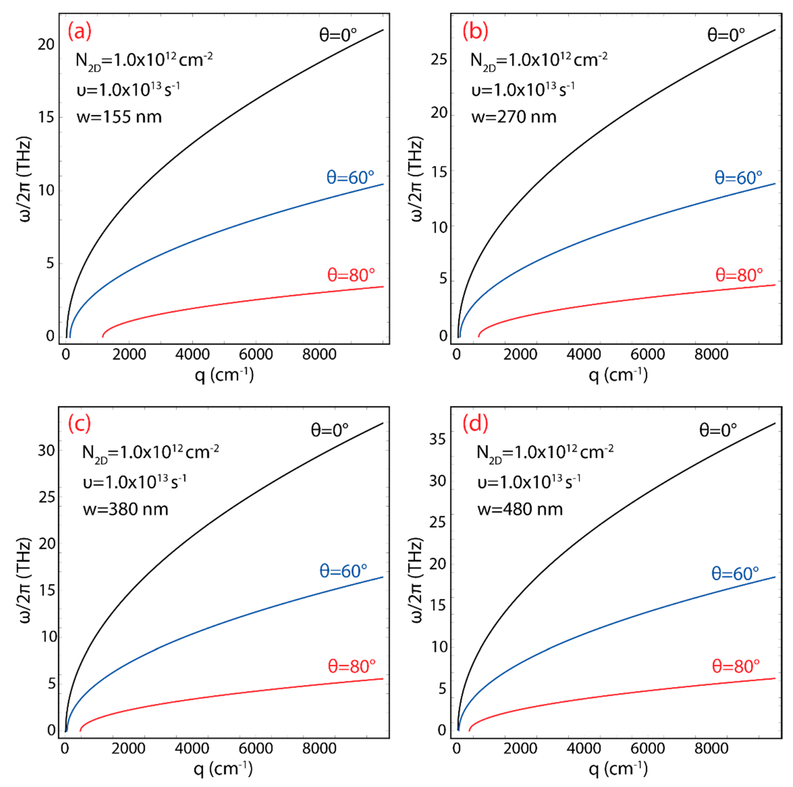
We now focus on the effect of the excitation angle. Figure 7 shows the plasmon frequency dispersion by taking different directions for the excitation wave vector: θ = 0 , θ = 60 , and θ = 80 , and different ribbon widths: w = 155 nm (Figure 7a), w = 270 nm (Figure 7b), w = 380 nm (Figure 7c), and w = 480 nm (Figure 7d). For comparison, we fix N 2 D = 1.0 × 10 12 cm−2 and ν = 1.0 × 10 13 s−1. Again, the plasmon frequency trend follows a q -like dispersion regardless of the excitation angle. The important finding is the fact that there is a momentum range for which no plasmons are allowed to exist.
As a notable example, at θ = 80 (red lines), no plasmons are detected at q < 1200 cm−1 for w = 155 nm, at q < 700 cm−1 for w = 270 nm, at q < 500 cm−1 for w = 380 nm, and at q < 400 cm−1 for w = 480 nm. Therefore, as the ribbon width increases, the momentum region for which the plasmon does not exist shrinks, suggesting that for w , the plasmon dispersion recovers the results of graphene, i.e., THz = 0 and q = 0 . Additionally, it is observed that the plasmon frequency increases by changing the ribbon width. Indeed, for the case of w = 155 nm (Figure 7a, black line), the entire frequency–momentum dispersion is about 20 THz, whereas, for the case of w = 480 nm (Figure 7d, black line) the entire plasmon dispersion is about 35 THz.
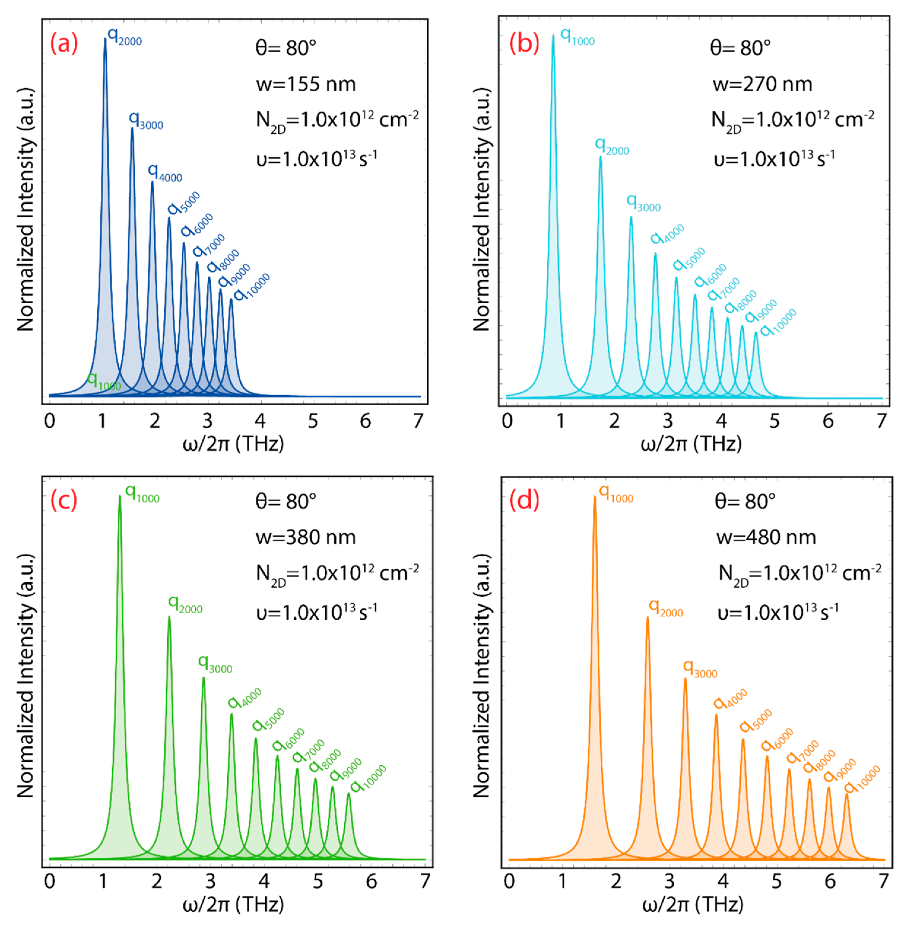
To further highlight the effect of the excitation angle at θ = 80 , the plasmon spectra for selected q values (from 1000 to 10,000 cm−1) and different ribbon widths are reported in Figure 8 and Table S6. Notably, no plasmons are detected at q = 1000 cm−1 for w = 155 nm (see Table S6, Figure 7a). The plasmon excitation peak is found from 1.05 to 3.43 THz for w = 155 nm (Figure 8a), from 0.87 to 4.65 THz for w = 270 nm (Figure 8b), from 1.31 to 5.58 THz for w = 380 nm (Figure 8c), and from 1.60 to 6.30 THz for w = 480 nm (Figure 8d).
Figure 9a–c show the plasmon spectra at θ = 80 for q = 2000 ,   5000 ,   10,000 cm−1 as a function of the ribbon width. From these results, we provide evidence for the sensibility of the plasmon response by increasing the ribbon width and showing that the plasmon peak mainly shifts to higher values of frequency in all cases. On the other hand, Figure 9d and Table S7 exhibit the greatest effect of the combination of the excitation angle and ribbon width occurring at small q values, say, q = 2000 cm−1 (Figure 9d, black curve). In fact, the plasmon frequency increases by ~40% for GNR arrays from 155 nm to 270 nm wide, by ~22% from 270 nm to 380 nm wide, and by ~14% from 380 nm to 480 nm wide. For the other values of q a similar situation is observed but with a lower percentage variation (red and green curves).

3.4. The Effect of Relaxation Rate on the Plasmonic Properties

Regarding the experimental part, the preparation process of graphene produces samples with different defects, such as sp3-defects, vacancy-like defects, and edge-type defects [42]. These defects can also be found in wide GNRs which are expected to modify their electronic and optical properties [43]. In line with the present work, high carrier mobility is usually observed in defect-free samples but as the density of the defects increases, the charge carrier mobility is reduced. This fact is precisely what we proceed to examine in Figure 10, by changing the electron relaxation rate ( ν ) due to a high ν value being connected with a higher density of defects, hence, a low charge carrier mobility. As an example, an electron relaxation rate of ν = 1.0 × 10 13 s−1 corresponds to an electron mobility of 50,000 cm2/V s whereas ν = 4.0 × 10 13 to ~ 22,100 cm2/V s.
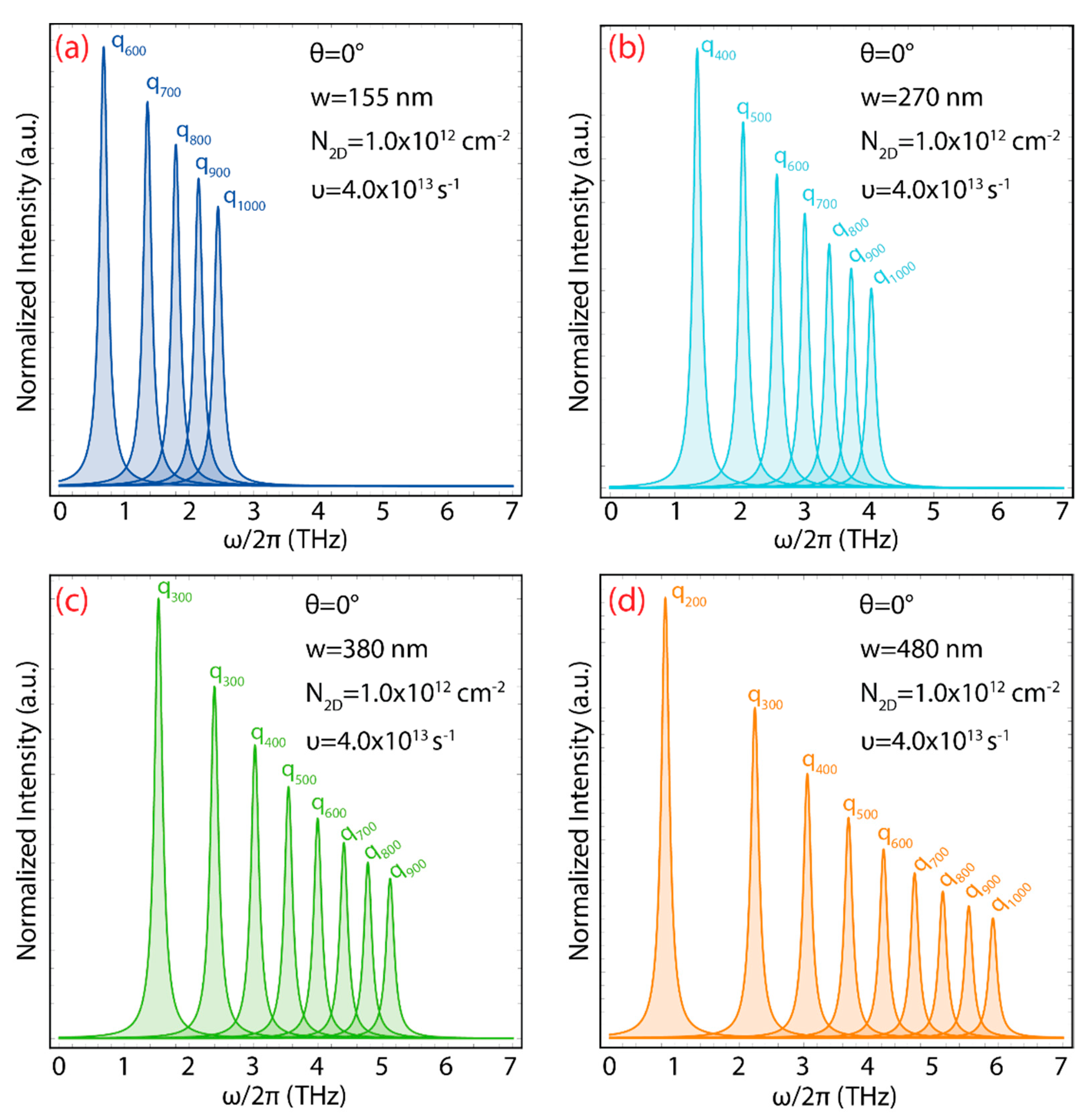
In this context, the sensitivity of the plasmon frequency dispersion is investigated using three values of the relaxation rate ( ν = 1.0 × 10 13 s−1, ν = 2.0 × 10 13 s−1, and ν = 4.0 × 10 13 s−1) and fixing the other parameters as: N 2 D = 1.0 × 10 12 cm−2 and θ = 0 . We point out that the horizontal axes of Figure 10 are ten times smaller, i.e., q 1000 cm−1. In all the GNR arrays, as the ν value increases, the frequency–momentum dispersion shifts toward larger values of q and furthermore, the plasmon frequency is reduced.
The interesting part of the results is the fact that there is a momentum range for which no plasmons are allowed to exist again, particularly, at ν = 2.0 × 10 13 s−1 (blue curves) and ν = 4.0 × 10 13 s−1 (red curves). The greatest effect of the electron relaxation rate is distinguished at ν = 4.0 × 10 13 s−1 where no plasmons are found at q < 550 cm−1 for w = 155 nm (Figure 10a), at q < 350 cm−1 for w = 270 nm (Figure 10b), at q < 250 cm−1 for w = 380 nm (Figure 10c), and at q < 200 cm−1 for w = 480 nm (Figure 10d). Consequently, as the ν value increases, the momentum region for which the plasmon does exist is enlarged.
To highlight the effect of the relaxation rate at ν = 4.0 × 10 13 s−1, the plasmon spectra for selected q values from 100 to 1000 cm−1 and different ribbon widths are reported in Figure 11 and Table S8. In particular, no plasmons are detected at 0 < q < 500 cm−1 for w = 155 nm (Figure 11a), at 0 < q < 300 cm−1 for w = 270 nm (Figure 11b), at 0 < q < 200 cm−1 for w = 380 nm (Figure 11c), and at 0 < q < 500 cm−1 for w = 480 nm (Figure 11d). Additionally, the plasmon excitation peak is detected from 0.69 to 2.45 THz for w = 155 nm, from 1.35 to 4.04 THz for w = 270 nm, from 1.53 to 5.11 THz for w = 380 nm, and from 0.86 to 5.92 THz for w = 480 nm.
On the other hand, Figure 12a–c displays the plasmon spectra at ν = 4.0 × 10 13 s−1 for q = 600 ,   800 ,   1000 cm−1 as a function of the ribbon width. Similarly, for all cases, the plasmon peak shifts to higher values of frequency by increasing the value of the ribbon width. Additionally, Figure 12d and Table S9 show that the greatest effect of the combination of the electron relaxation rate ( ν = 4.0 × 10 13 s−1) and ribbon width, particularly, occurs at q = 600 cm−1 (Figure 10d, black curve). The plasmon frequency increases by ~73% for GNR arrays from 155 nm to 270 nm wide, by ~27% from 270 nm to 380 nm wide, and by ~16% from 380 nm to 480 nm wide. Thus, we can conclude that the electron relaxation rate is a significant parameter in the conductivity-related phenomena of 2D GNR arrays which should be taken into account when designing new biosensors.

3.5. The Effect of 2D Carrier Concentration on the Plasmonic Properties

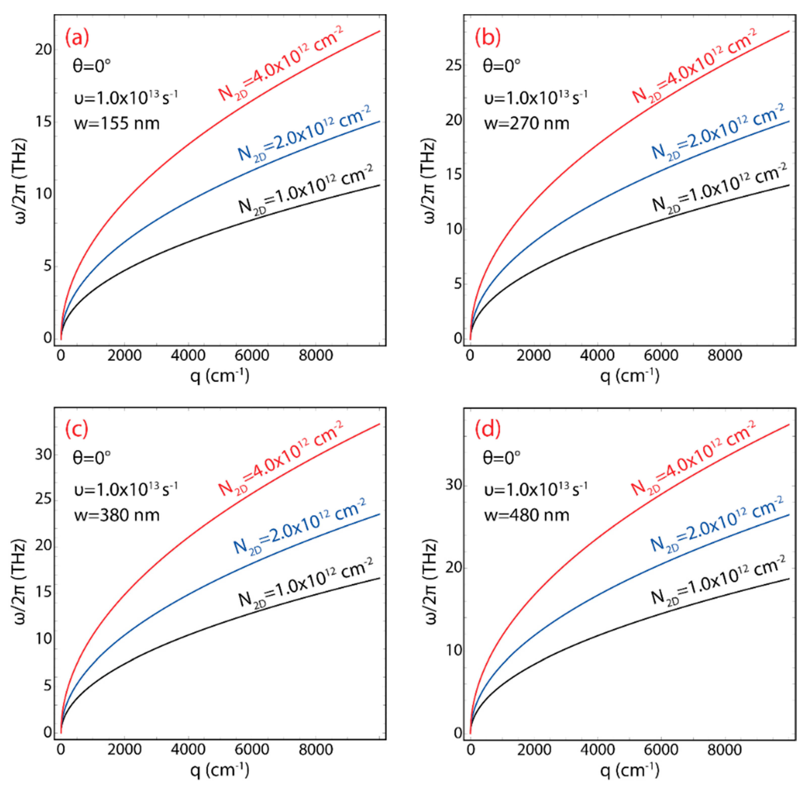
The final parameter to be controlled in Equation (4) is the 2D charge carrier concentration denoted as N 2 D . This effect can be commonly altered by injecting or ejecting electrons, i.e., by doping the GNRs or by a gating voltage. In particular, this quantity can be varied easily in a reasonable range up to N 2 D ~ 5.0 × 10 12 cm−2 [35]. Figure 13 shows precisely this effect on the plasmon frequency–momentum dispersion for each of the systems ( w = 155 nm (Figure 13a), w = 270 nm (Figure 13b), w = 380 nm (Figure 13c), and w = 480 nm (Figure 14d)) by using three reference N 2 D values ( N 2 D = 1.0 × 10 12 cm−2 (black curve), N 2 D = 1.0 × 10 12 cm−2 (blue curve), and N 2 D = 2.0 × 10 12 cm−2 (red curve)), and fixing: ν = 4.0 × 10 13 s−1 and θ = 0 .
Particularly, Figure 13 shows that increasing the value of N 2 D , the forbidden region for the plasmon becomes zero in other places where the value of the charge carrier density used in wide GNR arrays, i.e., the plasmon frequency–momentum dispersion, shifts towards q 0 . However, this effect is very dramatic for the plasmon frequency dispersion in all the analyzed cases because increasing the charge carrier density leads to an increase in the plasmon energy. As noticed, a significant increase in frequency is observed, by the comparison from ν = 1.0 × 10 13 s−1 to ν = 4.0 × 10 13 s−1 (red curves) of about 20 THz for the GNR arrays 155 nm wide (Figure 13a) to ~ 40 THz for 480 nm wide (Figure 13d). We point out that these results are below the limit of the semi-analytical model ( ~ 50 THz, Section 2.2), suggesting a good agreement between our predictions and future experiments.
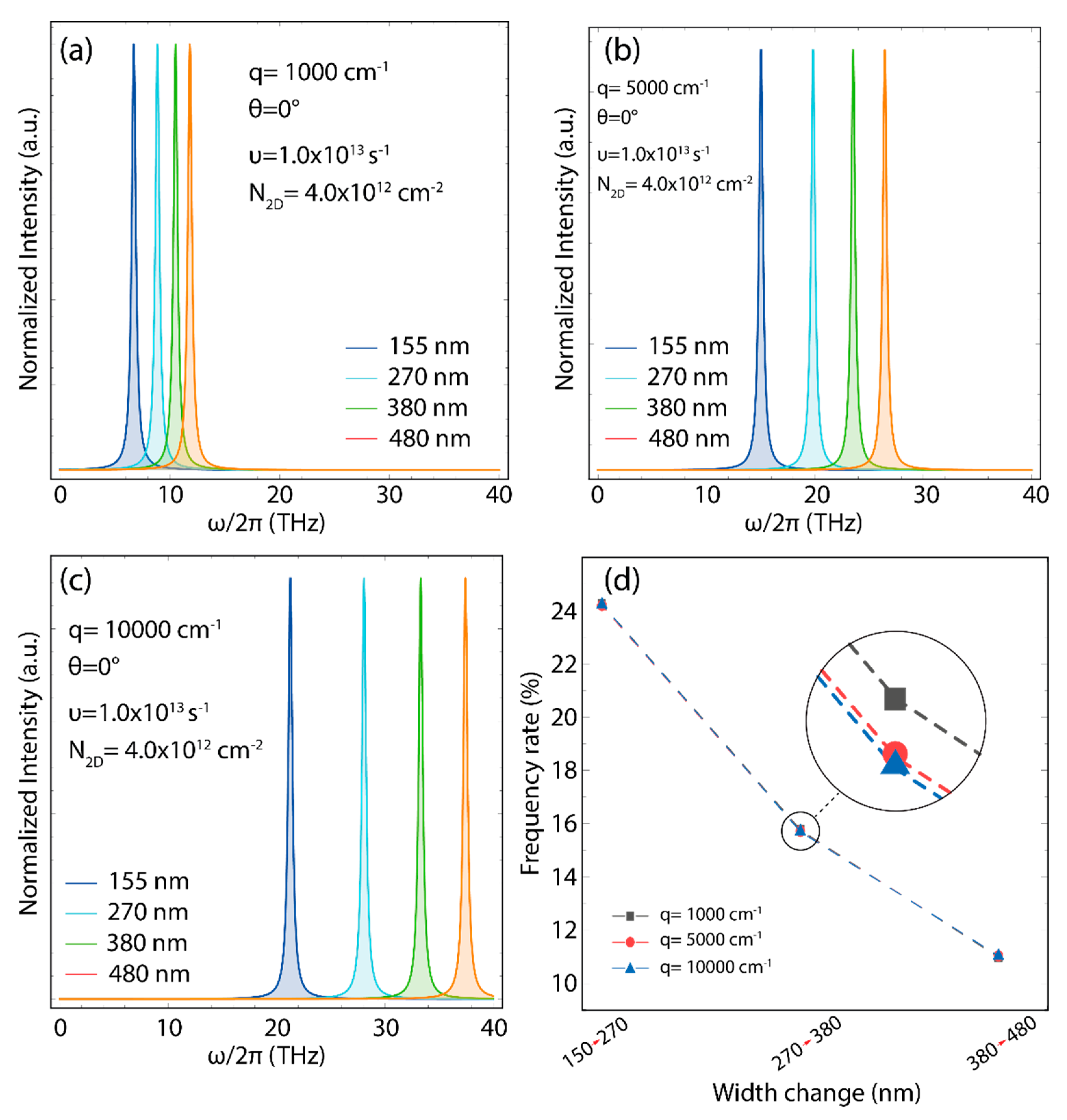
To scrutinize the crucial effect of the charge carrier density at N 2 D = 4.0 × 10 12 cm−2, the plasmon spectra for q values from 1000 to 10,000 cm−1 and different ribbons widths are reported in Figure 14 and Table S10. Interestingly enough, surface plasmons are detected at a frequency–momentum range of zero for all cases (Figure 13), i.e., the forbidden regions are absent. More importantly, the plasmon excitation peak is found from 6.72 to 21.26 THz for w = 155 nm (Figure 14a), from 8.87 to 28.06 THz for w = 270 nm (Figure 14b), from 10.53 to 33.29 THz for w = 380 nm (Figure 14c), and from 11.83 to 37.42 THz for w = 480 nm (Figure 14d).
Figure 15a–c presents the plasmon spectra at N 2 D = 4.0 × 10 12 cm−2 for q = 1000 ,   5000 ,   10,000 cm−1 as a function of the ribbon width. As evidenced, the 2D charge density is the most critical parameter to substantially increase the plasmon frequency because the plasmon peak shifts, for instance, from 21 THz (at q = 10,000 cm−1 and w = 155 nm) to 37.42 THz (at q = 10,000 cm−1 and w = 480 nm). Lastly, regardless of the value of q , Figure 15d and Table S11 show that the combined effect of the 2D charge carrier density and ribbon width increased the plasmon frequency by ~ 24% for the 2D GNR arrays from 155 nm to 270 nm wide, by ~ 16% from 270 nm to 380 nm wide, and by ~ 11% from 380 nm to 480 nm wide.

4. Potential Applications of Wide 2D GNR Arrays in Biosensors

All the results presented in the previous section are very relevant because they suggest that precise control of the plasmonic response is possible using wide graphene nanoribbons and by combining different technical parameters to adapt to a specific demand of graphene-based biosensors. With this in mind, we proceed to discuss our results in terms of some potential applications, such as molecular sensing.

4.1. Detection of Lactose Molecules

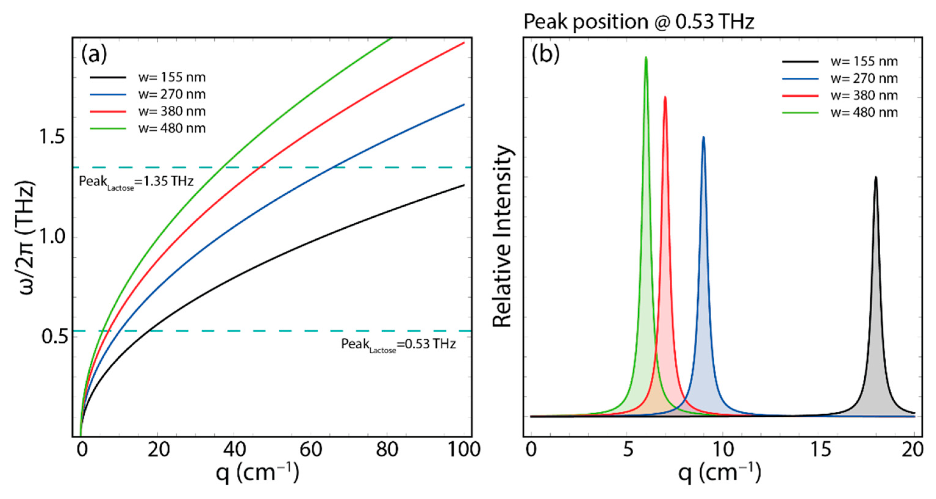
Very recently, Choi G., et al. [44] reported the fabrication of a graphene/metallic nanoslot antenna for the molecular detection of lactose molecules as prototypical biomolecules which have intermolecular absorption in the THz regime. Specifically, the lactose molecules have weak and strong peaks at 0.53 THz and 1.35 THz, respectively. In terms of sensitivity, the peak at 0.53 THz has a smaller absorption coefficient, making it difficult to detect. Hence, all the analyzed 2D GNR arrays become interesting candidates for ultrasensitive molecular detection because of the enhanced electric field due to the one-dimensional confinement, and more importantly, these systems have resonance modes at the same THz scale working on lower q values ( q 100 cm−1). The latter is shown in Figure 16a by setting N 2 D = 1.0 × 10 12 cm−2, θ = 0 , and ν = 0.0 s−1.
In all cases, plasmon responses are observed at 0.53 THz; however, only the widest ribbons give plasmonic responses at 1.35 THz, i.e., w = 270 (blue curve), w = 380 (red curve), and w = 480 (green curve). Note that we are using ν = 0 , which means defect-free GNR samples, resulting in the highest possible electron mobility. Another important result is the fact that although all 2D GNR arrays have plasmon responses at 0.53 THz, these resonances are found at different values of momentum ( q ); for instance, for w = 155 nm wide, the peak is found at q 18 cm−1 (Figure 16b, black curve) whereas for w = 480 nm wide, the peak is found at q 6 cm−1 (Figure 16b, green curve).

4.2. Detection of Molecules in Water

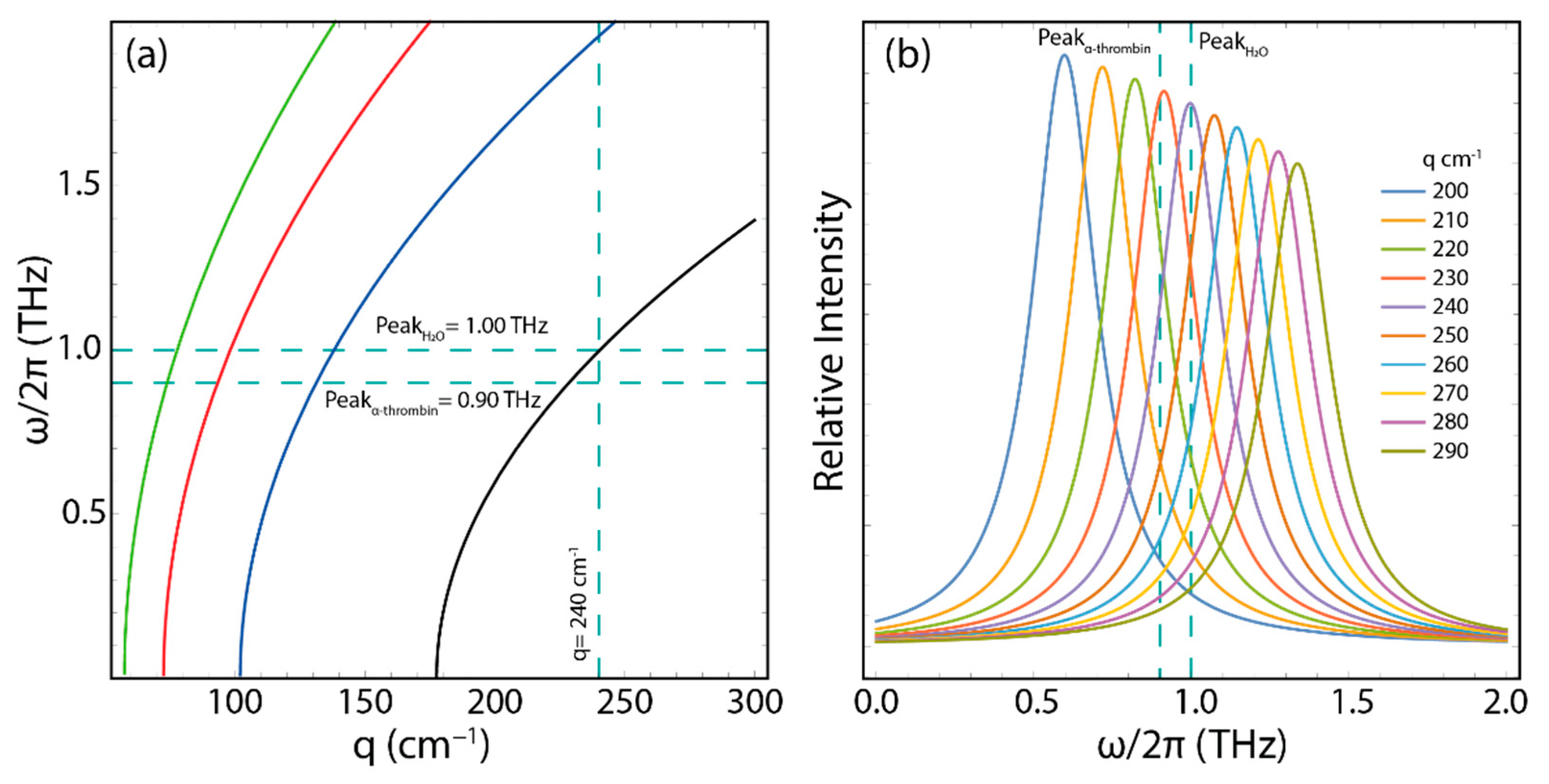
In clinical analysis, a significant problem is the identification of pure aqueous molecules because water generates strong THz absorption at 1 THz and q 240 cm−1 [45] which severely obscures the response of solute molecules, leading to similar absorption features for different trace molecules. To weaken the interference of water, sample preparation requires a tedious drying process or the replacement of water with a low-absorption medium; however, this is not possible in all cases. In this context, THz nanomaterials with obvious resonance peaks in the water frequency-absorption range could greatly enhance the interactions between incident THz waves and adherent target molecules, demonstrating practical applications in sensing proteins, nucleic acids, and cells. This fact is confirmed in Figure 17 by setting N 2 D = 1.0 × 10 12 cm−2, θ = 0 , and ν = 2.24 s−1.
Note that we now use even a high value of the electron relaxation rate ( ν ) to be able to achieve the desired frequency (1 THz) and momentum range ( q 240 cm−1), suggesting that GNRs with a high defect density (such as oxidized graphene ribbons) could be the best choice for detecting aqueous molecules. Figure 17a demonstrates that this issue can be solved using 2D GNR arrays 155 nm wide (black curve), setting the possibility of assembling optimized THz biosensors to sense, for instance, human α-thrombin whose resonance peak is detected at about 0.9 THz [45]. In response to this, Figure 17b displays the existence of plasmon resonance modes in 2D GNR arrays 155 nm wide in the same THz frequency of water at q = 240 cm−1 (purple curve) and α-thrombin at q = 229 cm−1 (red curve).

4.3. Detection of Chlorpyrifos-Methyl Molecules

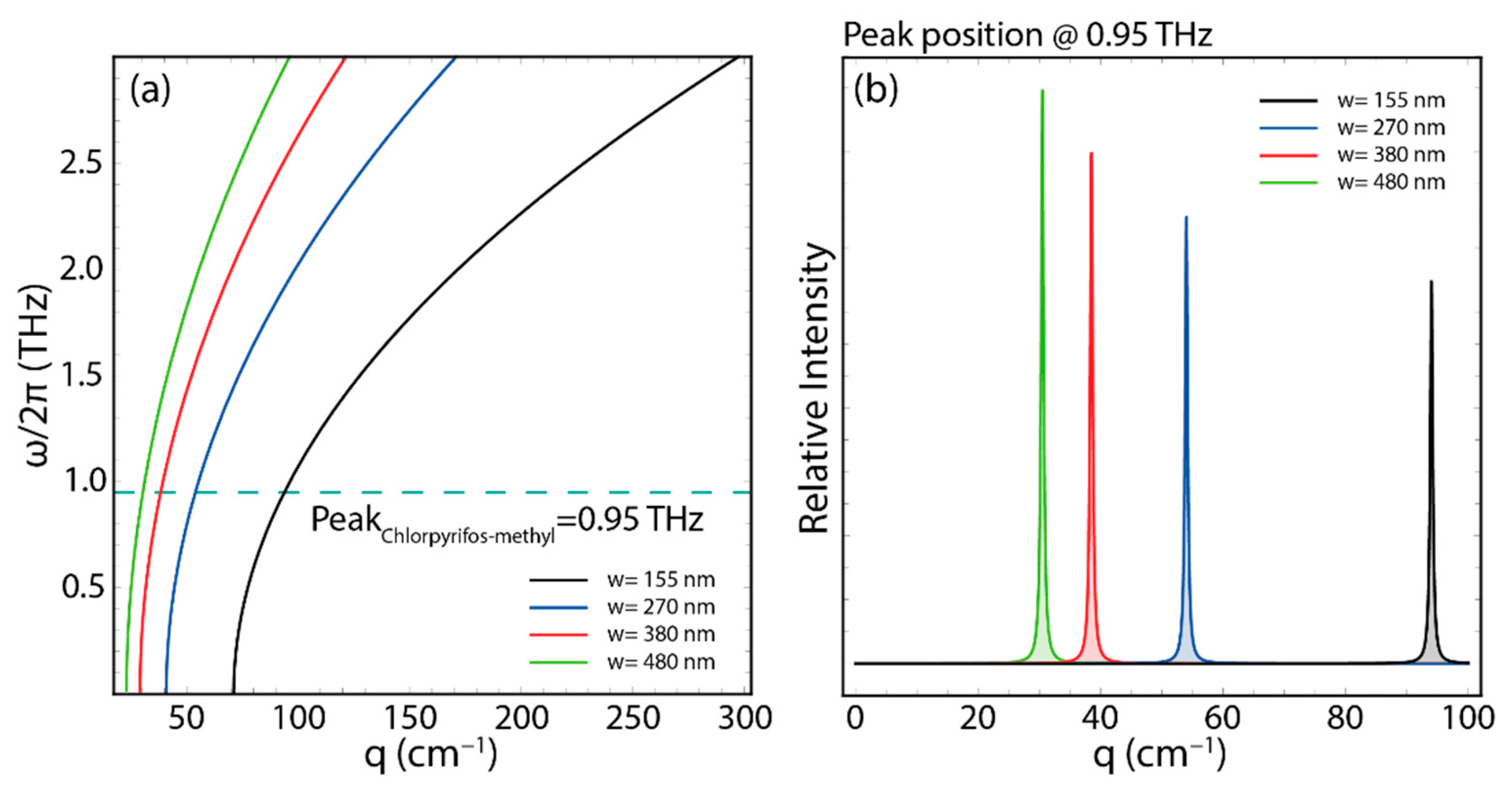
In cases in which the samples can be dried, one of the most interesting physical properties of graphene can be used, which is also present in wide 2D GNR arrays, i.e., the out-of-plane π electrons. As an example, the chlorpyrifos-methyl molecule is an insecticide mainly used to control insect pests on a range of crops. However, this pesticide is highly toxic to organisms and humans, requiring urgent detection methods and removal techniques. Regarding the chemical structure conformation, chlorpyrifos-methyl has a benzene-like ring with π electrons, which are expected to have a direct interaction with the π electrons of GNRs through π π stacking, and furthermore, this molecule has a resonance peak at 0.95 THz [46]. The following is illustrated in Figure 18 by setting N 2 D = 2.5 × 10 12 cm−2, θ = 0 , and ν = 2.24 s−1.
Precisely, all the analyzed 2D GNR arrays offer the required THz response at these frequencies (Figure 18a), demonstrating their application in label-free sensing. Note that we are using high values of the electron relaxation rate ( ν ) and charge carrier concentration ( N 2 D ), which in turn demonstrates two important facts: (i) the use of GNR samples with a high density of defects; and (ii) a charge transfer from the molecule (doping) is expected due to the interaction between the 2D GNR array and chlorpyrifos-methyl molecule via the π π interactions. Additionally, an important result is the fact that although all 2D GNR arrays have plasmon responses at 0.95 THz, these resonance modes shift to lower values of momentum ( q ); for instance, for w = 155 nm wide, the peak position at 0.95 THz is found at q 94 cm−1 (Figure 18b, black curve) whereas for w = 480 nm wide the peak position is found at q 30 cm−1 (Figure 18b, green curve).

4.4. Detection of Glucose and Malaria

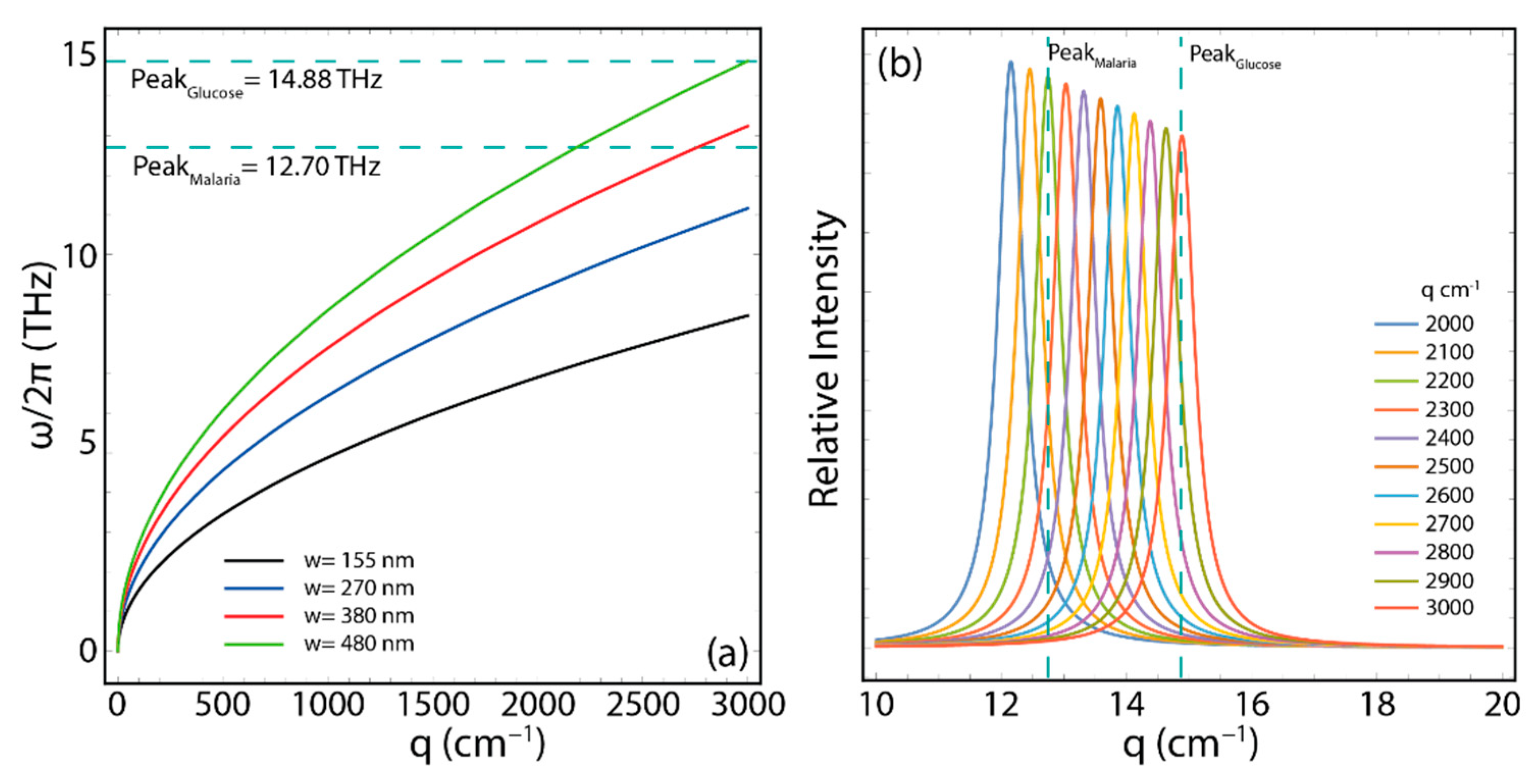
Last but not least, materials with specific ranges of physical parameters, such as permittivity and permeability, are needed for high-frequency sensing applications. The purpose of these materials is the implementation of ultrathin, ultrasensitive, and absorption-based biosensors with a narrowband THz response. The required features are covered by the 2D GNR arrays examined here. As evidenced throughout our present work, GNRs have interesting tunability and controllability in the frequency of interest. In particular, the excitation of surface plasmons in 2D GNR arrays causes strong field confinement which results in a perfect absorption spectrum. As illustrative examples, glucose in water and malaria in blood have resonances at 14.88 and 12.7 THz, respectively [47]. These resonance modes are investigated in Figure 19 by setting N 2 D = 1.5 × 10 12 cm−2, θ = 0 , and ν = 0.0 s−1. Here we propose the use of defect-free GNR samples and we increase the value of the charge carrier density a little bit since the latter is expected as an effect of the charge transfer from the molecules to the 2D GNR arrays.
Interestingly enough, 2D GNR arrays 480 nm wide (Figure 19a, green curve) show similar THz excitation peaks, confirming the prospect of building excellent adsorbers that can be utilized as faultless absorption platforms working at the frequency of higher-order resonance. On the other hand, 2D GNR arrays 380 nm wide show resonance modes below 14 THz, suggesting their use for detecting malaria in blood but not glucose in water. Nevertheless, this fact is relative, since depending on the type of molecule, the interaction could be stronger (see the discussion in the previous section, Section 4.3), causing a larger charge transfer, which performs in larger doping of 2D GNR arrays. Indeed, even the other 2D GNRs arrays (e.g., w = 270 nm) could also be candidates for the detection of glucose and malaria. Figure 19b confirms the presence of plasmon resonance modes in the same frequency of glucose at q = 2200 cm−1 (green curve) and malaria at q = 3000 cm−1 (red curve).

5. Conclusions

In summary, we have presented a semi-analytical approach based on the charge carrier velocity of graphene to study the plasmonic properties of experimentally realized 2D GNR arrays with widths ranging from 155 to 480 nm within the THz scale, and considering freestanding systems, for instance, GNRs on insulating substrates.
This simple model allows us to analyze the trends of surface plasmon’s characteristics in 2D GNR arrays, for which an ab initio approach is unworkable. Our study provided a complete picture of controlling the plasmon frequency dispersion and plasmon response. In particular, the surface plasmon modes are strongly dependent on the ribbon width and experimental setup.
As main results:
  • The analyzed systems show bandgap values from 22.12 to 7.14 meV.
  • Several sub-bands are observed in the equal energy region as the ribbon width increases.
  • All GNR systems display a direct bandgap at the K point.
  • An interesting outcome is the fact that increasing the ribbon width increases the plasmon frequency dispersion.
  • At excitation angles of θ = 80, no plasmons are detected at q = 0.
  • At higher values of v, the entire plasmon frequency–momentum dispersion is significantly reduced with the presence of forbidden regions for plasmons.
  • The combination of ribbon width and 2D charge concentration increases the plasmon frequency up to about 40 THz.
Additionally, we have evidenced the possibility of using the scrutinized 2D GNR arrays in molecular sensing. Particular attention is given to the detection and sensing of:
  • Lactose molecules;
  • Human α-thrombin;
  • Chlorpyrifos-methyl;
  • Glucose in water;
  • Malaria in blood.
Our findings are very relevant because they suggest that precise control of the plasmonic response is possible in the case of wide nanoribbons by combining different technical parameters to fit a specific demand for future biosensors based on graphene or materials beyond graphene [48].

Supplementary Materials

The following supporting information can be downloaded at: https://www.mdpi.com/article/10.3390/chemosensors10120514/s1, Figure S1: Experimentally realized graphene nanoribbons organized as 2D periodic arrays for (a) w = 155 nm, (b) w = 270 nm, (c) w = 380 nm and (d) w = 380 nm (Ref. [1]); Figure S2: (a) Band structure of graphene in the vicinity of Κ point with the Fermi level set to zero energy. The blue line is the π band and the red line is the π * band. (b) Fermi velocity as a function of the single-particle energy for the π band (blue circles) and the π * band (darker red circles) in the k -point region; Figure S3: (a) Bandgap ( Δ ) as a function of the ribbon width ( w ). Markers represent the GNR systems under study and the dashed lines are the fitting curve using Equation (2). The numerical values of the bandgap are calculated using different charge carrier velocities as reported in Ref. [2]. (b) Plasmon frequency dispersion ( ω / 2 π ) vs. wave vector ( q ) for 2D GNR arrays of w = 270 nm wide. The parameters of Equation (4) have been fixed as: N 2 D = 1.0 × 10 12 cm−2, θ = 0 , ν = 1.0 × 10 13 s−1, and different carrier velocities are considered; Table S1: Computed k -points and single-particle energies using LDA-DFT for the π and π * bands close to the Κ point. Calculated Fermi velocity by Equation (2); Table S2: Bandgap and charge carrier effective mass of GNRs with ribbon width: w = 155 ,   270 ,   380 ,   480 nm. The free-electron mass is denoted as m 0 . The charge carrier velocity is v F = 0.829 × 10 6 m/s; Table S3: Bandgap and charge carrier effective mass of GNRs with ribbon width: w = 155 ,   270 ,   380 ,   480 nm. The free-electron mass is denoted as m 0 . The charge carrier velocity is v F 1.0 × 10 6 m/s; Table S4: Peak position of plasmon response in 2D GNR arrays of 155, 270, 380, and 480 nm wide, selecting three different q values ( q = 100 , 1000 , 10,000 cm−1); Table S5: Percentage increase in plasmon frequency by increasing ribbon width for three different q values ( q = 100 , 1000 , 10,000 cm−1); Table S6: Peak position of plasmon response in 2D GNR arrays of 155, 270, 380, and 480 nm wide, for selected q values at θ = 80 ; Table S7: Percentage increase in plasmon frequency by increasing ribbon width for three different q values ( q = 2000 , 5000 , 10,000 cm−1) at θ = 80 ; Table S8: Peak position of plasmon response in 2D GNR arrays of 155, 270, 380, and 480 nm wide, for selected q values at ν = 4.0 × 10 13 s−1; Table S9: Percentage increase in plasmon frequency by increasing ribbon width for three different q values ( q = 600 , 800 , 1000 cm−1) at ν = 4.0 × 10 13 s−1; Table S10: Peak position of plasmon response in 2D GNR arrays of 155, 270, 380, and 480 nm wide, for selected q values at N 2 D = 4.0 × 10 12 cm−2; Table S11: Percentage increase in plasmon frequency by increasing ribbon width for three different q values ( q = 600 , 800 , 1000 cm−1) at N 2 D = 4.0 × 10 12 cm−2. References [28,38] are cited in the supplementary materials.

Author Contributions

Conceptualization, C.V.G.; methodology, J.S. and C.V.G.; validation, T.T. and M.G.; investigation, D.C.-F., J.B. and C.V.G.; resources, T.T.; data curation, T.T. and M.G.; supervision, C.V.G.; writing—original draft preparation, T.T., J.S. and C.V.G.; writing—review and editing, C.V.G.; visualization, M.G. All authors have read and agreed to the published version of the manuscript.

Funding

This work was supported by Universidad Técnica Particular de Loja (UTPL-Ecuador) (RUC No. 1190068729001).

Institutional Review Board Statement

Not applicable.

Informed Consent Statement

Not applicable.

Data Availability Statement

Not applicable.

Acknowledgments

T.T.: M.G., and C.V.G. wish to thank the Ecuadorian National Department of Sciences and Technology (SENESCYT). Part of this work has been also supported by the project “Desarrollo y optimización de métodos analíticos para la extracción y cuantificación de polifenoles en matrices vegetales” (grant no. PIV-66-2021).

Conflicts of Interest

The authors declare no conflict of interest.

References

  1. Toudert, J.; Serna, R. Interband Transitions in Semi-Metals, Semiconductors, and Topological Insulators: A New Driving Force for Plasmonics and Nanophotonics. Opt. Mater. Express 2017, 7, 2299–2325. [Google Scholar] [CrossRef]
  2. Gan, C.H.; Gbur, G.; Visser, T.D. Surface Plasmons Modulate the Spatial Coherence of Light in Young’s Interference Experiment. Phys. Rev. Lett. 2007, 98, 43908. [Google Scholar] [CrossRef] [PubMed]
  3. Zhang, Z.; Deckert-Gaudig, T.; Singh, P.; Deckert, V. Single Molecule Level Plasmonic Catalysis—A Dilution Study of p-Nitrothiophenol on Gold Dimers. Chem. Commun. 2015, 51, 3069–3072. [Google Scholar] [CrossRef] [PubMed] [Green Version]
  4. Atwater, H.A.; Polman, A. Plasmonics for Improved Photovoltaic Devices. Nat. Mater. 2010, 9, 205–213. [Google Scholar] [CrossRef]
  5. Bellassai, N.; D’Agata, R.; Jungbluth, V.; Spoto, G. Surface Plasmon Resonance for Biomarker Detection: Advances in Non-Invasive Cancer Diagnosis. Front. Chem. 2019, 7, 570. [Google Scholar] [CrossRef] [PubMed] [Green Version]
  6. Panoiu, N.C.; Sha, W.E.I.; Lei, D.Y.; Li, G.C. Nonlinear Optics in Plasmonic Nanostructures. J. Opt. 2018, 20, 83001. [Google Scholar] [CrossRef] [Green Version]
  7. Wang, H. Plasmonic Refractive Index Sensing Using Strongly Coupled Metal Nanoantennas: Nonlocal Limitations. Sci. Rep. 2018, 8, 9589. [Google Scholar] [CrossRef] [Green Version]
  8. Coello-Fiallos, D.; Tene, T.; Guayllas, J.L.; Haro, D.; Haro, A.; Gomez, C.V. DFT Comparison of Structural and Electronic Properties of Graphene and Germanene: Monolayer and Bilayer Systems. Mater. Today Proc. 2017, 4, 6835–6841. [Google Scholar] [CrossRef]
  9. Gomez, C.V.; Robalino, E.; Haro, D.; Tene, T.; Escudero, P.; Haro, A.; Orbe, J. Structural and Electronic Properties of Graphene Oxide for Different Degree of Oxidation. Mater. Today Proc. 2016, 3, 796–802. [Google Scholar] [CrossRef]
  10. Scarcello, A.; Alessandro, F.; Polanco, M.A.; Gomez, C.V.; Perez, D.C.; De Luca, G.; Curcio, E.; Caputi, L.S. Evidence of Massless Dirac Fermions in Graphitic Shells Encapsulating Hollow Iron Microparticles. Appl. Surf. Sci. 2021, 546, 149103. [Google Scholar] [CrossRef]
  11. Sindona, A.; Pisarra, M.; Gomez, C.V.; Riccardi, P.; Falcone, G.; Bellucci, S. Calibration of the Fine-Structure Constant of Graphene by Time-Dependent Density-Functional Theory. Phys. Rev. B 2017, 96, 201408. [Google Scholar] [CrossRef]
  12. Sindona, A.; Vacacela Gomez, C.; Pisarra, M. Dielectric Screening versus Geometry Deformation in Two-Dimensional Allotropes of Silicon and Germanium. Sci. Rep. 2022, 12, 15107. [Google Scholar] [CrossRef] [PubMed]
  13. Gomez, C.V.; Pisarra, M.; Gravina, M.; Riccardi, P.; Sindona, A. Plasmon Properties and Hybridization Effects in Silicene. Phys. Rev. B 2017, 95, 85419. [Google Scholar] [CrossRef] [Green Version]
  14. Wu, L.; Chu, H.-S.; Koh, W.S.; Li, E.-P. Highly Sensitive Graphene Biosensors Based on Surface Plasmon Resonance. Opt. Express 2010, 18, 14395–14400. [Google Scholar] [CrossRef] [PubMed]
  15. Fu, H.; Zhang, S.; Chen, H.; Weng, J. Graphene Enhances the Sensitivity of Fiber-Optic Surface Plasmon Resonance Biosensor. IEEE Sens. J. 2015, 15, 5478–5482. [Google Scholar] [CrossRef]
  16. Sadeghi, Z.; Shirkani, H. Highly Sensitive Mid-Infrared SPR Biosensor for a Wide Range of Biomolecules and Biological Cells Based on Graphene-Gold Grating. Phys. E Low-Dimens. Syst. Nanostructures 2020, 119, 114005. [Google Scholar] [CrossRef]
  17. Zhang, H.; Song, D.; Gao, S.; Zhang, J.; Zhang, H.; Sun, Y. Novel SPR Biosensors Based on Metal Nanoparticles Decorated with Graphene for Immunoassay. Sens. Actuators B Chem. 2013, 188, 548–554. [Google Scholar] [CrossRef]
  18. Mulpur, P.; Podila, R.; Lingam, K.; Vemula, S.K.; Ramamurthy, S.S.; Kamisetti, V.; Rao, A.M. Amplification of Surface Plasmon Coupled Emission from Graphene--Ag Hybrid Films. J. Phys. Chem. C 2013, 117, 17205–17210. [Google Scholar] [CrossRef]
  19. Ling, X.; Xie, L.; Fang, Y.; Xu, H.; Zhang, H.; Kong, J.; Dresselhaus, M.S.; Zhang, J.; Liu, Z. Can Graphene Be Used as a Substrate for Raman Enhancement? Nano Lett. 2010, 10, 553–561. [Google Scholar] [CrossRef]
  20. Low, T.; Avouris, P. Graphene Plasmonics for Terahertz to Mid-Infrared Applications. ACS Nano 2014, 8, 1086–1101. [Google Scholar] [CrossRef] [PubMed]
  21. Pisarra, M.; Sindona, A.; Riccardi, P.; Silkin, V.M.; Pitarke, J.M. Acoustic Plasmons in Extrinsic Free-Standing Graphene. New J. Phys. 2014, 16, 83003. [Google Scholar] [CrossRef] [Green Version]
  22. Pisarra, M.; Sindona, A.; Gravina, M.; Silkin, V.M.; Pitarke, J.M. Dielectric Screening and Plasmon Resonances in Bilayer Graphene. Phys. Rev. B 2016, 93, 35440. [Google Scholar] [CrossRef] [Green Version]
  23. Goldflam, M.D.; Fei, Z.; Ruiz, I.; Howell, S.W.; Davids, P.S.; Peters, D.W.; Beechem, T.E. Designing Graphene Absorption in a Multispectral Plasmon-Enhanced Infrared Detector. Opt. Express 2017, 25, 12400–12408. [Google Scholar] [CrossRef]
  24. Li, Y.; Yan, H.; Farmer, D.B.; Meng, X.; Zhu, W.; Osgood, R.M.; Heinz, T.F.; Avouris, P. Graphene Plasmon Enhanced Vibrational Sensing of Surface-Adsorbed Layers. Nano Lett. 2014, 14, 1573–1577. [Google Scholar] [CrossRef] [PubMed]
  25. Villamagua, L.; Carini, M.; Stashans, A.; Gomez, C.V. Band Gap Engineering of Graphene through Quantum Confinement and Edge Distortions. Ric. Mat. 2016, 65, 579–584. [Google Scholar] [CrossRef]
  26. Gomez, C.V.; Pisarra, M.; Gravina, M.; Sindona, A. Tunable Plasmons in Regular Planar Arrays of Graphene Nanoribbons with Armchair and Zigzag-Shaped Edges. Beilstein J. Nanotechnol. 2017, 8, 172–182. [Google Scholar] [CrossRef] [PubMed] [Green Version]
  27. Son, Y.-W.; Cohen, M.L.; Louie, S.G. Energy Gaps in Graphene Nanoribbons. Phys. Rev. Lett. 2006, 97, 216803. [Google Scholar] [CrossRef] [Green Version]
  28. Fei, Z.; Goldflam, M.D.; Wu, J.-S.; Dai, S.; Wagner, M.; McLeod, A.S.; Liu, M.K.; Post, K.W.; Zhu, S.; Janssen, G.; et al. Edge and Surface Plasmons in Graphene Nanoribbons. Nano Lett. 2015, 15, 8271–8276. [Google Scholar] [CrossRef] [Green Version]
  29. Gomez, C.V.; Pisarra, M.; Gravina, M.; Pitarke, J.M.; Sindona, A. Plasmon Modes of Graphene Nanoribbons with Periodic Planar Arrangements. Phys. Rev. Lett. 2016, 117, 116801. [Google Scholar] [CrossRef] [Green Version]
  30. Sindona, A.; Pisarra, M.; Bellucci, S.; Tene, T.; Guevara, M.; Gomez, C.V. Plasmon Oscillations in Two-Dimensional Arrays of Ultranarrow Graphene Nanoribbons. Phys. Rev. B 2019, 100, 235422. [Google Scholar] [CrossRef]
  31. Tene, T.; Guevara, M.; Viteri, E.; Maldonado, A.; Pisarra, M.; Sindona, A.; Vacacela Gomez, C.; Bellucci, S. Calibration of Fermi Velocity to Explore the Plasmonic Character of Graphene Nanoribbon Arrays by a Semi-Analytical Model. Nanomaterials 2022, 12, 2028. [Google Scholar] [CrossRef] [PubMed]
  32. Gomez, C.V.; Guevara, M.; Tene, T.; Lechon, L.S.; Merino, B.; Brito, H.; Bellucci, S. Energy Gap in Graphene and Silicene Nanoribbons: A Semiclassical Approach. In Proceedings of the AIP Conference Proceedings; AIP Publishing LLC.: Melville, NY, USA, 8 August 2018; Volume 2003, p. 020015. [Google Scholar]
  33. Popov, V.V.; Bagaeva, T.Y.; Otsuji, T.; Ryzhii, V. Oblique Terahertz Plasmons in Graphene Nanoribbon Arrays. Phys. Rev. B 2010, 81, 73404. [Google Scholar] [CrossRef]
  34. Barone, V.; Hod, O.; Scuseria, G.E. Electronic Structure and Stability of Semiconducting Graphene Nanoribbons. Nano Lett. 2006, 6, 2748–2754. [Google Scholar] [CrossRef]
  35. Han, M.Y.; Özyilmaz, B.; Zhang, Y.; Kim, P. Energy Band-Gap Engineering of Graphene Nanoribbons. Phys. Rev. Lett. 2007, 98, 206805. [Google Scholar] [CrossRef] [Green Version]
  36. Egerton, R.F. Electron Energy-Loss Spectroscopy in the TEM. Rep. Prog. Phys. 2008, 72, 16502. [Google Scholar] [CrossRef]
  37. Kohn, W. Density-Functional Theory for Excited States in a Quasi-Local-Density Approximation. Phys. Rev. A 1986, 34, 737. [Google Scholar] [CrossRef]
  38. Hwang, C.; Siegel, D.A.; Mo, S.-K.; Regan, W.; Ismach, A.; Zhang, Y.; Zettl, A.; Lanzara, A. Fermi Velocity Engineering in Graphene by Substrate Modification. Sci. Rep. 2012, 2, 590. [Google Scholar] [CrossRef] [Green Version]
  39. Whelan, P.R.; Shen, Q.; Zhou, B.; Serrano, I.G.; Kamalakar, M.V.; Mackenzie, D.M.A.; Ji, J.; Huang, D.; Shi, H.; Luo, D.; et al. Fermi Velocity Renormalization in Graphene Probed by Terahertz Time-Domain Spectroscopy. 2D Mater. 2020, 7, 35009. [Google Scholar] [CrossRef]
  40. Yan, H.; Xia, F.; Li, Z.; Avouris, P. Plasmonics of Coupled Graphene Micro-Structures. New J. Phys. 2012, 14, 125001. [Google Scholar] [CrossRef] [Green Version]
  41. Hajati, Y. Tunable Broadband Multiresonance Graphene Terahertz Sensor. Opt. Mater. 2020, 101, 109725. [Google Scholar] [CrossRef]
  42. Eckmann, A.; Felten, A.; Mishchenko, A.; Britnell, L.; Krupke, R.; Novoselov, K.S.; Casiraghi, C. Probing the Nature of Defects in Graphene by Raman Spectroscopy. Nano Lett. 2012, 12, 3925–3930. [Google Scholar] [CrossRef] [PubMed] [Green Version]
  43. Guo, H.; Wang, J. Effect of Vacancy Defects on the Vibration Frequency of Graphene Nanoribbons. Nanomaterials 2022, 12, 764. [Google Scholar] [CrossRef] [PubMed]
  44. Choi, G.; Hong, S.J.; Bahk, Y.-M. Graphene-Assisted Biosensing Based on Terahertz Nanoslot Antennas. Sci. Rep. 2019, 9, 9749. [Google Scholar] [CrossRef] [PubMed] [Green Version]
  45. Zhou, J.; Zhao, X.; Huang, G.; Yang, X.; Zhang, Y.; Zhan, X.; Tian, H.; Xiong, Y.; Wang, Y.; Fu, W. Molecule-Specific Terahertz Biosensors Based on an Aptamer Hydrogel-Functionalized Metamaterial for Sensitive Assays in Aqueous Environments. ACS Sensors 2021, 6, 1884–1890. [Google Scholar] [CrossRef]
  46. Xu, W.; Xie, L.; Zhu, J.; Tang, L.; Singh, R.; Wang, C.; Ma, Y.; Chen, H.-T.; Ying, Y. Terahertz Biosensing with a Graphene-Metamaterial Heterostructure Platform. Carbon N. Y. 2019, 141, 247–252. [Google Scholar] [CrossRef]
  47. Varshney, G.; Giri, P. Bipolar Charge Trapping for Absorption Enhancement in a Graphene-Based Ultrathin Dual-Band Terahertz Biosensor. Nanoscale Adv. 2021, 3, 5813–5822. [Google Scholar] [CrossRef]
  48. Pisarra, M.; Gomez, C.V.; Sindona, A. Massive and Massless Plasmons in Germanene Nanosheets. Sci. Rep. 2022, 12, 18624. [Google Scholar] [CrossRef]
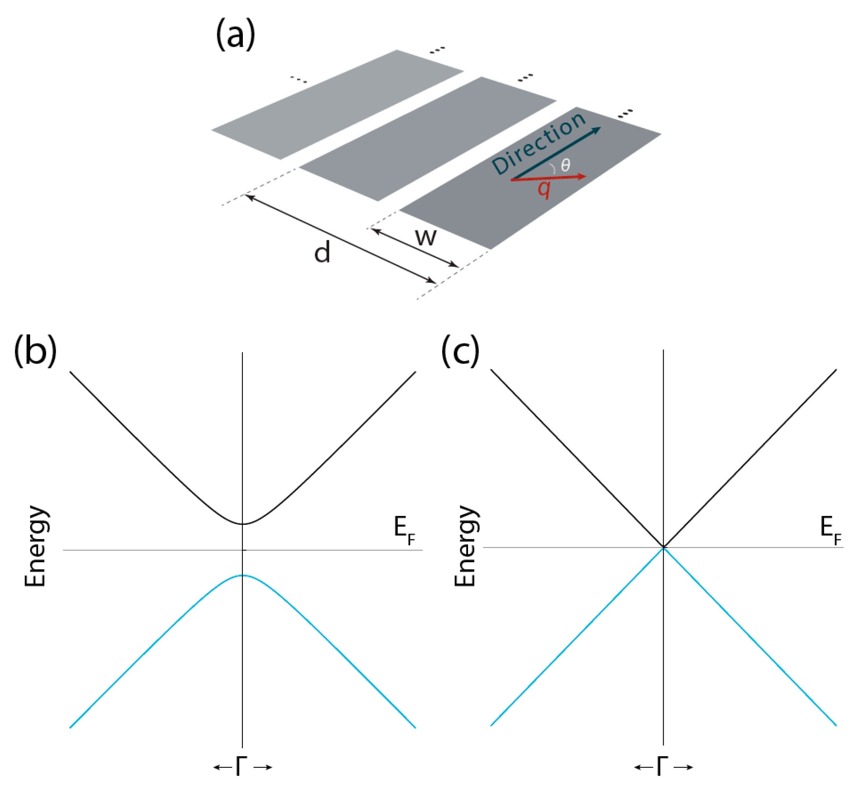
Figure 1. Schematic representations: (a) freestanding 2D GNR array; (b,c) the band dispersion around the Γ point ( k 0 ) of a hypothetical ultra-narrow and wide GNR, respectively, for n = 1 The ribbon width is denoted as w , the vacuum distance between contiguous ribbons is denoted as d w , q is the wave vector along the GNR direction, and θ is the angle for different orientations of the plasmon momentum.
Chemosensors 10 00514 g001
Figure 2. (a) Band structure and (b) density of states (DOS) of graphene computed by density functional theory (DFT). Color density plots (c,d) for the and bands in the vicinity of point vs. the charge carrier velocity, respectively. Adapted from Ref. [31].
Chemosensors 10 00514 g002
Figure 3. Bandgap (Δ) as a function of the ribbon width (w). Markers represent the GNR systems under study and the continuous line is the fitting curve using Equation (2). The numerical values of the bandgap and effective mass are calculated using two different charge carrier velocities: vF = 0.829 × 10⁶ m s−1 (blue markers) and vF = 1.0 × 10⁶ m s−1 (orange markers) and reported in Tables S2 and S3.
Chemosensors 10 00514 g003
Figure 4. Band structure and density of states (DOS) as a function of parallel component k, considering the experimental realized ribbon widths: (a) 155 nm, (b) 270 nm, (c) 380 nm, and (d) 480 nm. Blue and black curves represent the valence and conduction states, respectively.
Chemosensors 10 00514 g004
Figure 5. Plasmon frequency dispersion ( ω / 2 π ) vs. wave vector ( q ), considering different ribbons widths (155, 270, 380, and 480 nm). The parameters of Equation (4) have been fixed as: N 2 D = 1.0 × 10 12 cm−2, θ = 0 , v = 1.0 × 10¹³ s−1, and v F = 0.829 × 10 6 m s−1.
Chemosensors 10 00514 g005
Figure 6. (a) Plasmon excitation lifetime (≤4 THz) for different ribbons widths at q = 100 cm−1. (b) Plasmon excitation lifetime (≤10 THz) for different ribbons widths at q = 1000 cm−1. (c) Plasmon excitation lifetime (≤20 THz) for different ribbons widths at q = 10,000 cm−1. (d) Percentage variation in plasmon frequency by increasing ribbon width for three different q values (q = 100, 1000, 10,000 cm−1). The parameters of Equation (4) have been fixed as: N2D = 1.0 × 1012 cm−2, θ = 0, v = 1.0 × 10¹³ s−1, and vF = 0.829 × 10⁶ m s−1. The plasmon spectra were calculated using the Lorentzian line shape function to a maximum value of 1 with FWHM = 0.25.
Chemosensors 10 00514 g006
Figure 7. Plasmon frequency dispersion ( ω / 2 π ) vs. wave vector ( q ) (using N 2 D = 1.0 × 10 12 cm−2, ν = 1.0 × 10 13 s−1, and v F = 0.829 × 10 6 m s−1) for different orientations of plasmon momentum ( θ = 0 ,     60 ,     80 ) with different ribbon widths: (a) w = 155 nm, (b) w = 270 nm, (c) w = 380 nm, and (d) w = 480 nm.
Chemosensors 10 00514 g007
Figure 8. Plasmon excitation lifetime ( ω / 2 π 7 THz) (using θ = 80 , N 2 D = 1.0 × 10 12 cm−2, ν = 1.0 × 10 13 s−1, and v F = 0.829 × 10 6 m s−1) for selected q values from 1000 to 10,000 cm−1, with different ribbon widths: (a) w = 155 nm, (b) w = 270 nm, (c) w = 380 nm, and (d) w = 480 nm. The plasmon spectra were calculated using the Lorentzian shape function to a maximum value of 1 with FWHM = 0.25 .
Chemosensors 10 00514 g008
Figure 9. Plasmon excitation lifetime ( 7 THz) at (a) q = 2000 cm−1, (b) q = 5000 cm−1, (c) q = 10,000 cm−1; considering different ribbons widths (155, 270, 380, and 480 nm). (d) Percentage variation in plasmon frequency by increasing ribbon width for three different q values ( q = 2000 , 5000 , 10,000 cm−1). The parameters of Equation (4) have been fixed as: N 2 D = 1.0 × 10 12 cm−2, θ = 80 , ν = 1.0 × 10 13 s−1, and v F = 0.829 × 10 6 m s−1. The plasmon spectra were calculated using the Lorentzian shape function to a maximum value of 1 with FWHM = 0.25 .
Chemosensors 10 00514 g009
Figure 10. Plasmon frequency dispersion ( ω / 2 π ) vs. wave vector ( q ) (using θ = 0 , N 2 D = 1.0 × 10 12 cm−2, and v F = 0.829 × 10 6 m s−1) for different values of electron relaxation rate ( ν = 1.0 × 10 13 ,   2.0 × 10 13 ,   4.0 × 10 13 s−1) and different ribbon widths: (a) w = 155 nm, (b) w = 270 nm, (c) w = 380 nm, and (d) w = 480 nm.
Chemosensors 10 00514 g010
Figure 11. Plasmon excitation lifetime ( ω / 2 π 7 THz) (using θ = 0 , N 2 D = 1.0 × 10 12 cm−2, ν = 4.0 × 10 13 s−1, and v F = 0.829 × 10 6 m s−1) for selected q values from 100 to 1000 cm−1, with different ribbon widths: (a) w = 155 nm, (b) w = 270 nm, (c) w = 380 nm, and (d) w = 480 nm. The plasmon spectra were calculated using the Lorentzian shape function to a maximum value of 1 with FWHM = 0.25 .
Chemosensors 10 00514 g011
Figure 12. Plasmon excitation lifetime ( 7 THz) at (a) q = 600 cm−1, (b) q = 800 cm−1, and (c) q = 1000 cm−1 considering different ribbons widths (155, 270, 380, and 480 nm). (d) Percentage variation in plasmon frequency by increasing ribbon width for three different q values ( q = 600 , 800 , 1000 cm−1). The parameters of Equation (4) have been fixed as: N 2 D = 1.0 × 10 12 cm−2, θ = 0 , ν = 4.0 × 10 13 s−1, and v F = 0.829 × 10 6 m s−1. The plasmon spectra were calculated using the Lorentzian shape function to a maximum value of 1 with FWHM = 0.25 .
Chemosensors 10 00514 g012
Figure 13. Plasmon frequency dispersion ( ω / 2 π ) vs. wave vector ( q ) (using θ = 0 , ν = 1.0 × 10 13 s−1, and v F = 0.829 × 10 6 m s−1) for different values of charge carrier concentrations ( N 2 D = 1.0 × 10 12 ,   2.0 × 10 12 ,   4.0 × 10 12 cm−2) with different ribbon widths: (a) w = 155 nm, (b) w = 270 nm, (c) w = 380 nm, and (d) w = 480 nm.
Chemosensors 10 00514 g013
Figure 14. Plasmon excitation lifetime ( ω / 2 π 40 THz) (using θ = 0 , N 2 D = 4.0 × 10 12 cm−2, ν = 1.0 × 10 13 s−1, and v F = 0.829 × 10 6 m s−1) for selected q values from 1000 to 10,000 cm−1, with different ribbon widths: (a) w = 155 nm, (b) w = 270 nm, (c) w = 380 nm, and (d) w = 480 nm. The plasmon spectra were calculated using the Lorentzian shape function to a maximum value of 1 with FWHM = 0.25 .
Chemosensors 10 00514 g014
Figure 15. Plasmon excitation lifetime ( 40 THz) at (a) q = 1000 cm−1, (b) q = 5000 cm−1, (c) q = 10,000 cm−1; considering different ribbons widths (155, 270, 380, and 480 nm). (d) Percentage variation in plasmon frequency by increasing ribbon width for three different q values ( q = 1000 , 5000 , 10,000 cm−1). The parameters of Equation (4) have been fixed as: N 2 D = 1.0 × 10 12 cm−2, θ = 0 , ν = 4.0 × 10 13 s−1, and v F = 0.829 × 10 6 m s−1. The plasmon spectra were calculated using the Lorentzian shape function to a maximum value of 1 with FWHM = 0.25 .
Chemosensors 10 00514 g015
Figure 16. (a) Plasmon frequency dispersion ( 2 THz) ( ω / 2 π ) vs. wave vector, considering different ribbons widths (155, 270, 380, and 480 nm). The parameters of Equation (4) have been fixed as: N 2 D = 1.0 × 10 12 cm−2, θ = 0 , and ν = 0.0 s−1. (b) Plasmon excitation lifetime at 1 THz for momentum q 20 cm−1, considering different ribbons widths (155, 270, 380, and 480 nm). The plasmon spectra were calculated using the Lorentzian shape function to a maximum value of 1 with FWHM = 0.5 .
Chemosensors 10 00514 g016
Figure 17. (a) Plasmon frequency dispersion ( 2 THz) ( ω / 2 π ) vs. wave vector ( q ), considering different ribbons widths (155, 270, 380, and 480 nm). (b) Plasmon excitation lifetime for w = 155 nm, considering different momenta from 200 to 290 cm−1. The parameters of Equation (4) have been fixed as: N 2 D = 1.0 × 10 12 cm−2, θ = 0 , and ν = 2.24 × 10 13 s−1. The plasmon spectra were calculated using the Lorentzian shape function to a maximum value of 1 with FWHM = 0.5 .
Chemosensors 10 00514 g017
Figure 18. (a) Plasmon frequency dispersion ( 3 THz) ( ω / 2 π ) vs. wave vector, considering different ribbons widths (155, 270, 380, and 480 nm). The parameters of Equation (4) have been fixed as: N 2 D = 2.5 × 10 12 cm−2, θ = 0 , and ν = 2.24 s−1. (b) Plasmon excitation lifetime at 0.95 THz for momentum q 100 cm−1, considering different ribbons widths (155, 270, 380, and 480 nm). The plasmon spectra were calculated using the Lorentzian shape function to a maximum value of 1 with FWHM = 0.5 .
Chemosensors 10 00514 g018
Figure 19. (a) Plasmon frequency dispersion ( 16 THz) ( ω / 2 π ) vs. wave vector ( q ), considering different ribbons widths (155, 270, 380, and 480 nm). (b) Plasmon excitation lifetime for w = 480 nm, considering different momenta from 2000 to 3000 cm−1. The parameters of Equation (4) have been fixed as: N 2 D = 1.0 × 10 12 cm−2, θ = 0 , and ν = 2.24 × 10 13 s−1. The plasmon spectra were calculated using the Lorentzian shape function to a maximum value of 1 with FWHM = 0.5 .
Chemosensors 10 00514 g019
Publisher’s Note: MDPI stays neutral with regard to jurisdictional claims in published maps and institutional affiliations.