Article

Enhanced Electromagnetic Coupling in the Walnut-Shaped Nanostructure Array

1
School of Material and Environmental Engineering, Hangzhou Dianzi University, Hangzhou 310018, China
2
The College of Electronics and Information, Hangzhou Dianzi University, Hangzhou 310018, China
3
Shangyu Institute of Science and Engineering, Shaoxing 312000, China
4
School of Medicine, Hangzhou Dianzi University, Hangzhou 310018, China
5
College of Physical Science and Technology, Xiamen University, Xiamen 361005, China
*
Authors to whom correspondence should be addressed.
Chemosensors 2022, 10(11), 445; https://doi.org/10.3390/chemosensors10110445
Submission received: 19 September 2022 / Revised: 23 October 2022 / Accepted: 24 October 2022 / Published: 26 October 2022
(This article belongs to the Special Issue SERS Sensing Technology: Research, Progress and Applications)

Abstract

:
It is a challenging yet valuable work to prepare a surface-enhanced Raman scattering (SERS) substrate with low cost and high performance by simple methods. In this study, the Ag nanoparticles were sputtered on PS spheres by the magnetron sputtering, which was used as the mask to create the nanostructures by etching the spheres. Because of the heating effect in the etching process, the Ag nanoparticles gathered on the surfaces of PS spheres when the etching time was 60 s. Strong electromagnetic coupling was observed between the gathered Ag nanoparticles as confirmed by FDTD simulation and SERS signals from the probe molecule 4-mercaptobenzoic acid. This structure showed the detection limit for thiram down to 10−8 M.
Keywords:
SERS; nano-gap; thiram

1. Introduction

As an efficient sulfur fungicide [1], thiram is widely used in agricultural production [2,3]. The thiram easily remains on crops and accumulates in the human body due to its poor solubility [4,5]. It is difficult to eliminate thiram from the human body once absorbed, which poses a serious threat to human health [6,7]. The thiram is colorless and tasteless, which makes it difficult for the ordinary consumers to detect the thiram in the products. Several common methods for thiram detection include enzyme-linked immunosorbent assay (ELISA), chromatography-mass spectrometry (GC-MS/LC-MS) and thin layer chromatography (TLC) [8,9,10]. These methods have some shortcomings, for example, complicated operation, poor repeatability and expensive detection instruments, which makes it difficult for ordinary consumers to use the methods above without professional knowledge [11,12]. Based on these demands, researchers have proposed a convenient and simple detection method—Surface Enhanced Raman spectroscopy (SERS) [13,14].
As a detection technology with fingerprint effect and detection at the single molecule level, SERS spectrum is widely used in many fields [15,16], such as chemical substances, biomedicine, environmental detection, food safety and so on [17,18]. For the enhancement mechanism of SERS spectrum, it is generally believed that the electromagnetic enhancement coexists with the chemical enhancement [19]. In comparison with the contribution of chemical mechanism 102–103, the contribution of the electromagnetic mechanism is 103–108 [20]. The fundamental basis of electromagnetic enhancement comes from the coupled electromagnetic field provided by SERS substrate [21,22]. Based on the experimental observations and theoretical calculations, the regions composed of nanogaps and nanotips make the main contribution to the SERS enhancement, called hotspots under significant resolution, depending on the nanostructure shapes, sizes, materials and patterns [23,24,25,26]. The SERS substrate is usually made of noble metal materials such as gold and silver. In order to ensure the uniformity of the detection signal of the SERS substrate, the pattern of the prepared SERS substrate should be consistent. To achieve better detection, many effective types of nanostructures have been developed to get the significant hotspots, including nanocubes [27], nanorods [28], nanotriangles [29], nanowires [30], nano-octahedra [31], nanoflowers [32] and nanostars [33], and other structures make further efforts in improving the sharpness and roughness of the structural surfaces. Cheng et al. prepared the arrays of bridged knobby units on PS spheres arrays by co-sputtering Ag and SiO2, and the arrays of bridged knobby units is successfully applied to the early diagnosis of hepatocellular carcinoma (HCC) [34]. The surface roughness of PS spheres is improved obviously by co-sputtering. Zhu et al. prepared Au nanocone arrays based on nanosphere lithography, the sharpness of the Au nanocone is affected by changing the sputtering angle [35].
To get the uniform hotspots distribution at defined locations, the ordered nanostructures arrays are prepared by some techniques, including lithography, nanosphere lithography and electron beam lithography. Once the patterned array forms, it is challenging to change the hotspots’ density and distribution. In this study, the film composed of Ag nanoparticles is deposited onto PS array and the walnut-shaped nanostructures are obtained by ion etching PS spheres into the columnar structure, with Ag nanoparticles as the mask. The long etching time makes the etched columnar structure collapse due to the heating effect [36], which gathers the metal nanoparticles. The gathered Ag nanoparticles make the PS array like a walnut, which evinces the strong electromagnetic coupling in the gathered nanostructures suitable for SERS substrate, as approved by the probe molecule 4-MBA and the simulation based on FDTD. This SERS substrate is successfully used to detect thiram in the concentrations down to 10−8 M.

2. Experiment

2.1. Experimental Materials

Polystyrene spheres (PS) with an average particle size of 500 nm (concentration 10 wt% and a density 1.05 g/cm3) were purchased from Huake Micro Technology Co., Ltd., Wuhan, China. Silicon wafers were purchased from Kejing Co., Ltd., Hefei, China. Thiram was purchased from Alta Technology Co., Ltd., Tianjin, China. Sodium dodecyl sulfate was purchased from Sinopharm Chemical Reagent Co., Ltd., Beijing, China. 4-mercaptobenzoic acid (4-MBA) was purchased from Budweiser Technology Co., Ltd., Tianjin China. NH3·H2O (25%), H2O2 (30%) and ethanol (AR) were purchased from Aladdin Biochemical Technology Co., Ltd., Shanghai, China. Ag and SiO2 targets (99.999%) were obtained from Beijing TIANQI Advanced Materials Co., Ltd. Ultrapure water (18.2 MΩ.cm) was supplied by ultrapure water machine (GREEN-Q2-10T, EPED, Nanjing, China.). All experiments were conducted at room temperature and in a dry and dust-free environment.

2.2. Preparation of the Two-Dimensional 500 nm PS Spheres Array

Firstly, the silicon wafer needs to be cleaned to remove impurities on its surface. Immerse the silicon wafer (size 2 cm × 2 cm) in the mixed solution of NH3·H2O, H2O2 and H2O, NH3·H2O, H2O2, H2O, mixed at a volume ratio of 2:1:6, heat the mixed solution until bubbling and continue until no bubbling occurs. Wait for the temperature of the waste liquid to drop to room temperature, and wash the silicon wafer with ultrapure water to remove the residual waste liquid. Ultrasonic cleaning is performed with alcohol for 3 cycles, the duration of ultrasonic treatment on silicon wafer is 15 min. In order to preserve the cleaned silicon wafers, it is necessary to put the silicon wafers into ultrapure water to avoid contacting the dust in the air. Secondly, 650 μL ultrapure water and 325 μL ethanol are mixed with 150 μL monodisperse polystyrene colloidal sphere solution. Transfer the mixed solution into a 1 mL centrifuge tube with a pipette gun, place the centrifuge tube in the ultrasonic cleaning machine for 5 min so that the PS spheres are evenly dispersed in the mixed solution. Then, the cleaned silicon wafer is placed at the bottom of the 10 cm culture dish; transfer the mixed solution from the centrifuge tube to a 1 mL injection syringe, while the injection syringe equipped with a PS spheres solution is fixed to the syringe pump. By adjusting the injection rate of the syringe pump, each drop of PS spheres solution is uniformly dispersed on the water surface. The PS spheres will be self-assembled into a mono-layer PS spheres film in the culture dish. When a mono-layer PS spheres film of sufficient size is formed on the water surface, turn off the syringe pump. A pipette gun is used to drop 50 μL of the sodium dodecyl sulfate into the culture dish to stabilize the nanospheres. Subsequently, the peristaltic pump is used to replace the water in the culture dish at a rate of 80 mL/min to remove the excess PS spheres below the liquid level. Finally, the excess water in the culture dish is removed at a rate of 20 mL/min until the mono-layer PS spheres film is deposited on the silicon wafer. When the moisture in the silicon wafer is completely evaporated, the sample is placed in a room temperature and dry environment for use. Thus, the mono-layer PS spheres film on silicon wafer is obtained.

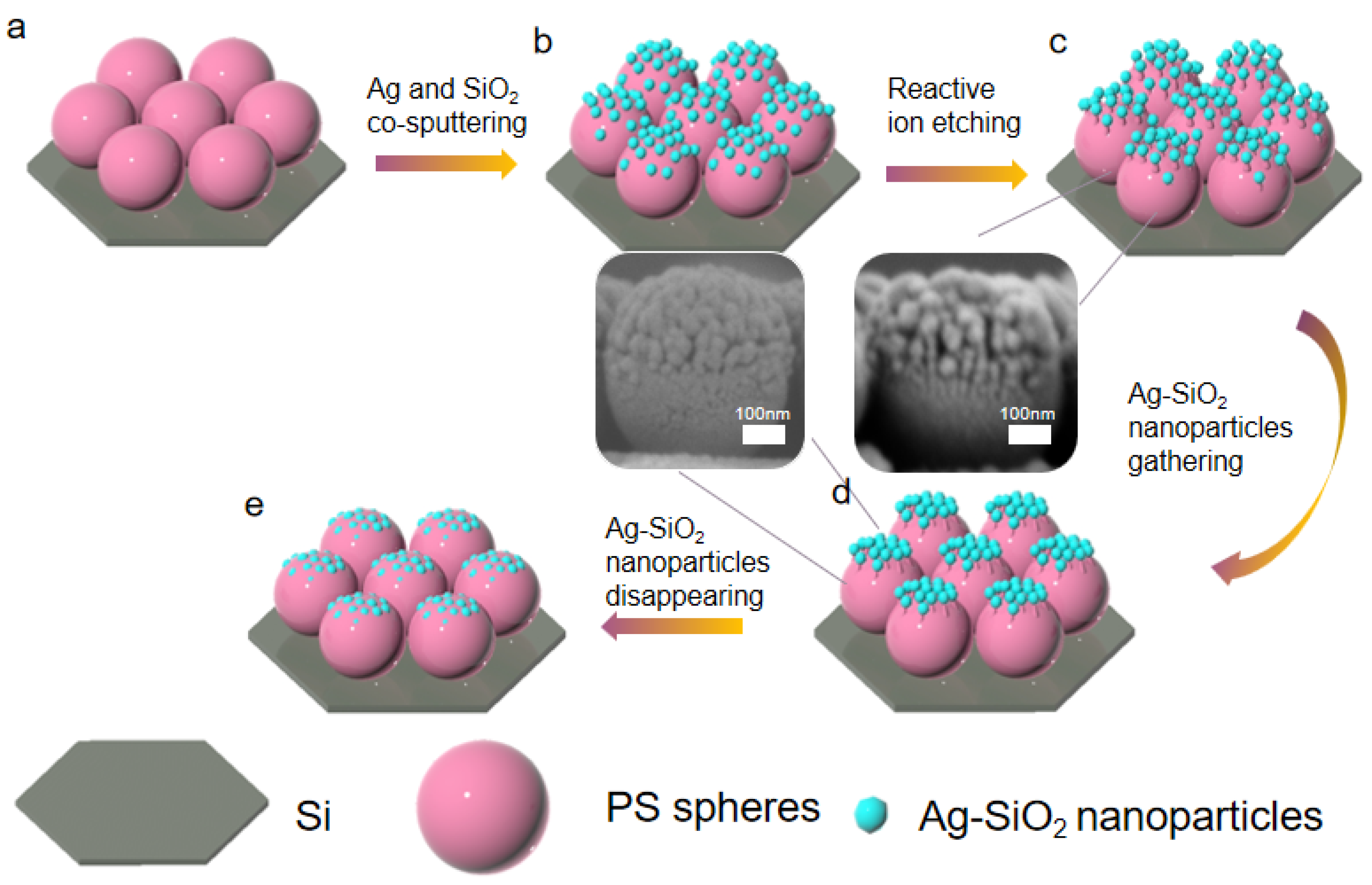
2.3. Preparation of the Walnut-Shaped Nanostructure Array

The magnetron sputtering system (FJL-700, Shenkeyi, China) is used to prepare the sample by co-sputtering Ag by direct current (DC) target and SiO2 by radio frequency (RF) target onto two-dimensional (2D) PS sphere arrays. The argon flux during sputtering is 25 SCCM and the working pressure is 1.2 Pa, while the background pressure is 2 × 10⁻⁴ Pa. The power of sputtering Ag is set up as 10 W, the power of sputtering SiO2 is set up as 40 W, and the co-sputtering time is 10 s, 20 s, 30 s. Then, the sputtered mono-layer PS spheres film is processed by ion etching. Place the sample to be etched on a complete silicon wafer and place the complete silicon wafer in the central area of the reactive ion etching machine to ensure the uniformity of the sample. The oxygen flux is 50 sccm, the working pressure is 20 Pa, the background pressure is 1 × 10⁻³ Pa and the etching power is 150 W. The sputtered mono-layer PS spheres film is etched for 0 s, 30 s, 60 s and 90 s, respectively.

2.4. FDTD Simulations

The electromagnetic field distribution in the prepared nanostructure was simulated by FDTD (Finite Difference Time Domain) software. The software manufacturer was ANSYS and the software version was 8.19.1584. The calculation in FDTD software is based on the Maxwell equation. The algorithm of the FDTD has the advantages of wide application range and high precision. The substrate is placed on the X-Y plane. In the x-axis and y-axis directions, the boundary conditions of FDTD is set to periodic. The boundary conditions of FDTD is set to the perfectly matched layer (PML) in the z-axis. The X-Z plane monitor is placed on the middle of adjacent PS spheres to monitor the electric field intensity. The simulation time of FDTD is 1000 fs and the simulation temperature of FDTD is 298 k (room temperature). The dielectric constant and permeability values of Ag and SiO2 given by FDTD software are chosen for the simulation. The background index of FDTD is set as 1 and the refractive index of the PS spheres is set as 1.585. The mesh type is uniform and the mesh accuracy is set as 8, the minimum mesh step is set as 0.25 nm. The minimum value of automatic turn-off is set to 1 × 10⁻⁵. The planar wave incident light source is placed 400 nm above the nanostructure, the wavelength range of the planar wave incident light source is set at 400 to 800 nm. The radius of PS sphere and the radius of Ag-SiO2 nanoparticles, and the spaces between nanoparticles are obtained from SEM images.

2.5. Characterization of Structure and Surface-Enhanced Raman Scattering

SEM was performed on a field emission scanning electron microscopy (15 kV, JEOL 7800F); the working voltage set to 5 kV. The AFM is NanoWizard 4-NanoScience, Germany, JPK Instrument AG, and the scanning mode is QI topography scanning and the scanning frequency is 250 μm/s. AFM probe is PPP-FMAuD-10 NANOSENSORS (n*-silicon, the resistivity 0.01~0.02 Ωcm, the force constant 0.5~9.5 N/m). Tip radius is 3.0 ± 1 μm (thickness), 225 ± 10 μm (length), 28 ± 10 μm (width). AFM is used to observe the morphology of the sample and obtain the rates of Ag and SiO2 deposition. As shown in Figure S1, the Ag sputtering rate was 0.83 nm/s and the SiO2 sputtering rate was 0.0933 nm/s. The etching system is reactive ion etching (RIE-10NR Japan). High-resolution transmission electron microscopic (HRTEM) model number is Talos F200S (Thermo Fisher Scientific, America). SERS spectra are measured by Ruhai Raman system, the laser wavelength is 785 nm and the diameter of the laser spot focused by the microscope is 2 μm. The working power is set to 100 mW and the integration time is set to 1000 ms, measure for 5 times and take the average value. Use clean silicon wafer for calibration before measuring the sample. After calibration, the silicon wafer peak is accurately positioned at 520 cm−1.

2.6. Thiram Detection

The SERS substrates are immersed in the thiram solution with the concentration of 10−6 M, 10−7 M, 10−8 M, 10−9 M, for an hour. After the immersion, the samples are rinsed with absolute ethanol in order to remove free or physically adsorbed excess probe molecules on the surface of the structure.

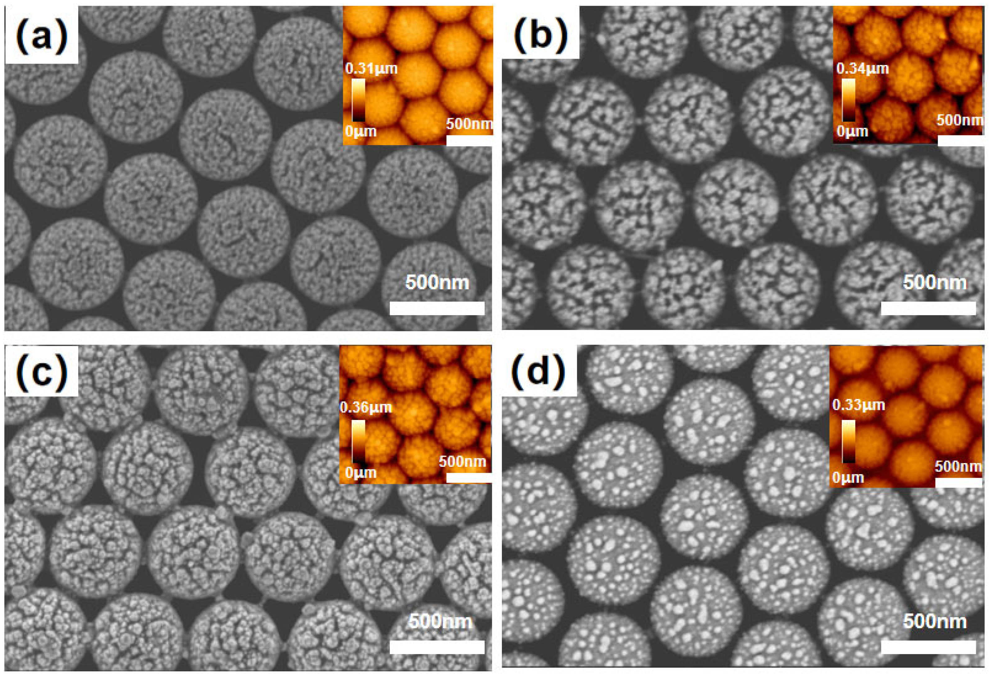
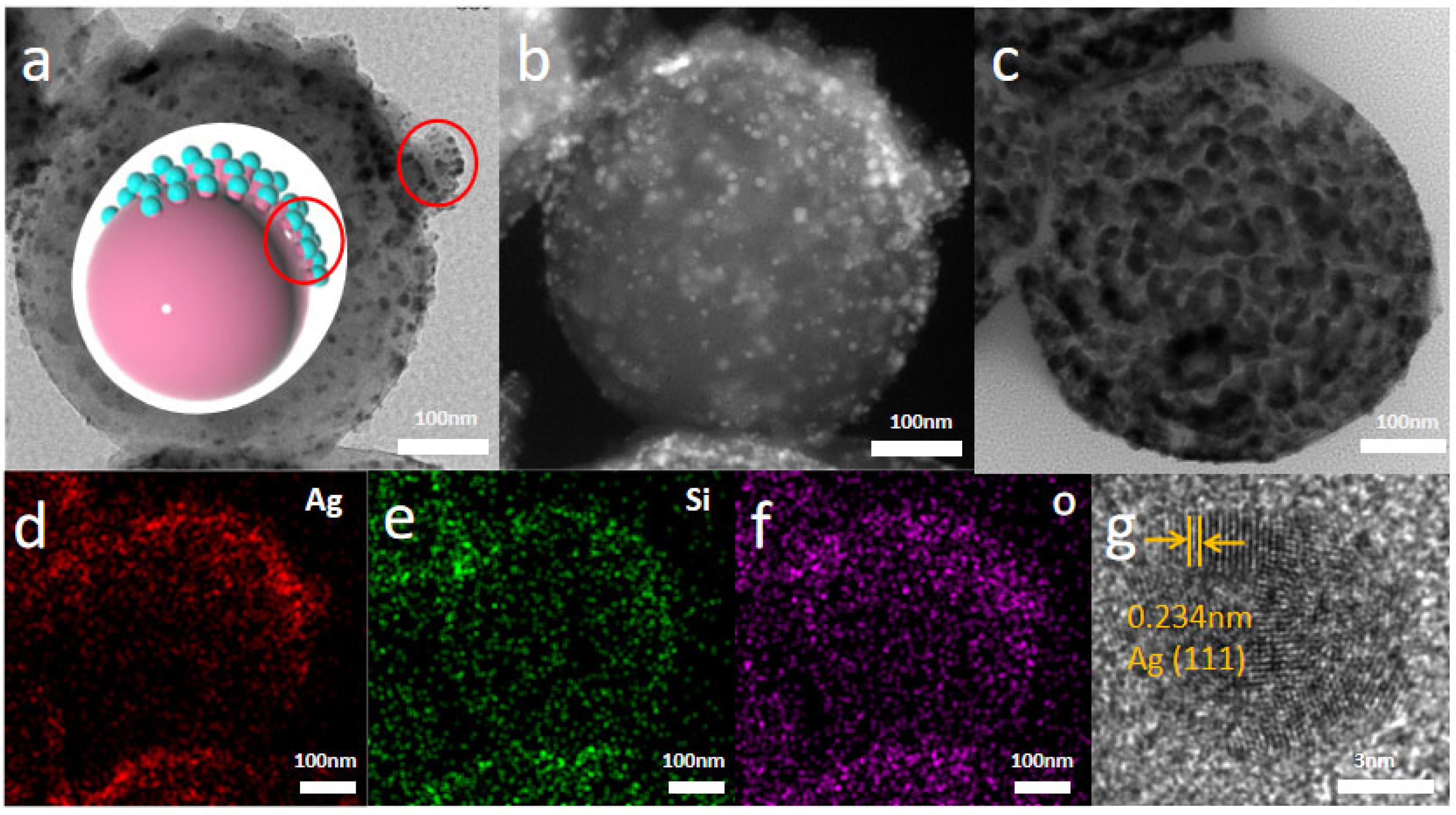
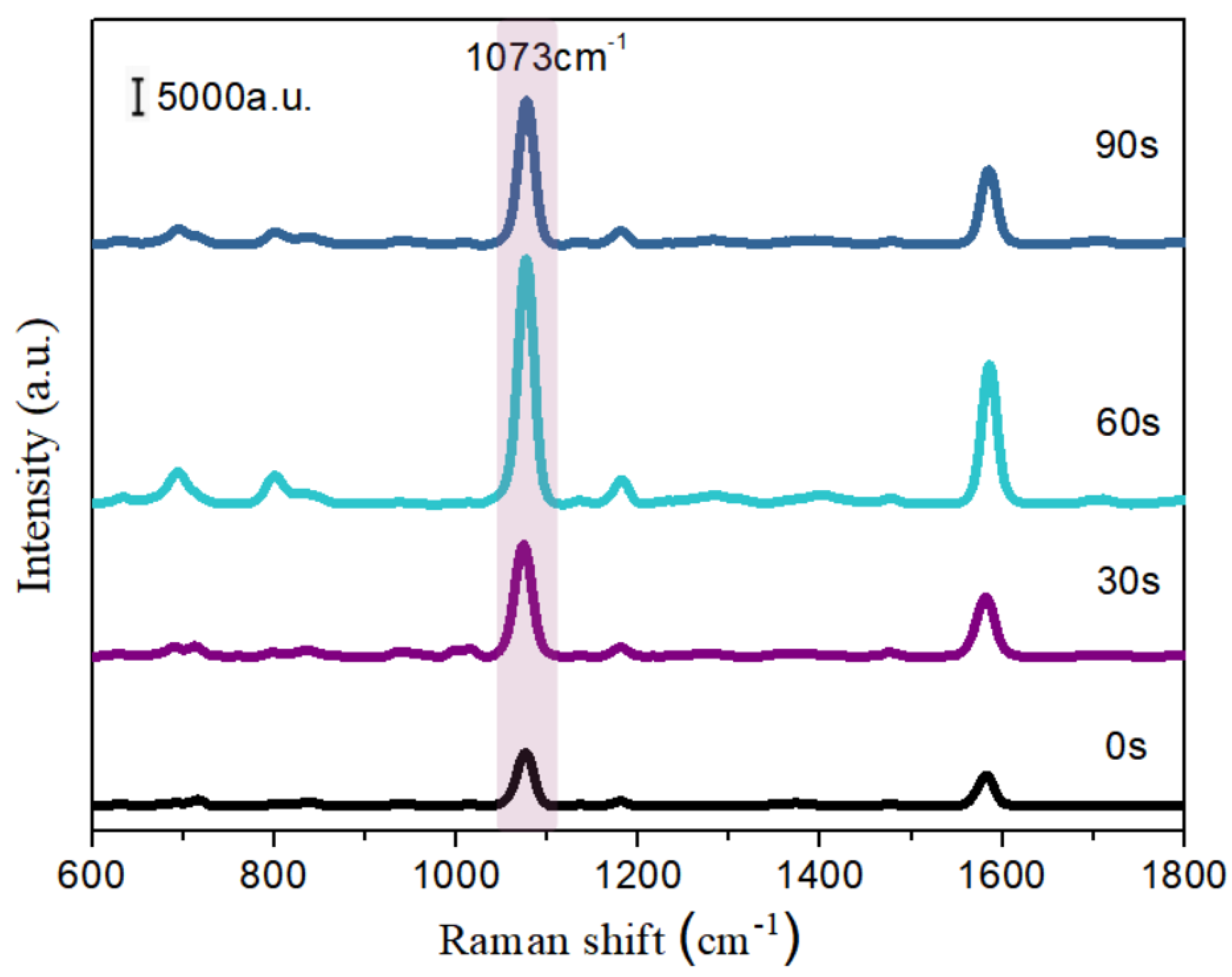
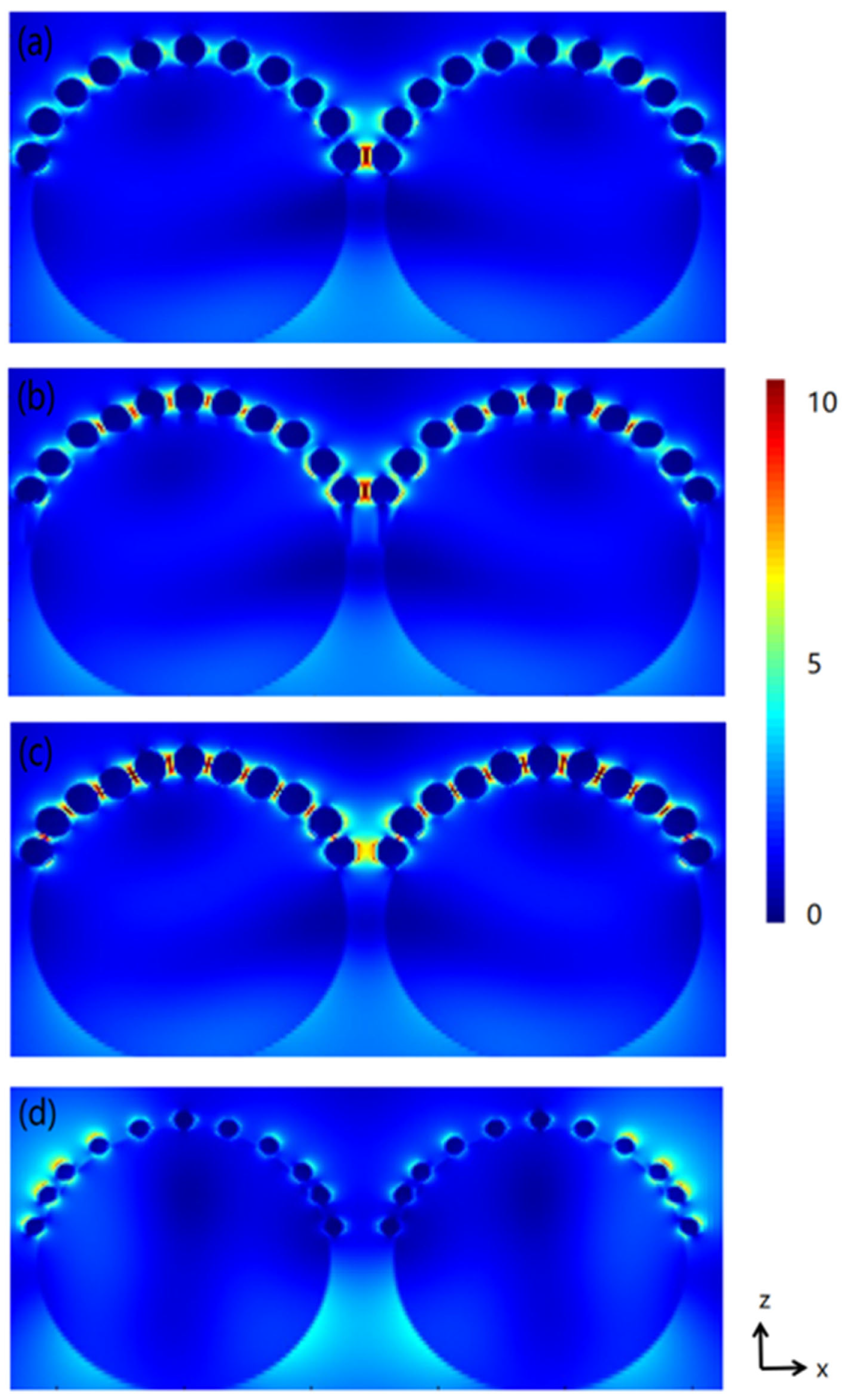
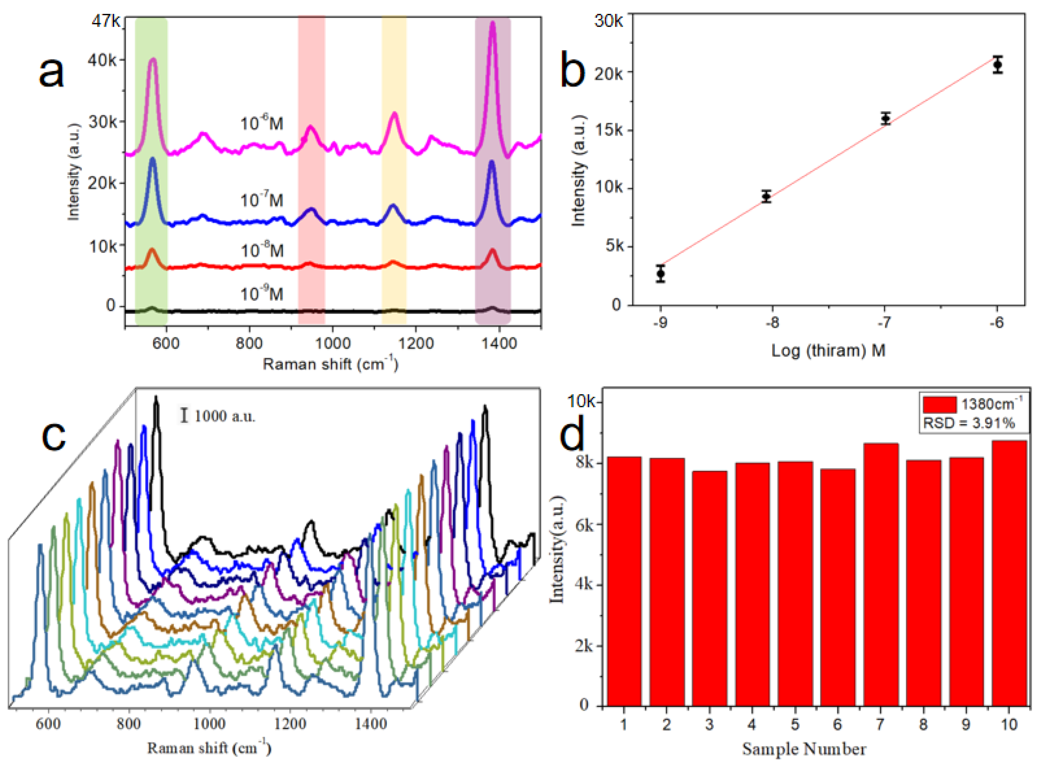
3. Results and Discussion

Based on two-dimensional 500 nm PS arrays by self-assembly on Si substrate, the walnut-shaped nanostructure for the particle film with Ag isolated by SiO2 is fabricated and the detailed procedure is illustrated in Figure 1. First, PS array with the size 500 nm is self-assembled on Si substrate, forming the two-dimensional close compact structure. Second, Ag and SiO2 film with different thickness are co-sputtered onto PS spheres arrays by magnetron sputtering. Third, the PS array with Ag-SiO2 film is etched by oxygen ion for different times to get the walnut-shaped nanostructures.
Figure 2 shows the SEM images of 10 nm Ag-SiO2 nanoparticle film with etching time. When the ion etching is applied to the PS sphere covered by the particles film, the surface of sample shows different morphology features with etching time. The Ag-SiO2 nanoparticles on PS surface begin to gradually shrink and gather with etching time, and the distances between particles become 20 nm, which transforms the film into the walnut-shaped nanostructures for etching time 30 s and 60 s. Ag-SiO2 nanoparticles are located on the top of the PS spheres. When ion etching is applied to the substrate, the Ag-SiO2 nanoparticles on PS spheres is etched much slowly in comparison to PS around particles, which indicates the Ag-SiO2 nanoparticles serve as the mask during etching as shown in the section-view SEM image. During the etching process, the heating effect during the etching process softens the PS posts, which deforms the PS posts and causes the nanoparticles to bind together, similar to the observations by some researchers [37]. When the etching time is prolonged to 90 s, the Ag nanoparticles are clearly etched. The Ag-SiO2 nanoparticles show the uniform distribution and separation from each other. Figures S2 and S3 give the SEM images of 20 nm and 30 nm Ag-SiO2 nanoparticle film with different etching times. Before the etching, the nanoparticles are separated. As shown in Figures S1b and S2b, Ag-SiO2 nanoparticles are located on the tops of PS columnar structures. When the ion etching is applied to the PS sphere, both samples show the aggregated Ag nanoparticles due to the heating effects.
Figure 3a shows the TEM image of the sample 10 nm Ag-SiO2 film after etching 30 s. The PS columnar structures are observed on the surface of spheres with the lateral sizes around 40 nm as shown by the red circle. The detailed analysis shows the columnar structures are composed of many smaller ones and the lateral size is 10 nm, which is in agreement with the size of the Ag nanoparticles, as shown in Figure 3b. The element mapping images confirm the existences of Ag, Si and O in the samples (Figure 3d–f). The HRTEM image shows Ag nanoparticles surrounded by amorphous SiO2 forming Ag@SiO2 core-shell structure. Figure 3g shows the lattice plane is 0.234 nm and the lattice agrees with Ag (111), which indicates the Ag is free of oxidation due to the protection by SiO2.
Figure 4 shows the SERS characterization of samples excited by 785 nm laser after immersion in the 4-MBA solution 10−3 M for 1 h. After the immersion, the samples were rinsed with absolute ethanol in order to remove free or physically adsorbed excess probe molecules on the surface of the structure, and the samples were dried with nitrogen gas and put into a dry dust-free environment for later use. Two obvious Raman peaks are observed at 1073 cm−1 and 1575 cm−1. The peak at 1073 cm−1 is attributed to aromatic ring breathing, symmetric C-H in-plane bending and C-S stretching. The peak at 1575 cm−1 belongs to ring C-C stretch and asymmetric C-H in-plane bending. The peaks are selected to compare the electromagnetic coupling of different SERS substrates. There are some weak characteristic peaks, the peak at 719 cm−1 is attributed to γ (CCC) out-of-plane ring vibration and the peak at 846 cm−1 belongs to δ (COO−) bending vibration. The intensity of the characteristic peak at 1073 cm−1 increases with the etching time from 30 s to 60 s, and then decreases for the etching time 90 s. The intensity increase of characteristic peaks can be attributed to the strong plasmon coupling between the walnut-shaped nanostructure when the Ag-SiO2 nanoparticles gather due to the softened PS posts. When the etching time exceeds 60 s, for example 90 s, the intensity decreases again, which is due to the increased distances between Ag-SiO2 nanoparticles by etching.
FDTD simulation is used to show the evolution of the electromagnetic field among the walnut-shaped nanostructures, as shown in Figure 5. When the etching time is short, the radius of the PS spheres shows no obvious changes. Therefore, the radius of PS sphere is set as 250 nm for all simulations. To show the effects of the Ag nanoparticle aggregation on the electromagnetic couplings in the walnut-shaped nanostructures, the distributions of the electromagnetic fields were simulated for the different spaces between Ag nanoparticles. Ag nanoparticle size was chosen as 25 nm. The spaces between the Ag nanoparticles were set as 25 nm, 20 nm, 15 nm, corresponding to the different etching time 0 s, 30 s and 60 s. For the sample etched for 90 s, the Ag nanoparticle size is decreased responsible for the space increase to 17 nm. When the sample is not etched, the electromagnetic coupling is observed between Ag-SiO2 particles on the PS spheres (Figure 5a). For the etched samples, the electromagnetic coupling is enhanced due to the formation of the walnut-shaped nanostructures and the enhancement is maximum for 60 s (Figure 5b,c). When the etching time increases to 60 s, the electromagnetic coupling between the Ag nanoparticles increases (Figure 5c). In comparison to the contribution of Ag nanoparticles, the simulation results show that the hotspots are mainly distributing in the nanogaps of the walnut-shaped nanostructures due to the unique geometric characteristics. In addition, the relatively uniform distribution of nanogaps indicates the ability to capture the probe molecule, which is consistent with the results of SERS. When the etching time reaches 90 s, the hotspots on the surface of PS spheres are significantly decreased because the reduced sizes of Ag nanoparticles and the increased distances between Ag nanoparticles, which leads to the reduced SERS intensity.
To analyze enhancement factor (EF), the 4-MBA signals of the presence and absence of SERS substrates are compared. The formula is used to analyze enhancement factor, EF = (ISERS/NSERS)/(INR/NNR). ISERS and INR are the SERS intensity detected on SERS substrate and the Raman characteristic peak intensity of pure 4-MBA powder, respectively. NSERS is the amount of 4-MBA adsorbed on SERS substrate and NNR is the amount of 4-MBA irradiated by laser spot. In the experiment, NSERS = NdAlaserAN/σ, where σ is the area occupied by a probe molecule (0.33 nm2), Nd is the number density of colloidal spheres and AN is the hemispherical surface area of colloidal spheres. NNR = ρAlaserhNA/M, Alaser is the area of the laser spot (4 μm2), ρ is the density of solid 4-MBA (1.5 g/cm3), M is the molecular weight of 4-MBA (154.19 g/mol), and h is the effective depth of laser (20 μm). ISERS/INR is calculated as 1.7 × 10² and NNR/NSERS is calculated as 1.11 × 10⁵. The EF of the nanostructure is 1.9 × 10⁷.
The walnut-shaped sample after 60 s etching is chosen as SERS substrate to detect the thiram with different concentrations. Figure 6 shows the Raman spectra for the different concentrations of thiram. The thiram SERS peaks are successfully detected even for the concentration 10−8 M. The SERS spectrum of thiram shows the strongest peak and the second strongest peak at 1380 cm−1 and 560 cm−1, respectively. The peak at 1380 cm−1 is attributed to CN stretching and CH3 symmetry, and the peak at 560 cm−1 belongs to C-S-S asymmetric stretching vibration. The peak at 930 cm−1 is attributed to C=S stretching and CH3N, and the peak at 1138 cm−1 belongs to CN stretching and CH3 rocking modes. The intensities of the characteristic peak decrease when the thiram concentrations decrease. The SERS substrate successfully detects thiram with the concentration of 10−8 M, which is well below the minimum concentration set by the U.S. Environmental Protection Agency. We calculate the function between the intensity of characteristic peak at 1380 cm−1 and the logarithm of extract concentration, obtaining the relationship between the intensity of Raman peak and the concentration of thiram, as shown in Figure 6b. The relationship between x and y conforms to the fitting equation y = 10,486 logx + 30215, R2 = 0.976. indicating the perfect linear dependence of the logarithm of the thiram concentrations on the changed intensity of the SERS peak at 1380 cm−1. When the logarithmic concentration is lower than 10−8 M, the average peak intensity at 1380 cm−1 deviates from the linear. The lowest concentration that can be determined to be statistically different from a blank is considered as the limit of detection of the sensor [38,39,40]. This structure shows the detection limit for thiram down to 10−8 M. In practical applications, SERS substrates are required to have high uniformity in addition to high sensitivity, which should be considered. Figure 6c shows the almost identical Raman signals from 10 random points overall the sample. For better display, the intensity of the characteristic peak at 1380 cm−1 is selected to make a columnar chart, and the relative standard deviation of 10 points is calculated to be 3.91%.

4. Conclusions

In this work, we prepared a SERS substrate composed of Ag nanoparticles based on PS array by co-sputtering Ag and SiO2. The ion etching increased the plasma coupling between Ag nanoparticles because the etching process decreased the distances between Ag nanoparticles by softening the PS columnar structures. Due to the strong electromagnetic coupling effects at the nano-gap between the Ag-SiO2 nanoparticles, the SERS substrate demonstrated a high sensitivity and excellent reliability for the thiram detection with a detection limit as low as 10−8 M.

Supplementary Materials

The following are available online at https://www.mdpi.com/article/10.3390/chemosensors10110445/s1, Figure S1: AFM of the Ag film and SiO2 film; Figure S2: SEM of the nanostructure with the Ag-SiO2 nanoparticle film (20 nm) after etching for (a) 0 s, (b) 30 s, (c) 60 s, (d) 90 s; Figure S3: SEM of the nanostructure with the Ag-SiO2 nanoparticle film (30 nm) after etching for (a) 0 s, (b) 30 s, (c) 60 s, (d) 90 s. Figure S4: SERS spectra for thiram detection with different concentrations and thiram-free solution.

Author Contributions

D.M. and X.Z. contributed equally to this work. D.M. contributed to conceptualization, software, visualization, formal analysis and writing-original draft preparation. X.Z. contributed to conceptualization, methodology and writing-review and editing. J.W. contributed to validation, resources, project administration and supervision. A.W. contributed to investigation. R.G. contributed to data curation. Y.W. contributed to validation, resources, project administration and supervision. All authors have read and agreed to the published version of the manuscript.

Funding

This work is supported by the National Natural Science Foundation of China (Nos. 51901060, 12004090); the National Natural Science Foundation of Zhejiang Province (Nos. LY21E010004, LQ21A040009); the Fundamental Research Funds for the Provincial Universities of Zhejiang (No. GK209907299001–025).

Institutional Review Board Statement

Not applicable.

Informed Consent Statement

Informed consent was obtained from all subjects involved in the study.

Data Availability Statement

This study did not report any data.

Conflicts of Interest

The authors declare no conflict of interest.

References

  1. Liu, J.; Si, T.; Zhang, L.; Zhang, Z. Mussel-inspired fabrication of SERS swabs for highly sensitive and conformal rapid detection of thiram bactericides. Nanomaterials 2019, 9, 1331. [Google Scholar] [CrossRef] [PubMed] [Green Version]
  2. Kim, D.; Kim, J.; Henzie, J.; Ko, Y.; Lim, H.; Kwon, G.; You, J. Mesoporous Au films assembled on flexible cellulose nanopaper as high-performance SERS substrates. Chem. Eng. J. 2021, 419, 129445. [Google Scholar] [CrossRef]
  3. Yao, C.; Gao, X.; Liu, X.; Shen, Y.; Xie, A. In-situ preparation of ferrero chocolate-like Cu2O@Ag microsphere as SERS substrate for detection of thiram. J. Mater. Res. Technol. 2021, 11, 857–865. [Google Scholar] [CrossRef]
  4. Wang, Q.; Wu, D.; Chen, Z. Ag dendritic nanostructures for rapid detection of thiram based on surface-enhanced Raman scattering. RSC Adv. 2015, 5, 70553–70557. [Google Scholar] [CrossRef]
  5. Kim, D.; Gwon, G.; Lee, G.; Jeon, Y.; Kim, U.J.; Alothman, Z.A.; You, J. Surface-enhanced Raman scattering-active AuNR array cellulose films for multi-hazard detection. J. Hazard. Mater. 2021, 402, 123505. [Google Scholar] [CrossRef]
  6. Plou, J.; García, I.; Charconnet, M.; Astobiza, I.; García-Astrain, C.; Matricardi, C.; Liz-Marzán, L.M. Multiplex SERS detection of metabolic alterations in tumor extracellular media. Adv. Funct. Mater. 2020, 30, 1910335. [Google Scholar] [CrossRef]
  7. Sun, Y.; Xu, L.; Zhang, F.; Song, Z.; Hu, Y.; Ji, Y.; Yang, H. A promising magnetic SERS immunosensor for sensitive detection of avian influenza virus. Biosens. Bioelectron. 2017, 89, 906–912. [Google Scholar] [CrossRef]
  8. Asgari, S.; Sun, L.; Lin, J.; Weng, Z.; Wu, G.; Zhang, Y.; Lin, M. Nanofibrillar cellulose/Au@Ag nanoparticle nanocomposite as a SERS substrate for detection of paraquat and thiram in lettuce. Microchim. Acta 2020, 187, 390–403. [Google Scholar] [CrossRef]
  9. Quan, Y.; Yao, J.; Yang, S.; Chen, L.; Liu, Y.; Lang, J.; Gao, M. Detect, remove and re-use: Sensing and degradation pesticides via 3D tilted ZMRs/Ag arrays. J. Hazard. Mater. 2020, 391, 122222. [Google Scholar] [CrossRef]
  10. Tegegne, W.A.; Su, W.N.; Tsai, M.C.; Beyene, A.B.; Hwang, B.J. Ag nanocubes decorated 1T-MoS2 nanosheets SERS substrate for reliable and ultrasensitive detection of pesticides. Appl. Mater. Today 2021, 21, 100871. [Google Scholar] [CrossRef]
  11. Huo, D.; Chen, B.; Meng, G.; Huang, Z.; Li, M.; Lei, Y. Ag-nanoparticles@bacterial nanocellulose as a 3D flexible and robust surface-enhanced Raman scattering substrate. ACS Appl. Mater. Interfaces 2020, 12, 50713–50720. [Google Scholar] [CrossRef] [PubMed]
  12. Zhao, X.; Wen, J.; Zhu, A.; Cheng, M.; Zhu, Q.; Zhang, X.; Zhang, Y. Manipulation and applications of hotspots in nanostructured surfaces and thin films. Nanomaterials 2020, 10, 1667. [Google Scholar] [CrossRef] [PubMed]
  13. Zhu, A.; Zhao, X.; Cheng, M.; Chen, L.; Wang, Y.; Zhang, X.; Zhang, X. Nanohoneycomb surface-enhanced Raman spectroscopy-active chip for the determination of biomarkers of hepatocellular carcinoma. ACS Appl. Mater. Interfaces 2019, 11, 44617–44623. [Google Scholar] [CrossRef] [PubMed]
  14. Huang, Z.; Zhang, R.; Chen, H.; Weng, W.; Lin, Q.; Deng, D.; Kong, J. Sensitive polydopamine bi-functionalized SERS immunoassay for microalbuminuria detection. Biosens. Bioelectron. 2019, 142, 111542. [Google Scholar] [CrossRef] [PubMed]
  15. Langer, J.; Jimenez, D.; Aizpurua, J.; Alvarez-Puebla, R.A.; Auguie, B.; Baumberg, J.J.; Liz-Marzan, L.M. Present and future of surface-enhanced Raman scattering. ACS Nano 2020, 14, 28–117. [Google Scholar] [CrossRef] [Green Version]
  16. Zhang, P.; Zhou, X.; He, M.; Shang, Y.; Tetlow, A.L.; Godwin, A.K.; Zeng, Y. Ultrasensitive detection of circulating exosomes with a 3D-nanopatterned microfluidic chip. Nat. Biomed. Eng. 2019, 3, 438–445. [Google Scholar] [CrossRef]
  17. Xu, K.; Zhou, R.; Takei, K.; Hong, M. Toward flexible surface-enhanced Raman scattering (SERS) sensors for point-of-care diagnostics. Adv. Sci. 2019, 6, 1900925. [Google Scholar] [CrossRef]
  18. He, X.; Yang, S.; Xu, T.; Song, Y.; Zhang, X. Microdroplet-captured tapes for rapid sampling and SERS detection of food contaminants. Biosens. Bioelectron. 2020, 152, 112013. [Google Scholar] [CrossRef]
  19. Liu, Y.; Ma, H.; Han, X.X.; Zhao, B. Metal-semiconductor heterostructures for surface-enhanced Raman scattering: Synergistic contribution of plasmons and charge transfer. Mater. Horiz. 2021, 8, 370–382. [Google Scholar] [CrossRef]
  20. Lee, H.K.; Lee, Y.H.; Koh, C.S.L.; Phan-Quang, G.C.; Han, X.; Lay, C.L.; Ling, X.Y. Designing surface-enhanced Raman scattering (SERS) platforms beyond hotspot engineering: Emerging opportunities in analyte manipulations and hybrid materials. Chem. Soc. Rev. 2019, 48, 731–756. [Google Scholar] [CrossRef]
  21. Zhu, A.; Zhang, F.; Gao, R.; Zhao, X.; Chen, L.; Zhang, Y.; Wang, Y. Increasing polarization-dependent SERS effects by optimizing the axial symmetry of plasmonic nanostructures. Appl. Surf. Sci. 2019, 494, 87–93. [Google Scholar] [CrossRef]
  22. Liu, X.; Ma, J.; Jiang, P.; Shen, J.; Wang, R.; Wang, Y.; Tu, G. Large-scale flexible surface-enhanced Raman scattering (SERS) sensors with high stability and signal homogeneity. ACS Appl. Mater. Interfaces 2020, 12, 45332–45341. [Google Scholar] [CrossRef]
  23. Ding, S.Y.; Yi, J.; Li, J.F.; Ren, B.; Wu, D.Y.; Panneerselvam, R.; Tian, Z.Q. Nanostructure-based plasmon-enhanced Raman spectroscopy for surface analysis of materials. Nat. Rev. Mater. 2016, 1, 16021. [Google Scholar] [CrossRef]
  24. Kasani, S.; Curtin, K.; Wu, N. A review of 2D and 3D plasmonic nanostructure array patterns: Fabrication, light management and sensing applications. Nanophotonics 2019, 8, 2065–2089. [Google Scholar] [CrossRef]
  25. Fu, Z.; Shen, Z.; Fan, Q.; Hao, S.; Wang, Y.; Liu, X.; Yang, Z. Preparation of multi-functional magnetic-plasmonic nanocomposite for adsorption and detection of thiram using SERS. J. Hazard. Mater. 2020, 392, 122356. [Google Scholar] [CrossRef]
  26. Agrawal, A.; Cho, S.H.; Zandi, O.; Ghosh, S.; Johns, R.W.; Milliron, D.J. Localized surface plasmon resonance in semiconductor nanocrystals. Chem. Rev. 2018, 118, 3121–3207. [Google Scholar] [CrossRef]
  27. Niu, R.; Song, C.; Gao, F.; Fang, W.; Jiang, X.; Ren, S.; Zhu, D.; Su, S.; Chao, J.; Chen, S.; et al. DNA origami-based nanoprinting for the assembly of plasmonic nanostructures with single-molecule surface-enhanced Raman scattering. Angew. Chem. Int. Ed. 2021, 60, 11695–11701. [Google Scholar] [CrossRef]
  28. Pissuwan, D.; Hattori, Y. Detection of adhesion molecules on inflamed macrophages at early-stage using SERS probe gold nanorods. Nano-Micro Lett. 2017, 9, 8–17. [Google Scholar] [CrossRef] [Green Version]
  29. Wang, M.; Krasnok, A.; Zhang, T.; Scarabelli, L.; Liu, H.; Wu, Z.; Zheng, Y. Tunable fano resonance and plasmon-exciton coupling in single Au nanotriangles on monolayer WS2 at room temperature. Adv. Mater. 2018, 30, 1705779. [Google Scholar] [CrossRef]
  30. Eom, G.; Kim, H.; Hwang, A.; Son, H.Y.; Choi, Y.; Moon, J.; Kim, B. Nanogap-rich Au nanowire SERS sensor for ultrasensitive telomerase activity detection: Application to gastric and breast cancer tissues diagnosis. Adv. Funct. Mater. 2017, 27, 11701832. [Google Scholar] [CrossRef]
  31. Xie, D.; Ma, Y.; Gu, Y.; Zhou, H.; Zhang, H.; Wang, G.; Zhao, H. Bifunctional NH2-MIL-88(Fe) metal-organic framework nanooctahedra for highly sensitive detection and efficient removal of arsenate in aqueous media. J. Mater. Chem. A 2017, 5, 23794–23804. [Google Scholar] [CrossRef]
  32. Singha, S.S.; Mondal, S.; Bhattacharya, T.S.; Das, L.; Sen, K.; Satpati, B.; Singha, A. Au nanoparticles functionalized 3D-MoS2 nanoflower: An efficient SERS matrix for biomolecule sensing. Biosens. Bioelectron. 2018, 119, 10–17. [Google Scholar] [CrossRef] [PubMed]
  33. Niu, W.; Chua, Y.A.; Zhang, W.; Huang, H.; Lu, X. Highly symmetric gold nanostars: Crystallographic control and surface-enhanced Raman scattering property. J. Am. Chem. Soc. 2015, 137, 10460–10463. [Google Scholar] [CrossRef]
  34. Cheng, M.; Zhang, F.; Zhu, A.; Zhang, X.; Wang, Y.; Zhao, X.; Zhang, X. Bridging the neighbor plasma coupling on curved surface array for early hepatocellular carcinoma detection. Sens. Actuators B Chem. 2020, 309, 127759. [Google Scholar] [CrossRef]
  35. Zhu, Q.; Zhao, X.; Zhang, X.; Zhu, A.; Gao, R.; Zhang, Y.; Chen, L. Au nanocone array with 3D hotspots for biomarker chips. CrystEngComm 2020, 22, 5191–5199. [Google Scholar] [CrossRef]
  36. Yeon, H.; Hahn, Y. Heat transfer between wafer and electrode in a high density plasma etcher. Korean J. Chem. Eng. 2002, 19, 347–350. [Google Scholar] [CrossRef]
  37. Chen, Y.; Shi, D.; Chen, Y.; Chen, X.; Gao, J.; Zhao, N.; Wong, C.P. A facile, low-cost plasma etching method for achieving size controlled non-close-packed monolayer arrays of polystyrene nano-spheres. Nanomaterials 2019, 9, 605. [Google Scholar] [CrossRef] [Green Version]
  38. Long, G.; Winefordner, J.D. Limit of detection a closer look at the iupac definition. Anal. Chem. 1983, 7, 712A–724A. [Google Scholar] [CrossRef]
  39. Zhu, C.H.; Meng, G.W.; Zheng, P.; Huang, Q.; Li, Z.B.; Hu, X.Y.; Wang, X.J.; Huang, Z.L.; L, F.D.; Wu, N.Q. A hierarchically ordered array of silver-nanorod bundles for Surface-Enhanced Raman Scattering detection of phenolic pollutants. Adv. Mater. 2016, 28, 4871–4876. [Google Scholar] [CrossRef]
  40. Zhou, Y.; Marar, A.; Kner, P.; Ramasamy, R. Charge-directed immobilization of bacteriophage on nanostructured electrode for whole cell electrochemical biosensors. Anal. Chem. 2017, 89, 5734–5741. [Google Scholar] [CrossRef]
Figure 1. Schematic diagram of the preparation of SERS substrate composed of Ag nanoparticles by ion etching: (a) PS array by self-assembly technique; (b) Ag-SiO2 nanoparticles were sputtered at the PS array; (c) the PS spheres surface with columnar structure after etched for 30 s; (d) the collapsed columnar structure and the gathered Ag-SiO2 nanoparticles due to the heating effect after etched for 60 s; (e) The decreased Ag-SiO2 nanoparticles after etched for 90 s.
Chemosensors 10 00445 g001
Figure 2. SEM and AFM images of the 10 nm Ag-SiO2 film after etching for (a) 0 s, (b) 30 s, (c) 60 s, (d) 90 s.
Chemosensors 10 00445 g002
Figure 3. TEM and HRTEM image of samples etched for 30s (a,b,g) and the corresponding mapping images (df) of EDX elements (Ag, Si, and O). TEM image of samples etched for 60s (c).
Chemosensors 10 00445 g003
Figure 4. SERS spectra of 4-MBA molecules adsorbed on Ag-SiO2 (10 nm) film after being etched for 0 s, 30 s, 60 s, and 90 s.
Chemosensors 10 00445 g004
Figure 5. FDTD simulations of the electromagnetic field distribution and hot spots for different etching times (a) 0 s, (b) 30 s, (c) 60 s, (d) 90 s.
Chemosensors 10 00445 g005
Figure 6. (a) SERS spectra for thiram detection with different concentrations; (b) relationship between the peak intensity 1380 cm−1 of the thiram and the logarithmic concentration; (c) SERS spectra from 10 randomly selected points; (d) SERS intensity distribution of the thiram peak 1380 cm−1 from 10 randomly selected points.
Chemosensors 10 00445 g006
Publisher’s Note: MDPI stays neutral with regard to jurisdictional claims in published maps and institutional affiliations.

