Article

Photoactivated In2O3-GaN Gas Sensors for Monitoring NO2 with High Sensitivity and Ultralow Operating Power at Room Temperature

1
Department of Electrical and Computer Engineering, George Mason University, Fairfax, VA 22030, USA
2
N5 Sensors, Inc., Rockville, MD 20850, USA
*
Author to whom correspondence should be addressed.
Chemosensors 2022, 10(10), 405; https://doi.org/10.3390/chemosensors10100405
Submission received: 1 September 2022 / Revised: 2 October 2022 / Accepted: 4 October 2022 / Published: 9 October 2022
(This article belongs to the Special Issue Gas Sensors for Monitoring Environmental Changes)

Abstract

:
Photoactivated gallium nitride (GaN) nanowire-based gas sensors, functionalized with either bare In2O3 or In2O3 coated with a nanolayer of evaporated Au (Au/In2O3), were designed and fabricated for high-sensitivity sensing of NO2 and low-power operation. The sensors were tested at room temperature under 265 nm and 365 nm ultraviolet illumination at several power levels and in relative humidity ranging from over 20% to 80%. Under all conditions, photoconductivity was lower in the Au/In2O3-functionalized sensors compared to that of sensors functionalized with bare In2O3. However, when tested in the presence of NO2, the Au/In2O3 sensors consistently outperformed In2O3 sensors, the measured sensitivity being greater at 265 nm compared to 365 nm. The results show significant power reduction (×12) when photoactivating at (265 nm, 5 mW) compared to (365 nm, 60 mW). Maximum sensitivities of 27% and 42% were demonstrated with the Au/In2O3 sensors under illumination at (265 nm, 5 mW) for 1 ppm and 10 ppm concentration, respectively.

1. Introduction

With the rise of interest in environmental protection, health concerns, air quality monitoring, toxic gasses and industrial waste detection and control, the development of gas sensors has been gaining increasing interest over the last several decades [1]. Among the various sensor technologies, those based on semiconducting metal oxides have important advantages, such as a simple principle of operation, low cost, and portability, and have been studied extensively [2]. Because their operation critically depends on the reaction of the analyte with the sensor surface, improvements have been achieved by forming bare metal oxide nanowires, nanoribbons, hollow porous structures, etc., which increase the specific surface area. Further improvements have been attained by combining bare metal oxide with suitable metal and semiconducting materials and by exploiting the catalytic and heterojunction properties therein. Functionalizing the sensing layer with noble metals, such as Au, Pt, Pd, or Ag, can improve sensitivity and tailor selectivity [3,4,5]. This route can be a promising solution to solve the inherent selectivity issues of semiconductor gas sensors. To achieve the required performance, however, these sensors need to operate at elevated temperatures, which increase their operating power. The recent rapid development of the Internet of Things (IoT) necessitates the availability of compact and portable gas sensors for integration into personal smart devices such as phones, watches, etc., which must, therefore, be designed for low power operation. The need for sensors which operate at room temperature has, therefore, become apparent and led to the emergence of “photoactivated” gas sensors—i.e., sensors where the energy needed to activate and promote analyte/sensor interaction is supplied by illumination with the light of appropriate wavelength and irradiance. Interest in photoactivated sensors is increasing rapidly, and several excellent reviews have recently been published [6,7,8]. According to these reviews and the references therein, most published works assume that the light-generated electron–hole pairs react with the gas molecules and facilitate their chemisorption and desorption. This simple view, however, cannot explain all the experimental results, where the best outcome is obtained, at times, with wavelengths close to the energy gap and other times, with wavelengths much shorter than that, and where, sometimes, higher irradiance leads to worse performance. These inconsistencies have since been resolved by Geng et al. [9], who proposed and proved that, as well as generating electron–hole pairs, light also interacts and excites the analyte molecules.
Due to the harmful effect of NO2 on human health and the environment, there is a great deal of interest in NO2 gas sensors, and their state-of-the-art characteristics have been thoroughly discussed in a comprehensive review by M. Setka et al. [10]. ZnO is among the most popular oxides for NO2 gas sensors and has extensively been used to fabricate NO2 gas sensors with promising results [11]. Excellent NO2 gas sensors have also been made from bare In2O3, which is characterized by a wide band gap (direct/indirect 3.5 eV/2.8 eV), low resistivity, and high chemical stability [12]. Zhang et al. [13] developed a coral-like In2O3 sensor able to achieve sensitivity of 132% with an optimal operating temperature of 130 °C. Similarly, Xiao et al. [14] achieved a very high sensitivity of 350% to 1 ppm NO2 with sensors made from In2O3 nanospheres, which, however, needed to be operated at a temperature of 120 °C. As mentioned above, an especially interesting family of gas sensors is based on nanostructures such as nanowires (NWs), nanotubes, and nanorods, which have seen significant progress in recent years [15,16,17,18,19,20] due to their large surface-to-volume ratio which considerably increases sensitivity and improves the time response of the analyte gases. Gallium nitride (GaN) nanostructure-based gas sensors have recently become very popular due to their unique physical features such as direct bandgap, excellent carrier mobility, high heat capacity, and high breakdown voltage [21,22]. These properties make GaN an excellent candidate for portable gas sensors. Furthermore, the surface engineering of GaN nanostructures significantly improves sensor performance. Recently, Shi et al. [23] developed a high-performance photoactivated GaN nanowire (GaN NW) sensor functionalized with TiO2, which exhibits a 25% response to 500 ppm NO2 concentration under 365 nm UV illumination. Khan et al. [24] developed multiple sensors based on oxide/GaN NW combinations with various metal oxides, such as ZnO, WO3, and SnO2, for NO2 sensing. An optimum response of 7.1% for 10 ppm NO2 was achieved using ZnO oxide at room temperature under 365 nm UV illumination.
The present study combines photoactivation with the advantages of In2O3 and GaN nanowires to design and fabricate NO2 gas sensors operating at room temperature with excellent sensitivity and low-power operation. The oxide layer was either bare In2O3 or coated with an evaporated Au nanolayer. Two UV LEDs (265 nm and 365 nm) and several power levels were investigated to achieve the optimal solution for lowering the operating power of the finished sensor without sacrificing the analyte gas sensitivity. The sensors were tested at two different NO2 concentrations (1 ppm and 10 ppm) and over a range of relative humidity (RH) levels, from 20% to 80% at room temperature.

2. Materials and Methods

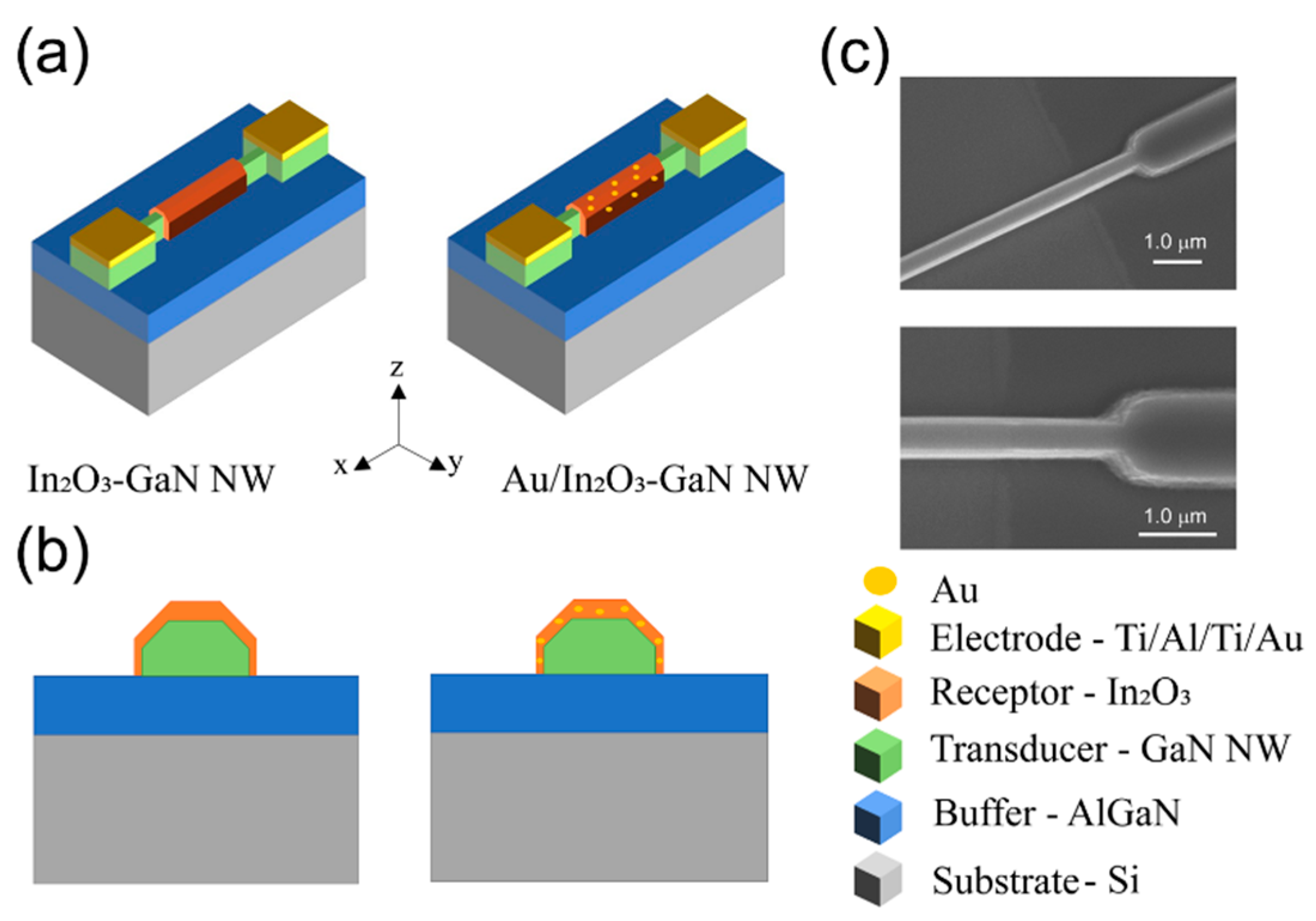
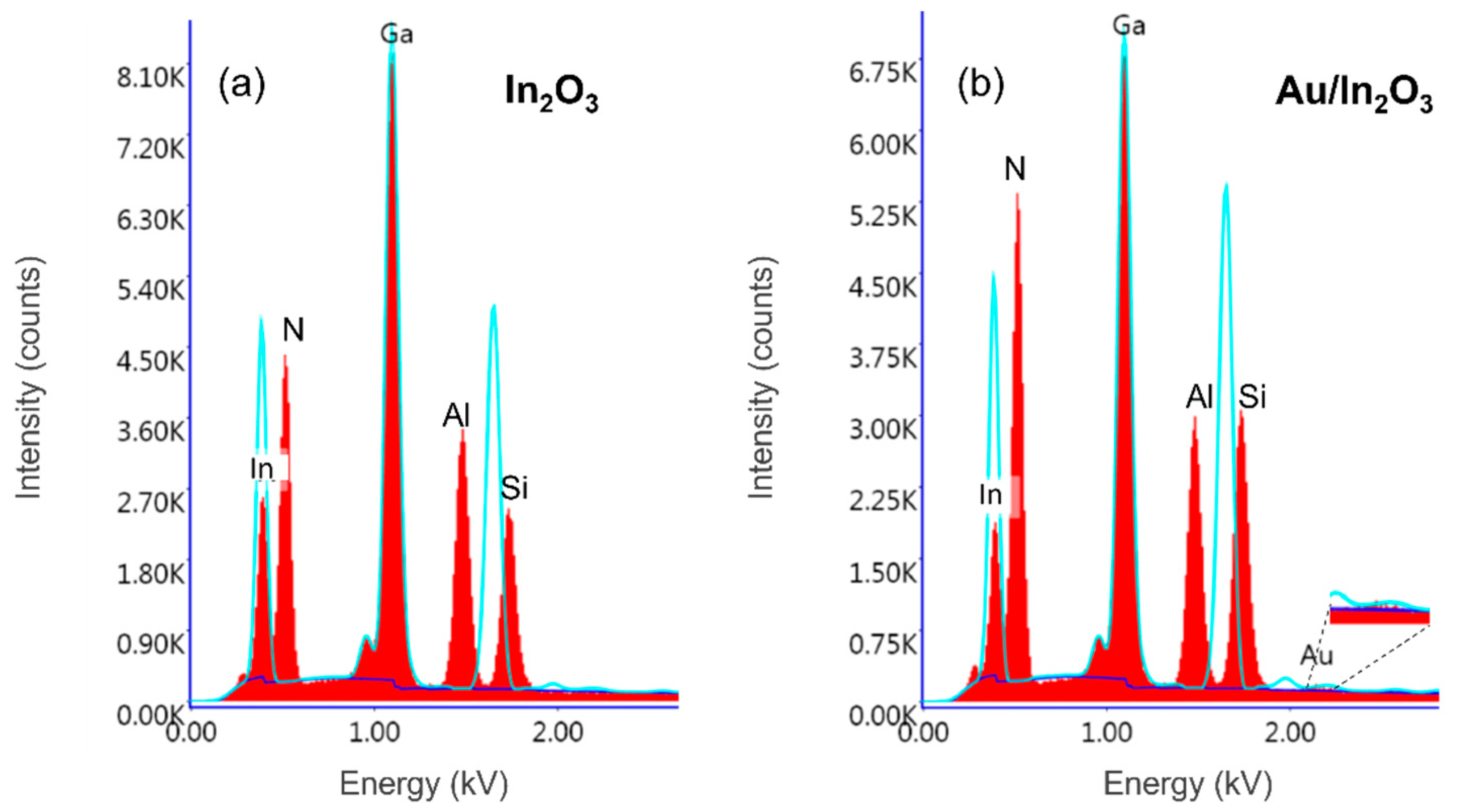
2.1. Device Fabrication & Characterization

The sensors were fabricated following steps similar to those by Khan et al. [24]. An AlGaN buffer layer was first deposited on the Si substrate to minimize lattice mismatch and improve adhesion between Si and GaN NW. Then, the GaN NWs were patterned by stepper-lithography-assisted dry etching, followed by induced coupled plasma etching, using a metal hard mask to protect the GaN NW. The nanowire width target ranges between 200 and 400 nm. Subsequently, electrodes composed of a Ti/Al/Ti/Au metal stack were deposited on top of the GaN layer to form ohmic contacts. Following this, RF magnetron sputtering was used to deposit a thin layer of In2O3 (in the range of 5–10 nm) on top of the exposed GaN NW, which, for a subset of sensors, was followed by the deposition of 1 nm evaporated Au nanolayer on top of the In2O3 layer. For brevity, these two groups of sensors will be referred to as In2O3 and Au/In2O3, respectively, in the figure below. Finally, rapid thermal annealing (RTA) at 700 °C was performed to crystalize the receptor layers and improve ohmic contacts. The devices were characterized by Zeiss Auriga-Field Emission Scanning Electron Microscope (SEM) with energy dispersive spectroscopy (SEM w/EDS). Figure 1 shows schematics and SEM micrographs of the finished based sensors. Several sensors from each group were wire-bonded and mounted onto an array board chamber for testing.
EDS analysis was performed to characterize the composition of In2O3 and Au/In2O3 sensors, as observed in Figure 2a,b.
Figure 2a,b both reveal the presence of In, N, O, Ga, Al, and Si with peaks located at 0.365 kV, 0.392 kV, 0.525 kV, 1.098 kV, and 1.486 kV, respectively. The presence of a small peak of Au at 2.1 kV is observed in the inset of Figure 2b. A corresponding quantity of 0.11 measured in weight % confirms the deposition of a small layer of Au on the Au/In2O3 sensors. Details of EDS spectra values quantified in atomic % and weight % for Ga, N, and Au elements are listed in Table 1.

2.2. Gas Sensor Measurement

During testing, the devices were biased at 5V DC. UV LEDs were mounted within the chamber 10 mm above the sensors, providing constant illumination for the duration of testing. Two UV light wavelengths were consecutively used: 265 nm and 365 nm. Both 265 nm and 365 nm were selected as their photon energies (4.6 eV and 3.4 eV, respectively) are both larger than the GaN bandgap (3.4 eV), a factor that is necessary for electron–hole pair generation. For each wavelength, testing was performed at three power levels: 5 mW, 30 mW, and 60 mW. Optical power was measured using a Network-Power Meter-Model 1928-C. Photoconductivity measurements, humidity testing, and NO2 gas testing (1 ppm and 10 ppm concentration) under various humidity conditions were also conducted. Resistance responses were collected using an Arduino Mega 2560 controlled by NI-LabView software. A gaseous mixture of analyte and carrier gas (breathing air), controlled by mass flow controllers (MFC), was first introduced into a Bronkhorst CEM Evaporator W-101A humidifier prior to flowing into the chamber containing the sensors. The gas mixture was maintained at a constant flow rate of 0.6 slpm and a constant pressure of 5 psi. Figure 3 illustrates the experiment setup for sensor testing.

3. Results and Discussions

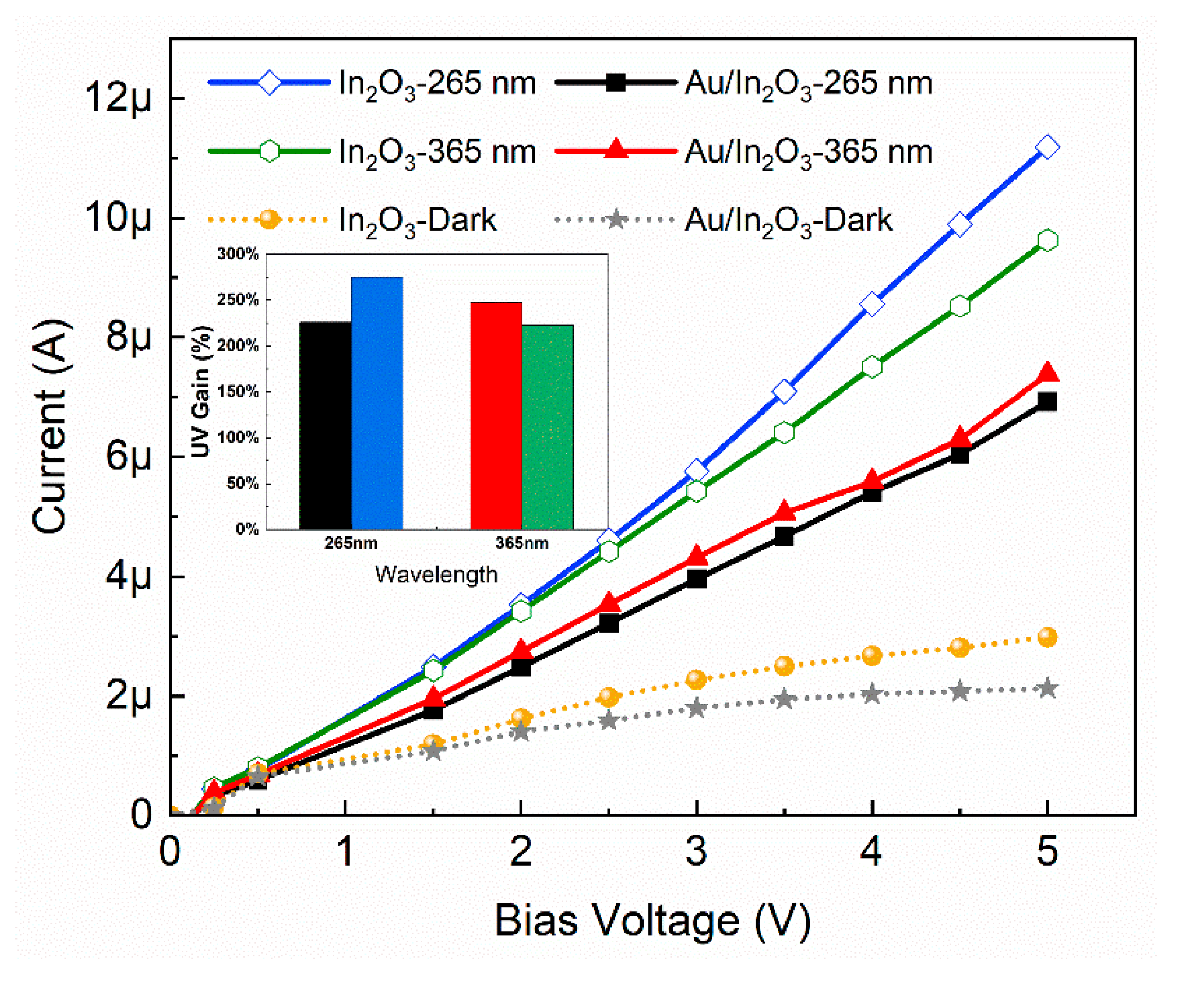
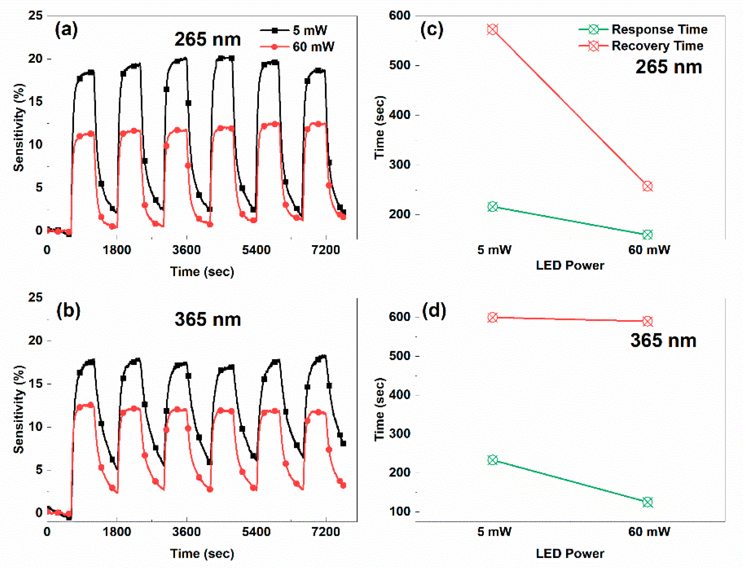
3.1. Photoconductivity

Photoconductivity and humidity testing of the sensors were performed under two illumination conditions: 265 nm at 5 mW (3.3 µW/cm2 irradiance) and 365 nm at 60 mW (1462 µW/cm2 irradiance). Figure 4 shows the I–V characteristics of both In2O3 and Au/In2O3 sensors in the dark and under illumination.
In the dark condition, current levels are rather low for both sensor groups, similar to those observed by Shi et al. [23]. Electron–hole pairs are generated under UV illumination. The In2O3 layer absorbs a small part of the UV light to generate photocarriers, as it is quite thin. Consequently, the density of electrons in the GaN conducting channel increases, thereby explaining the improvement of conductivity between the dark and illuminated conditions observed in Figure 4. Chemisorption of environmental O2 at the sensors surface can also explain the difference in conductivity seen in Figure 4, as described by the following equation [10]:
O 2 + e = O 2 ( a d s )
Oxygen anions will deplete the electrons from the conduction channel of GaN. The amount of generated oxygen anions is small, while the amount of photogenerated electrons in the conducting channel of GaN is large and dominates the conductivity. It should be noted that there are limited active sites for O2 adsorption. Functionalizing In2O3 with Au provides additional active sites for gas adsorption [25]. More O2 molecules can be adsorbed at the Au interface, thus further depleting electrons from the channel. Consequently, the conductivity of Au/In2O3 sensors is lower than that of bare In2O3, as observed in Figure 4. The highest current levels were observed in bare In2O3 sensors, 11.2 µA and 9.6 µA for 265 nm and 365 nm, respectively, while the current of Au/In2O3 sensors diminished (6.9 µA and 7.2 µA). The inset in Figure 4 shows the UV response gain, defined as:
U V G a i n = I U V I d a r k I d a r k
where IUV represents the sensor current under UV illumination and Idark the current under the dark condition. It is interesting to note that the obtained UVGain (250%) under low power illumination at (265 nm, 5 mW) is comparable to that obtained under much higher power illumination at (365 nm, 60 mW). Photoconductivity results indicate that using the 265 nm LED makes it possible for the sensor to be operated at 12 times less power than when using the 365 nm LED, without sacrificing any UVGain. Power reduction is an essential aspect when designing portable devices that rely on batteries.

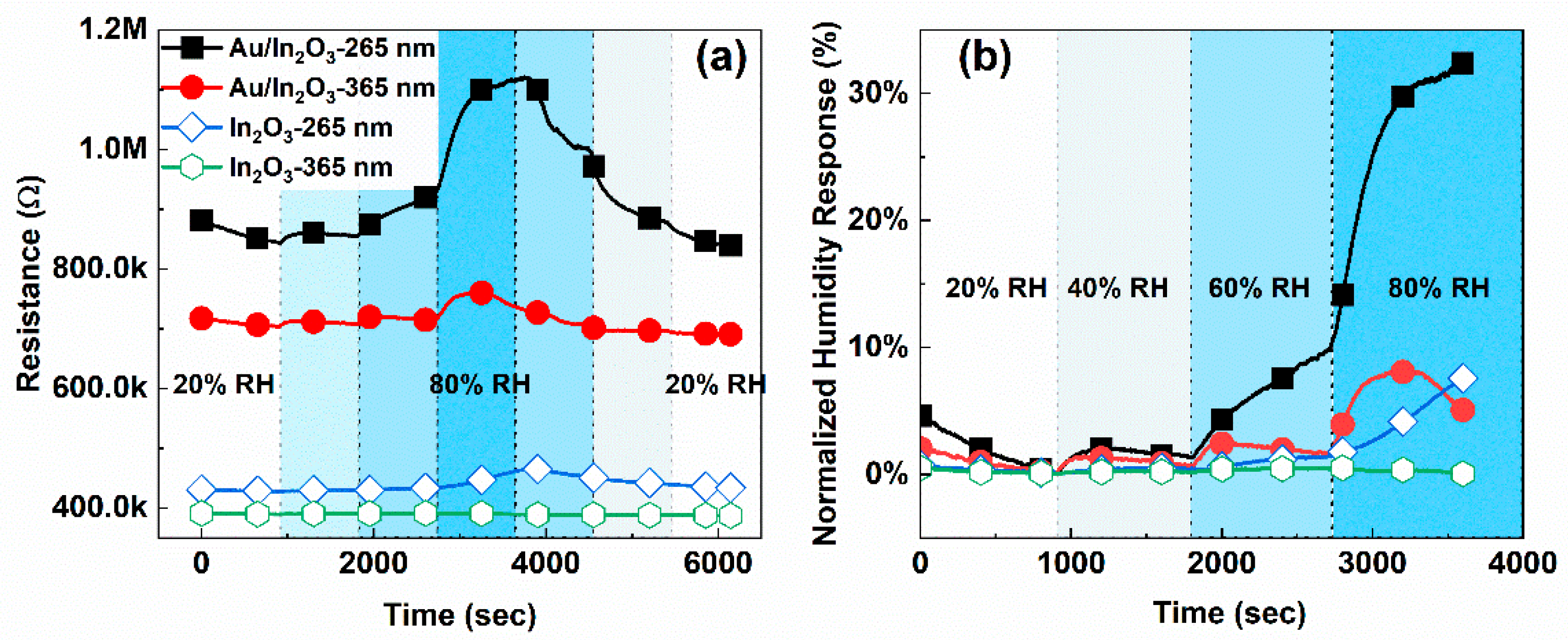
3.2. Humidity Response

The performance of the sensors under the illuminated condition was evaluated for relative humidity (RH) in the range from 20% RH to 80% RH at room temperature (20 °C). The “Humidity Response” HR was defined by the relationship:
H R = R a c t u a l R 20 % R 20 %
where Ractual is the resistance at the measured humidity, and R20% represents the baseline resistance at 20% RH. Each sensor was sequentially tested for 900 s at RH of 20%, 40%, 60%, and 80%. Figure 5a,b show the results of the HR experiments.
At low humidity (<40% RH), all devices displayed a relatively low response to water adsorption under both illumination conditions, with the response deviating less than 5% from the baseline. Mostly, this small change in resistivity is due to chemosorbed water molecules with the metal oxide layer and photogenerated carriers [26]. At medium-to-high humidity (40–80% RH), resistance levels started to increase. Water layers accumulated on top of the chemosorbed layer, promoting proton (H+) hopping [26]. Protons transfer from one molecule to the next by the exchange of a hydrogen bond which generates a change in conductivity. At elevated humidity (80% RH), more water layers accrued, providing additional paths for proton hopping and causing a drastic increase in device resistance. Moreover, water can condensate due to the capillary effect and infiltrate the nanopores, offering further conduction channel paths. This is known as the Grotthuss mechanism [27]. In addition, OH can be generated from H2O under UV irradiation. The OH will form hydroxyl bond OH on the surface and deplete the electrons of n-type GaN, leading to an increase in resistance [28]. Au/In2O3 sensors produced a more pronounced response at elevated humidity compared to bare In2O3 sensors. As seen in Figure 5b, the humidity response of Au/In2O3 sensors sharply increased to 34%, whereas a relatively low response of 7% is observed for In2O3 under 265-nm illumination. Owing to its high catalytic proprieties, Au facilitates the dissociation of water molecules, and these separated species contribute to the increase in resistance. Interestingly, bare In2O3 devices illuminated under 365 nm did not respond to the change in humidity. An important observation from Figure 5 is that sensors illuminated at 265 nm showed a greater response to humidity increase compared to those illuminated at 365 nm. The LED power level may be playing an important role here on the adsorption/desorption rate, as well as on water molecules dissociation. Since (365 nm, 60 mW) irradiates at higher power, higher numbers of photogenerated carriers are available to react with dissociated water, accelerating its desorption rate and, hence, leading to stable response compared to (265 nm, 5 mW). Robust and stable sensors are more desired for environmental monitoring, as outdoor humidity often fluctuates.

3.3. NO2 Response under Various LED Power and Wavelengths

After photoconductivity and humidity testing, the evaluation of NO2 detection was performed. In the presence of NO2, three possible surface reactions can occur, leading to a change in resistivity, measured by the sensitivity S:
S = R N O 2 R a i r R a i r
where R N O 2 is the sensor’s resistance in the presence of NO2, and Rair represents the baseline resistance under ambient air environment. In the first reaction, NO2 interacts with the pre-adsorbed oxygen ion forming a NO2 ion and an oxygen gas molecule. Secondly, two molecules of NO2 interact with the pre-adsorbed oxygen ion and photogenerated electron at the surface, producing two NO3 ions. Finally, in the third reaction, NO2 directly reacts with a photogenerated electron at the surface, producing NO2 [6,7,8,9,10]. Figure 6a,b show the transient response of the Au/In2O3 sensors for 1 ppm NO2 detection at the fixed humidity level of 40% and under three LED power levels (5 mW, 30 mW, 60 mW).
An increase in resistance upon exposure to NO2 is observed, confirming the oxidation type of NO2 gas. NO2 and the pre-adsorbed oxygen attract electrons at the surface, leading to an increase in the depletion layer width, causing a large increase in the sensor resistance. Figure 6c,d show NO2 sensitivity at different LED power levels, along with the respective irradiances measured at the sensor surface. For the same power level, sensitivity is lower at a higher wavelength. For example, at 30 mW, the sensitivity was 23% under 265 nm and 15% at 365 nm. The reason behind this remains a complicated question which, despite many previous efforts to answer it, still remains open [6,29]. A notable observation is that the highest sensitivity (29%) was obtained at the lowest power (5 mW) for both wavelengths and that sensitivity degrades with increasing power. For example, sensitivity is reduced from 29% to 20% when the 265 nm LED power is raised from 5 mW (corresponding to an irradiance of 1.1 µW/cm2) to 60 mW (600 µW/cm2). A similar trend is observed for 365 nm illumination. This behavior agrees with Zhao’s work [30].
Although sensitivity increases with the decreasing power of UV LED, Figure 7c,d show that response and recovery times decrease upon exposure to 1 ppm NO2 with increasing power for both wavelengths. For instance, response time under 365 nm illumination decreased from 233.3 s at 5 mW to 159.6 s at 60 mW power. Interestingly, recovery time drastically decreases at higher LED power for 265 nm: from 572.9 s to 257.4 s. However, sensors under 365 nm illumination have a slow recovery time (i.e., more than 600 s). It is not completely understood why this is, but it can perhaps be explained by considering the newly proposed role of light-activated NO2 [9] and absorption depth of light where the electrons/holes are generated in the semiconductor. Our devices Au/In2O3 demonstrate good short-term repeatability over 6 cycles of exposure to 1 ppm NO2, as observed in Figure 7a,b. However, a slight degradation in sensor sensitivity is observable after 2 months, as evidenced by Figure S1a. This could be caused by the oxidation of our sensors. Finally, our Au/In2O3 sensors have excellent selectivity toward NO2 compared to other gases, such as SO2, H2S, or HCN. Note that the Au/In2O3 did not respond to CO nor NH3, as seen in Figure S1b. Our results indicate that LED power can be optimized for different applications needs.

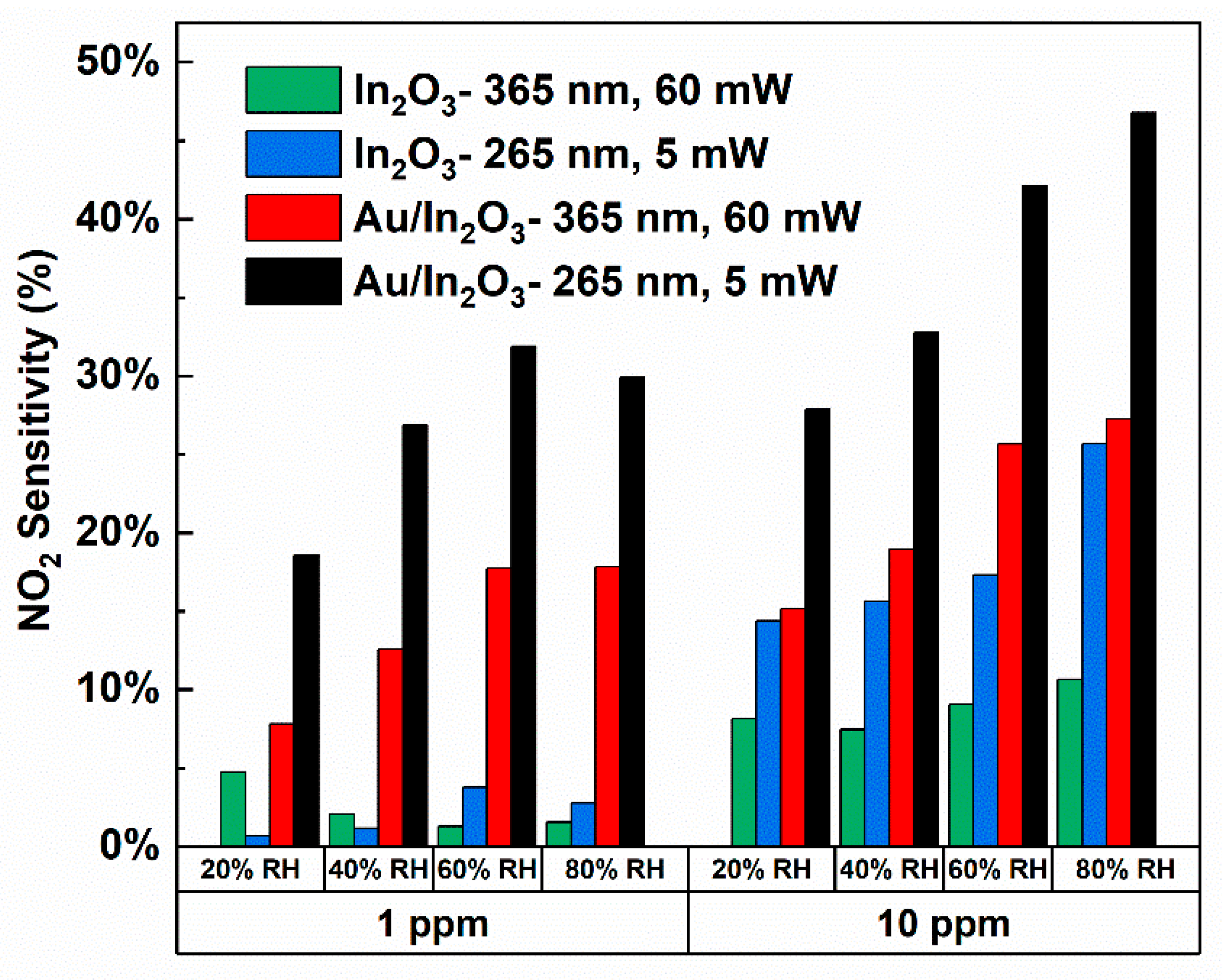
3.4. NO2 Response at Various Relative Humidity Levels

Figure 8 shows the sensitivity to 1 ppm and 10 ppm NO2 detection at various relative humidity levels. In this experiment, two LED conditions were used: (265 nm, 5 mW) and (365 nm, 60 mW).
It was consistently observed that the Au/In2O3 sensors outperformed the bare In2O3 sensors. At 1 ppm, bare In2O3 sensors suffered from a low response rate (<5%). The gas sensing enhancement of Au/In2O3 sensors can be explained by the following two mechanisms. Firstly, the depletion layer modification caused by the presence of Au (work function 5.1 eV compared to 4.3 eV for GaN) causes electrons from the In2O3 to migrate toward the Au nanolayer and react with NO2 [31,32,33,34,35,36,37]. Secondly, due to its high catalytic proprieties, Au allows for an easier dissociation of NO2 and water molecules, known as spillover effect [38]. The separated species transfer toward the In2O3 layer, thereby altering the sensor resistance due to the concentration increase in the Au-induced active adsorption sites. For instance, at (1 ppm, 40% RH, 265 nm), Au/In2O3 exhibited a sensitivity of 27%, while the In2O3 sensors only showed 2% sensitivity. At (10 ppm, 40% RH, 265 nm), response of the In2O3 sensors was 16%, which increased to 33% for the Au/In2O3 sensors. Maximum sensitivities of 32% and 42% were achieved with the Au/In2O3 sensors under illumination at (265 nm, 5 mW) for 1 ppm and 10 ppm concentration, respectively. Remarkably, the NO2 response signals did not degrade with increasing humidity. At higher concentrations, sensitivity increased linearly with increasing humidity. One possible explanation might be that water molecules introduce an additional electron cloud that is favorable to NO2 adsorption due to its electrophilic nature.
Table 2 provides a comparison between the present work and the state of the art for NO2 sensing. For instance, Redeppa et al. investigated the functionalizing of a GaN thin film layer with deoxyribonucleic acid (DNA-CTMA/GaN). The sensor’s response was enhanced with UV illumination at 254 nm and 364 nm, similar to our work. At 10 ppm, the resulting sensitivity was around 10% for both wavelengths, a percentage which is lower compared to our sensor’s response of 42% [39]. Recently, NO2 sensing has also been demonstrated using a heterostructure of graphitic carbon nitride on GaN nanorods (g-C3N4/GaN NR) illuminated at 392 nm at room temperature. Despite having a faster response/recovery time and lower limit of detection (500 ppb) than our sensors, the g-C3N4/GaN NR sensor’s response at 1 ppm was 10% lower than that of our Au/In2O3 sensor, which had a 27% response rate [40]. Sun et al. reported a response of 1.1% to a 1 ppm concentration of an AlGaN/GaN HMET sensor with a built-in microheater [41]. The microheater produces 200 mW, which is about 40 times more than the minimum LED power required for the present sensors. Shin et al. [42] demonstrated that a GaN NW sensor functionalized with graphene (G/GaN NW) could reach a response of 8% to 10 ppm NO2 under 40% RH using LED with wavelengths ranging from 265–350 nm, whereas, under the same conditions, the present sensors exhibited a response of 37%. Recently, several studies have reported excellent sensitivity to NO2 using In2O3 gas sensors with different morphologies. Ueda [34] reported an Au-loaded porous In2O3 sensitivity of 900% to 1 ppm NO2, which is far greater than our sensor’s response. Chen et al. [43] demonstrated that an In2O3/Zn nanofiber sensor could achieve a 130% sensitivity to 10 ppm. However, those In2O3-based sensors operated at a relatively high temperature (100 °C), which increases power consumption. Our sensors achieved reasonable sensitivity with a low power consumption.

4. Conclusions

In summary, GaN NW-based sensors functionalized with In2O3 and Au/In2O3 sensors were presented for NO2 sensing. Photoconductivity results exhibited lower current levels in Au/In2O3-functionalized GaN NW sensors compared to In2O3-functionalized ones. However, the Au/In2O3 sensors consistently demonstrated a superior sensitivity to NO2 than the In2O3 sensors at all tested humidity conditions. The highest sensitivities of 27% and 42% were achieved using the Au/In2O3 sensors under low-power illumination at (265 nm, 5 mW) for 1 ppm and 10 ppm concentrations, respectively. More importantly, the results show the achievement of significant power reduction (×12) when using (265 nm, 5 mW) UV illumination rather than (365 nm, 60 mW), without sacrificing sensitivity. This combination of power reduction and high NO2 sensitivity makes our Au/In2O3-GaN NW sensors an excellent candidate for portable and smart sensor integration.

Supplementary Materials

The following supporting information can be downloaded at: https://www.mdpi.com/article/10.3390/chemosensors10100405/s1, Figure S1: (a) Long-term stability of Au/In2O3 at 5 mW and 60 mW LED power. (b) Selectivity of In2O3 and Au/In2O3 sensors under (265 nm, 5 mW) illumination.

Author Contributions

Conceptualization, A.M. and Q.L.; methodology, Q.L.; software, H.J.Y.; validation, J.R., P.R. and X.W.; formal analysis, J.R. and X.W.; investigation, J.R.; resources, A.M., H.J.Y. and Q.L.; data curation, J.R., P.R. and X.W.; writing—original draft preparation, J.R.; writing—review and editing, Q.L. and D.E.I.; visualization, J.R.; supervision, Q.L. and A.M.; project administration, Q.L. and A.M.; funding acquisition, A.M. and Q.L. All authors have read and agreed to the published version of the manuscript.

Funding

This research was funded by NASA research grant on hybrid gas sensors and Virginia Microelectronics Consortium (VMEC) research grant.

Institutional Review Board Statement

Not applicable.

Informed Consent Statement

Not applicable.

Data Availability Statement

Not applicable.

Acknowledgments

The authors would like to acknowledge the support of NASA research grant on hybrid gas sensors and Virginia Microelectronics Consortium (VMEC) research grant.

Conflicts of Interest

The authors declare no conflict of interest.

References

  1. Arshak, K.; Moore, E.; Lyons, G.M.; Harris, J.; Clifford, S. A Review of Gas Sensors Employed in Electronic Nose Applications. Sens. Rev. 2004, 24, 181–198. [Google Scholar] [CrossRef] [Green Version]
  2. Fine, G.F.; Cavanagh, L.M.; Afonja, A.; Binions, R. Metal Oxide Semi-Conductor Gas Sensors in Environmental Monitoring. Sensors 2010, 10, 5469–5502. [Google Scholar] [CrossRef] [PubMed] [Green Version]
  3. Penza, M.; Cassano, G.; Rossi, R.; Alvisi, M.; Rizzo, A.; Signore, M.A.; Dikonimos, T.; Serra, E.; Giorgi, R. Enhancement of Sensitivity in Gas Chemiresistors Based on Carbon Nanotube Surface Functionalized with Noble Metal (Au, Pt) Nanoclusters. Appl. Phys. Lett. 2007, 90, 173123. [Google Scholar] [CrossRef]
  4. Singhal, A.V.; Charaya, H.; Lahiri, I. Noble Metal Decorated Graphene-Based Gas Sensors and Their Fabrication: A Review. Crit. Rev. Solid State Mater. Sci. 2017, 42, 499–526. [Google Scholar] [CrossRef]
  5. Lee, J.-H.; Mirzaei, A.; Kim, J.-Y.; Kim, J.-H.; Kim, H.W.; Kim, S.S. Optimization of the Surface Coverage of Metal Nanoparticles on Nanowires Gas Sensors to Achieve the Optimal Sensing Performance. Sens. Actuators B Chem. 2020, 302, 127196. [Google Scholar] [CrossRef]
  6. Espid, E.; Taghipour, F. UV-LED Photo-Activated Chemical Gas Sensors: A Review. Crit. Rev. Solid State Mater. Sci. 2016, 42, 416–432. [Google Scholar] [CrossRef]
  7. Xu, F.; HO, H.-P. Light-Activated Metal Oxide Gas Sensors: A Review. Micromachines 2017, 8, 333. [Google Scholar] [CrossRef] [Green Version]
  8. Kumar, R.; Liu, X.; Zhang, J.; Kumar, M. Room-Temperature Gas Sensors under Photoactivation: From Metal Oxides to 2D Materials. Nano-Micro Lett. 2020, 12, 164. [Google Scholar] [CrossRef]
  9. Geng, X.; Liu, X.; Mawella-Vithanage, L.; Hewa-Rahinduwage, C.C.; Zhang, L.; Brock, S.L.; Tan, T.; Luo, L. Photoexcited NO2 Enables Accelerated Response and Recovery Kinetics in Light-Activated NO2 Gas Sensing. ACS Sens. 2021, 6, 4389–4397. [Google Scholar] [CrossRef]
  10. Šetka, M.; Claros, M.; Chmela, O.; Vallejos, S. Photoactivated Materials and Sensors for NO2 Monitoring. J. Mater. Chem. C 2021, 9, 16804–16827. [Google Scholar] [CrossRef]
  11. Wang, H.; Zhou, L.; Liu, Y.; Liu, F.; Liang, X.; Liu, F.; Gao, Y.; Yan, X.; Lu, G. UV-Activated Ultrasensitive and Fast Reversible ppb NO2 Sensing Based on ZnO Nanorod Modified by Constructing Interfacial Electric Field with In2O3 Nanoparticles. Sens. Actuators B Chem. 2020, 305, 127498. [Google Scholar] [CrossRef]
  12. Weiher, R.L.; Ley, R.P. Optical Properties of Indium Oxide. J. Appl. Phys. 1966, 37, 299–302. [Google Scholar] [CrossRef]
  13. Zhang, H.; Xu, X.; Zhu, Y.; Bao, K.; Lu, Z.; Sun, P.; Sun, Y.; Lu, G. Synthesis and NO2 Gas-Sensing Properties of Coral-like Indium Oxide via a Facile Solvothermal Method. RSC Adv. 2017, 7, 49273–49278. [Google Scholar] [CrossRef] [Green Version]
  14. Xiao, B.; Zhao, Q.; Wang, D.; Ma, G.; Zhang, M. Facile Synthesis of Nanoparticle Packed In2O3 Nanospheres for Highly Sensitive NO2 Sensing. New J. Chem. 2017, 41, 8530–8535. [Google Scholar] [CrossRef]
  15. Prajapati, C.S.; Sahay, P.P. Influence of in Doping on the Structural, Optical and Acetone Sensing Properties of ZnO Nanoparticulate Thin Films. Mater. Sci. Semicond. Process. 2013, 16, 200–210. [Google Scholar] [CrossRef]
  16. Aluri, G.S.; Motayed, A.; Davydov, A.V.; Oleshko, V.P.; Bertness, K.A.; Rao, M.V. Nitro-Aromatic Explosive Sensing Using GaN Nanowire-Titania Nanocluster Hybrids. IEEE Sens. J. 2013, 13, 1883–1888. [Google Scholar] [CrossRef]
  17. Toda, K.; Furue, R.; Hayami, S. Recent Progress in Applications of Graphene Oxide for Gas Sensing: A Review. Anal. Chim. Acta 2015, 878, 43–53. [Google Scholar] [CrossRef] [PubMed]
  18. Gawali, S.R.; Patil, V.L.; Deonikar, V.G.; Patil, S.S.; Patil, D.R.; Patil, P.S.; Pant, J. Ce Doped NiO Nanoparticles as Selective NO2 Gas Sensor. J. Phys. Chem. Solids 2018, 114, 28–35. [Google Scholar] [CrossRef]
  19. Walker, J.M.; Akbar, S.A.; Morris, P.A. Synergistic Effects in Gas Sensing Semiconducting Oxide Nano-Heterostructures: A Review. Sens. Actuators B Chem. 2019, 286, 624–640. [Google Scholar] [CrossRef]
  20. Reddeppa, M.; Park, B.-G.; Murali, G.; Choi, S.H.; Chinh, N.D.; Kim, D.; Yang, W.; Kim, M.-D. NOx Gas Sensors Based on Layer-Transferred N-MoS2/P-GaN Heterojunction at Room Temperature: Study of UV Light Illuminations and Humidity. Sens. Actuators B Chem. 2020, 308, 127700. [Google Scholar] [CrossRef]
  21. Khan, M.A.H.; Rao, M.V. Gallium Nitride (GaN) Nanostructures and Their Gas Sensing Properties: A Review. Sensors 2020, 20, 3889. [Google Scholar] [CrossRef] [PubMed]
  22. Aluri, G.S.; Motayed, A.; Davydov, A.V.; Oleshko, V.P.; Bertness, K.A.; Sanford, N.A.; Rao, M.V. Highly Selective GaN-Nanowire/TiO2-Nanocluster Hybrid Sensors for Detection of Benzene and Related Environment Pollutants. Nanotechnology 2011, 22, 295503. [Google Scholar] [CrossRef] [PubMed] [Green Version]
  23. Shi, C.; Rani, A.; Thomson, B.; Debnath, R.; Motayed, A.; Ioannou, D.E.; Li, Q. High-Performance Room-Temperature TiO2-Functionalized GaN Nanowire Gas Sensors. Appl. Phys. Lett. 2019, 115, 121602. [Google Scholar] [CrossRef]
  24. Khan, M.A.H.; Thomson, B.; Yu, J.; Debnath, R.; Motayed, A.; Rao, M.V. Scalable Metal Oxide Functionalized GaN Nanowire for Precise SO2 Detection. Sens. Actuators B Chem. 2020, 318, 128223. [Google Scholar] [CrossRef]
  25. Liu, C.; Kuang, Q.; Xie, Z.; Zheng, L. The Effect of Noble Metal (Au, Pd and Pt) Nanoparticles on the Gas Sensing Performance of SnO2-Based Sensors: A Case Study on the {221} High-Index Faceted SnO2 Octahedra. CrystEngComm 2015, 17, 6308–6313. [Google Scholar] [CrossRef]
  26. Addabbo, T.; Cappelli, I.; Fort, A.; Mugnaini, M.; Panzardi, E.; Vignoli, V.; Viti, C. The Effect of Au Nanoparticle Addition on Humidity Sensing with Ultra-Small TiO2 Nanoparticles. Chemosensors 2021, 9, 170. [Google Scholar] [CrossRef]
  27. Miyake, T.; Rolandi, M. Grotthuss Mechanisms: From Proton Transport in Proton Wires to Bioprotonic Devices. J. Phys. Condens. Matter 2015, 28, 023001. [Google Scholar] [CrossRef]
  28. Munuera, G.; Rives-Arnau, V.; Saucedo, A. Photo-Adsorption and Photo-Desorption of Oxygen on Highly Hydroxylated TiO2 Surfaces. Part 1.—Role of Hydroxyl Groups in Photo-Adsorption. J. Chem. Soc. Faraday Trans. 1 Phys. Chem. Condens. Phases 1979, 75, 736. [Google Scholar] [CrossRef]
  29. Giberti, A.; Fabbri, B.; Gaiardo, A.; Guidi, V.; Malagù, C. Resonant Photoactivation of Cadmium Sulfide and Its Effect on the Surface Chemical Activity. Appl. Phys. Lett. 2014, 104, 222102. [Google Scholar] [CrossRef]
  30. Zhao, D.; Huang, H.; Chen, S.; Li, Z.; Li, S.; Wang, M.; Zhu, H.; Chen, X. In Situ Growth of Leakage-Free Direct-Bridging GaN Nanowires: Application to Gas Sensors for Long-Term Stability, Low Power Consumption, and Sub-ppb Detection Limit. Nano Lett. 2019, 19, 3448–3456. [Google Scholar] [CrossRef]
  31. Hwang, J.; Jung, H.; Shin, H.-S.; Kim, D.-S.; Kim, D.S.; Ju, B.-K.; Chun, M. The Effect of Noble Metals on CO Gas Sensing Properties of In2O3 Nanoparticles. Appl. Sci. 2021, 11, 4903. [Google Scholar] [CrossRef]
  32. Gogurla, N.; Sinha, A.K.; Santra, S.; Manna, S.; Ray, S.K. Multifunctional Au-ZnO Plasmonic Nanostructures for Enhanced UV Photodetector and Room Temperature NO Sensing Devices. Sci. Rep. 2014, 4, 6483. [Google Scholar] [CrossRef] [Green Version]
  33. Ueda, T.; Boehme, I.; Hyodo, T.; Shimizu, Y.; Weimar, U.; Barsan, N. Enhanced NO2-Sensing Properties of Au-Loaded Porous In2O3 Gas Sensors at Low Operating Temperatures. Chemosensors 2020, 8, 72. [Google Scholar] [CrossRef]
  34. Choi, S.-W.; Jung, S.-H.; Kim, S.S. Significant Enhancement of the NO2 Sensing Capability in Networked SnO2 Nanowires by Au Nanoparticles Synthesized via γ-Ray Radiolysis. J. Hazard. Mater. 2011, 193, 243–248. [Google Scholar] [CrossRef]
  35. Mun, Y.; Park, S.; An, S.; Lee, C.; Kim, H.W. NO2 Gas Sensing Properties of Au-Functionalized Porous ZnO Nanosheets Enhanced by UV Irradiation. Ceram. Int. 2013, 39, 8615–8622. [Google Scholar] [CrossRef]
  36. Shim, Y.-S.; Moon, H.G.; Kim, D.H.; Zhang, L.; Yoon, S.-J.; Yoon, Y.S.; Kang, C.-Y.; Jang, H.W. Au-Decorated WO3 Cross-Linked Nanodomes for Ultrahigh Sensitive and Selective Sensing of NO2 and C2H5OH. RSC Adv. 2013, 3, 10452–10459. [Google Scholar] [CrossRef]
  37. Chen, C.; Zhang, Q.; Xie, G.; Yao, M.; Pan, H.; Du, H.; Tai, H.; Du, X.; Su, Y. Enhancing Visible Light-Activated NO2 Sensing Properties of Au NPs Decorated ZnO Nanorods by Localized Surface Plasmon Resonance and Oxygen Vacancies. Mater. Res. Express 2020, 7, 015924. [Google Scholar] [CrossRef]
  38. Phani, A.R. X-ray Photoelectron Spectrscopy Studies on Pd-Doped SnO2 Liquid Petroleum Gas Sensor. Appl. Phys. Lett. 1998, 71, 2358, Erratum in Appl. Phys. Lett. 1998, 72, 3383–3383. [Google Scholar] [CrossRef]
  39. Reddeppa, M.; Mitta, S.B.; Park, B.-G.; Kim, S.-G.; Park, S.H.; Kim, M.-D. DNA-CTMA Functionalized GaN Surfaces for NO2 Gas Sensor at Room Temperature under UV Illumination. Org. Electron. 2019, 65, 334–340. [Google Scholar] [CrossRef]
  40. Reddeppa, M.; KimPhung, N.T.; Murali, G.; Pasupuleti, K.S.; Park, B.-G.; In, I.; Kim, M.-D. Interaction Activated Interfacial Charge Transfer in 2D G-C3N4/Gan Nanorods Heterostructure for Self-Powered UV Photodetector and Room Temperature NO2 Gas Sensor at ppb Level. Sens. Actuators B Chem. 2021, 329, 129175. [Google Scholar] [CrossRef]
  41. Sun, J.; Sokolovskij, R.; Iervolino, E.; Liu, Z.; Sarro, P.M.; Zhang, G. Suspended AlGaN/GaN HEMT NO2 Gas Sensor Integrated with Micro-Heater. J. Microelectromech. Syst. 2019, 28, 997–1004. [Google Scholar] [CrossRef]
  42. Shin, J.; Han, S.; Noh, S.; Yu, Y.-T.; Kim, J.S. Room-Temperature Operation of Light-Assisted NO2 Gas Sensor Based on GaN Nanowires and Graphene. Nanotechnology 2021, 32, 505201. [Google Scholar] [CrossRef] [PubMed]
  43. Chen, K.; Lu, H.; Li, G.; Zhang, J.; Tian, Y.; Gao, Y.; Guo, Q.; Lu, H.; Gao, J. Surface Functionalization of Porous In2O3 Nanofibers with Zn Nanoparticles for Enhanced Low-Temperature NO2 Sensing Properties. Sens. Actuators B Chem. 2020, 308, 127716. [Google Scholar] [CrossRef]
Figure 1. Schematics of proposed In2O3-GaN-NW-based sensors: (a) device structure, (b) cross-section at the center along y/z-axis, and (c) top view of SEM images of GaN NW.
Chemosensors 10 00405 g001
Figure 2. EDS spectrum of (a) In2O3 and (b) Au/In2O3 sensors. Small peak at 2.1 kV for Au/In2O3 sensors reveals the presence of deposited Au.
Chemosensors 10 00405 g002
Figure 3. Experiment setup for sensor testing.
Chemosensors 10 00405 g003
Figure 4. I–V Characteristics under UV illumination and dark condition; (inset) photoconductivity Gain at 265 nm and 365 nm.
Chemosensors 10 00405 g004
Figure 5. (a) Transient response of the various sensors to humidity change. (b) Normalized response from 20% RH to 80% RH.
Chemosensors 10 00405 g005
Figure 6. Transient response of 1 ppm NO2 for Au/In2O3 sensors at fixed 40% RH under (a) 265 nm and (b) 365 nm irradiance with various LED power. Sensitivity under 265 nm (c) and 365 nm (d) degrades with increasing LED power.
Chemosensors 10 00405 g006
Figure 7. Short-term repeatability response at fixed 20% RH of 1 ppm NO2 for Au/In2O3 sensors under (a) 265 nm and (b) 365 nm with 5 mW and 60 mW LED power. Response time and recovery time improve as LED power increases under 265 nm (c) and 365 nm (d).
Chemosensors 10 00405 g007
Figure 8. Sensitivities to 1 ppm and 10 ppm at various relative humidity.
Chemosensors 10 00405 g008
Table 1. EDS weight and atomic ratio analysis for In2O3 and Au/In2O3 sensors.
In2O3Au/In2O3
ElementWeight %Atomic %Error %Weight %Atomic %Error %
N31.8469.938.2733.7371.738.28
Ga68.1630.072.4766.1528.262.52
Au003.40.110.023.52
Table 2. Comparison of the NO2 sensitivity of the sensors presented in this study with those reported in the literature.
Sensing MaterialConcentrations (ppm)λ (nm)Operating Temp. (°C)Power Consump. (mW)Sensitivity (%)Reference
DNA-CTMA/GaN10264, 364RT-10[39]
g-C3N4/GaN NR1392RT-10[40]
AlGaN/GaN HMET1-3002001.1[41]
G/GaN10265–350RT-8[42]
In2O3/Zn nanofibers1, 10-50-2.38, 130[43]
Au-loaded Porous In2O31-100-900[34]
Au/In2O3 GaN NW1, 10265RT527, 42Present Study
Publisher’s Note: MDPI stays neutral with regard to jurisdictional claims in published maps and institutional affiliations.

