Review

Plasmonic Nanosensors and Metasensors Based on New Physical Mechanisms

1
Key Laboratory of Specialty Fiber Optics and Optical Access Networks, Shanghai University, Shanghai 200444, China
2
State Key Laboratory of Millimeter Waves, School of Information Science and Engineering, Southeast University, Nanjing 210096, China
*
Author to whom correspondence should be addressed.
Chemosensors 2022, 10(10), 397; https://doi.org/10.3390/chemosensors10100397
Submission received: 16 August 2022 / Revised: 24 September 2022 / Accepted: 27 September 2022 / Published: 29 September 2022
(This article belongs to the Special Issue Advanced Bio-Chemical Sensors Based on Plasmonic Nanostructures)

Abstract

:
Plasmonics can bind light to their surface while increasing its intensity. The confinement and enhancement of light allows high–density, independent, subwavelength sensor elements to be constructed in micrometer–sized arrays. Plasmonic nanostructures have been widely used in the sensing field because of their fast, real–time and label–free characteristics. Numerous plasmonic metasensors have been configured for next–generation technologies since the emergence of metamaterials and metasurfaces. Among these applications, the development of high–sensitivity sensors based on new physical mechanisms has received tremendous interest recently. This review focuses on high–sensitivity plasmonic nanosensors and metasensors based on new physical mechanisms, especially based on Fano resonance and the exceptional point (EP). The asymmetric Fano resonance generated by the interference of different resonance modes has a narrower bandwidth, while an EP occurs whenever two resonant modes coalesce both in their resonant frequency and their rate of decay or growth. Both physical mechanisms could tremendously improve the sensitivity of the plasmonic sensors. We summarize the working principles, the latest development status and the development trends of these plasmonic nanosensors and metasensors. It is believed that these new sensing mechanisms can inspire more fruitful scientific research.

1. Introduction

Surface plasmon resonance (SPR) is the resonant coupling of electromagnetic (EM) waves with collective oscillations of free electrons in metals, which is widely used due to the possibility of controlling the properties of light at the nanoscale [1,2]. SPR exists in two forms: one is a transmission mode that exists at the interface between metal and air, called conductive surface plasmon polaritons (SPPs), and the other is a resonant mode that is localized on the surfaces of metal nanoparticles; it is called localized surface plasmon polaritons (LSPs). Due to the characteristics of small spatial scale and local enhancement of field intensity, LSPs have important applications in fields such as surface–enhanced Raman scattering [3,4] and chemical biosensors [5,6]. In particular, the EM field is strongly bound to the vicinity of the nanoparticle, and the LSPs are very sensitive to the particle geometry and permittivity of the surrounding environment. Therefore, LSPs can be designed as sensors with high sensitivity, miniaturization and high integration [7,8,9]. The development of sensors based on SPRs is relatively mature, but it is still a challenge to generate SPRs efficiently, as it requires a prism to implement phase matching, which is one of the reasons that SPRs device are difficult to be highly integrated [10,11]. To realize miniaturized devices, the SPRs excited by a one–dimensional (1D) or two–dimensional (2D) grating coupler [12,13], or the permittivity–near–zero (ENZ) plate [14,15], have been proposed. Another challenge is to detect minute changes in materials under test, such as small molecules with low concentrations near the metal/medium interface. A metamaterial is a composite structure composed of subwavelength elements, and metamaterial sensors are sensitive to changes in the surrounding environment [16,17]. In particular, planar metamaterials have been widely used in the field of ultra–high–sensitivity biosensors because they have strong local and enhanced fields [18,19,20]. The key points of achieving high–sensitivity biosensors based on metamaterials are the ultra–high–quality (Q) factor and small linewidths. However, they still suffer from high radiation loss. Fano resonance is thus introduced to reduce the radiation loss of the structures.
In 1961, Ugo Fano discovered a new type of resonance with an asymmetric spectral line shape when studying the self–ionized states of atoms, and proposed the Fano formula to describe its spectral line shape [21]. In recent years, Fano resonance has been realized in many systems, such as photonic crystal plasmonic nanostructures [21,22,23,24,25], metamaterials [26,27,28,29], etc. In plasmonic structures, Fano resonance results from the coupling of the narrowband sub–radiation mode and broadband super–radiation mode [30,31,32,33]. When the two resonant modes overlap in frequency, the extinction interference occurs, which results in the system scattering being strongly suppressed in a narrow band, thus presenting an asymmetric Fano spectrum line shape in the scattering cross–spectrum. A Fano resonant EM structure can greatly reduce or even completely suppress the radiation loss of the system by using the interference between the hyper–radiation and sub–radiation modes, resulting in a steep dispersion resonance mode [22,31,34,35], high local EM field enhancement [36,37] and high RI sensing [38,39,40]. Fano resonance is widely used in high–sensitivity sensing because of its steep scattering cross–section.
The concept of the exceptional point (EP) was first proposed in the perturbation study of the linear non–Hermitic system [41], which was a unique degeneracy point of the non–Hermitic system. At the EP, the real and imaginary parts of multiple eigenvalues of the system are equal at the same time, respectively. The eigenstates no longer constitute a complete basis vector [42], but, far from the EP, the eigenstates have a complete orthogonal state [43]. The realization of the EP system requires the definition of the equivalent Hamiltonian operator and the degeneracy of the eigenvalues and eigenstates of the Hamiltonian operator. The abnormal optical phenomena near the EP include energy level repulsion, crossover and phase mutation. It has important applications in unidirectional transmission/reflection [44,45,46,47] and improving sensor sensitivity [44,47,48,49,50]. The sensitivity improvement is due to the strong response of the intrinsic frequency to the external disturbance. For the EP sensing system with N eigenvalues, the intensity of the intrinsic splitting (detection signal) is proportional to ε 1 N (ε is the external disturbance), and the change rate of the splitting intensity tends to infinity as ε→0 [51]. The high–order EP system has more complex physical characteristics. For example, by tuning the coupling coefficients between multiple micro–resonators, the relationship between the response order and the EP order of the N–order system is theoretically deduced. Based on this, the fourth–order non–Hermitic sensor is designed, and the sensitivity is increased by more than 100 times compared with the traditional single–ring resonator [51]. However, a high–order EP does not guarantee a high–order response to the applied disturbance, so the general principles for designing high–order EP sensing are of great research significance. The realization of EP sensors in plasmonic structures is an important direction for enhancing the sensitivity, which will guide the discovery of related sensors in the future. The development of new sensors not only reduces the costs of sensors, but also greatly improves their performance, which greatly improves the detection limits of sensors.
In this review, we introduce two types of novel plasmonic nanostructures, which greatly improve the sensitivity of the sensors. The new sensing methods based on Fano resonance and EP, and the specific generation methods and structures that can generate the two resonances, have been summarized. In addition, the development status and future research directions of sensors based on Fano resonance and EP are introduced.

2. Parameters of Plasmonic Sensors

2.1. Quality Factor

The Q factor is defined as the ratio of the energy stored in the system to the energy supplied by the outside for each period at the resonant frequency of the system, when the signal amplitude does not change with time. The resonant frequency of the resonator can be expressed relative to the bandwidth. A high Q factor means that the rate of energy loss of the resonator is slow, the vibration can last for a long time, and the bandwidth is narrow. In practice, the Q factor of the resonator is the ratio of the wavelength divided by the resonant width [52],
Q = λ Δ λ = f Δ f
Here, the Q factor is an important parameter in the design of plasmonic sensors, and a sensor with a high Q factor is more conducive to the detection of resonance offset in the experiment.

2.2. Sensitivity and Figure of Merit

Sensitivity represents the signal conversion capability of the sensor. The definition of sensitivity is not invariant, but is related to the parameters to be tested [52]. For example, the sensor interacts with the analyte touching its surface, and the mass/(sensor surface units) ratio can be assumed as an input variable. If the sensor is sensitive to the analyte bound to the surface, the input signal is the analyte concentration. When the RI of the substance to be measured around the plasmonic structure is changed to a certain amount, the position of the plasmonic resonance in wavelength units is shifted. The corresponding sensitivity can be expressed in units of wavelength ( S λ ) [53]:
S λ = d λ d n
The sensitivity can reflect the performance of the plasmonic sensor to a certain extent, but for the sensor with a large linewidth, which has a low Q factor, the change in the resonance position in the wavelength unit cannot reflect the advantages and disadvantages of the sensor. Defining the resonance displacement with respect to the linewidth is a more meaningful approach. The figure of merit (FOM) is a dimensionless value, which is originally defined as the variation in the resonance displacement with respect to the linewidth. FOM is defined as
FOM = S Γ
where Γ represents the plasmonic linewidth (full width at half maximum), namely the semi–resonant linewidth.
When the RI around the sensor changes very little, the strength of resonance will change with the change in RI. When the position of the resonance does not change, the magnitude of the relative resonance can be expressed as d I I . Thus, we define another dimensionless FOM*:
FOM * = ( ( d I / d n ) I ) m a x = ( S λ ( d I / d n ) I ) m a x

2.3. Limit of Detection

The limit of detection (LOD) is defined as the minimum concentration or mass of a biochemical substance that a sensor can detect on a background signal. In most chemical and biosensors, the detection limit is a key parameter to evaluate the sensing capability and practical value of the device. It determines the lower limit of the range of measurements detected by the sensor. The LOD depends on the resolution of the sensor. The LOD can be expressed as
LOD = 3 σ n S
where σ n and S are the standard deviation of the total noise of the system and the sensitivity, respectively [52]. It can be approximated by summing all the noise variances contributing to the system resolution. In optical sensors, since the LOD is associated with the smallest detectable change, the LOD can be written as
LOD = Δ λ r e s S   or   LOD = Δ I S
Here, Δ λ r e s and Δ I denote the resolution of the measured spectrum. Δ λ r e s is the smallest resolvable change in resonance wavelength. Theoretically, it is independent of the resonance shape or bandwidth, and only depends on the resolution of the measuring instrument. However, there is noise interference in the experimental measurement, so it is difficult to accurately measure the wavelength shift for a resonance with a large line shape. In order to improve the measurement accuracy, the resonant line is often required to have a high Q factor.

3. Fano Resonance–Based Sensors

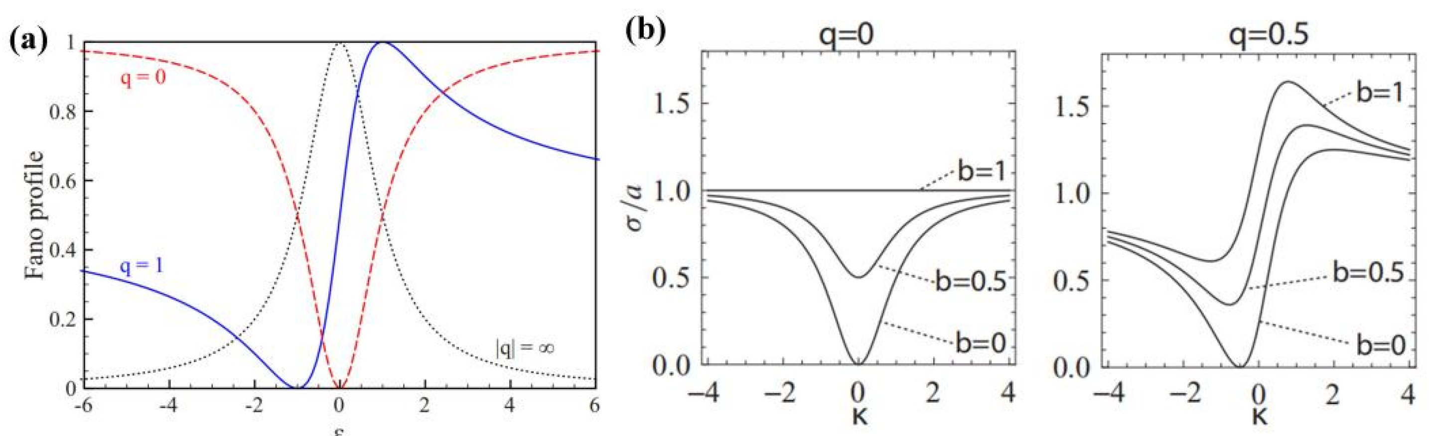
3.1. The Theory of Fano Resonance

The Fano formula proposed by Ugo Fano can be used as a mathematical tool to accurately fit any type of asymmetric spectral line shape. According to the Fano formula, the line shape equation of the scattering cross–section is expressed as [21]
σ ( ω ) = ( q + ε ) 2 1 + ε 2
The Fano parameter is described by q, which presents the asymmetry degree of the spectral line shape. In the equation ε = 2 ( ω ω 0 ) / γ , ω 0 represents the center frequency of Fano resonance, and γ represents the spectral linewidth of Fano resonance. According to the formula of Fano, the scattering cross–section is the smallest when ε = q , and σ m i n = 0 . The scattering cross–section is maximized when ε = 1 q , and σ m a x = 1 + q 2 . When q = 0 , the scattering spectrum shows an inverted Lorenz line shape. When q = 1, a significant asymmetric Fano spectral alignment appears, with its maximum value occurring at the spectral position of ε = 1 q = 1 ( ω = ( 2 ω 0 + γ ) / 2 ) and its minimum value occurring at the spectral position of ε = q = 1 ( ω = ( 2 ω 0 γ ) / 2 ). At this time q , the asymmetric spectral line disappears and the scattering spectrum changes into a symmetric Lorenz line. The scattering cross–section of Fano resonance with different q values is shown in Figure 1a. However, the Fano formula proposed by Ugo Fano does not involve system loss and does not give any physical meaning, so it cannot be well applied to lossy structural systems. An ab initio EM approach to generalize the Fano formula to the case of vectorial fields and lossy materials has been proposed [54,55], and it can be described by the formula
σ a ( ω ) = a ( q + k ) 2 + b 1 + k 2
In this formula, k = ω 2 ω 0 2 2 γ ω 0 is the reduced frequency, and b is called the modulation attenuation factor, which characterizes the intrinsic ohmic heat loss inherent in plasmonic materials. In the case of asymmetric parameter q = 0 , the scattering cross–section exhibits a symmetric Lorenz spectral line shape. When q 0 , the scattering cross–section shows an asymmetric Fano spectral line shape, in which the different signs of the Q factor imply the different non–symmetric orientations of the spectrum. The modulation attenuation factor b characterizes the modulation depth of the Fano resonance, and the larger b is, the larger the ohmic heat loss of the system will be, so the smaller the spectral modulation depth of the Fano resonance will be. Figure 1b demonstrates that the modulation depth of Fano resonance varies with different b values, considering that, in a plasmonic system, the Fano resonance is coupled from a non–radiation mode to a broad radiation mode that is strongly coupled to the incident EM radiation. Firstly, the super–radiation mode has a symmetric Lorenz line, and the scattering cross–section can be expressed as follows:
σ s ( ω ) = a 2 1 + ( q + k ) 2
In the Fano resonance of the plasmonic system, the flat continuous state is replaced by the broadband plasmonic resonance, so the total intensity of the scattering cross–section of the system can be expressed as the product of the symmetric and asymmetric scattering cross–sections:
σ t ( ω ) = σ s ( ω ) σ a ( ω )
The scattering cross–section of a Fano resonance EM structure can be theoretically analyzed by using the above formula.

3.2. Fano Structure and Fano Resonance–Based Sensors

Fano resonance originates from the destructive interference between super–radiation mode and sub–radiation mode. Plasmonic Fano resonance can effectively suppress the radiation loss, which is an effective way to obtain a narrowband spectral response and high local EM field enhancement effects. Compared with conventional LSPs modes, Fano resonance has been proven to have a higher RI sensitivity and Q factor. A Fano resonant EM metastructure has great application prospects in the biological/chemical sensing field. In this section, we will describe the Fano structures and their sensing applications.

3.2.1. Single Metal Nanoparticles

The back scattering and forward scattering cross–sections of a single metallic sphere can be calculated by the Mie solution [56]. The dipole resonance of metal nanostructures is a super–radiation mode, and the spectral linewidth of the formant is wide, which can be directly excited by the incident light. The center frequency of Fano resonance corresponds to the quadrupole resonance of metal nanoparticles, which is a narrowband sub–radiation mode. The coherent coupling between the dipole resonance of the super–radiation mode and the sub–radiation quadrupole resonance leads to the excitation of the non–symmetric Fano resonance in the scattering spectrum [22]. Later, some works studied the conditions of observing the Fano resonance of a single obstacle of finite size under elastic light scattering based on the Mie solution [57]. The Fano resonance of single metal spherical particles usually cannot be clearly shown due to the large intrinsic losses of metal materials. However, limited dissipation can increase the Q factor and enhance the strength of Fano resonance.

3.2.2. Coupled Fano Resonance Structures and Sensors

Symmetric Broken Metal Nanostructures

Broadband super–radiation patterns can be excited in symmetric nanoparticles. If a small asymmetry is introduced into the shape of the nanostructure, the sub–radiation resonance mode can be excited, in which the sub–radiation resonance has small emission damping and cannot be directly excited by the incident EM field; it can only be indirectly excited by the coupling effect with the super–radiation resonance. The Fano resonance is generated by the destructive interference between the narrowband sub–radiation resonance and the wideband super–radiant mode in a single symmetric broken metal nanostructure. Based on this method, a large number of single metal nanostructures with symmetric breaking have been designed to realize Fano resonance, including resonant ring structures [58,59,60], symmetric broken nano–disks [61] and other structures.
Compared with the single symmetry broken metal nanostructures, the arrangement of two or more metal elements can also produce Fano resonance [35,62,63,64]. In this complex structure, the metallic elements all support a wide band of super–radiation resonant modes. However, for the whole structure, the near–field coupling of the metal will excite the narrowband plasmonic mode. By adjusting the arrangement of metal nanoparticles, size and structure, one will be able to tune the Fano resonance. The plasmonic nanostructure consists of two ring/disk cavities (RDCs). The excited dark multipole mode of each RDC induces a sharp multipole Fano resonance. The multipolar modes supported by different RDCs can be tuned independently by changing the sizes. The scattering/absorption of the RDCs is obtained by changing the size of R3 [62]. The wavelength as well as intensity of these resonances can be adjusted effectively by tuning the split angle of the splitting ring (SR), the gap distance between two rings, the width of two rings and the offset of the perfect ring (PR) along the x–axis [64]. The maximum RI sensitivity of the structure exceeds 1225 nm per refractive index unit (RIU), and the figure of merit (FOM) reaches 30.4.

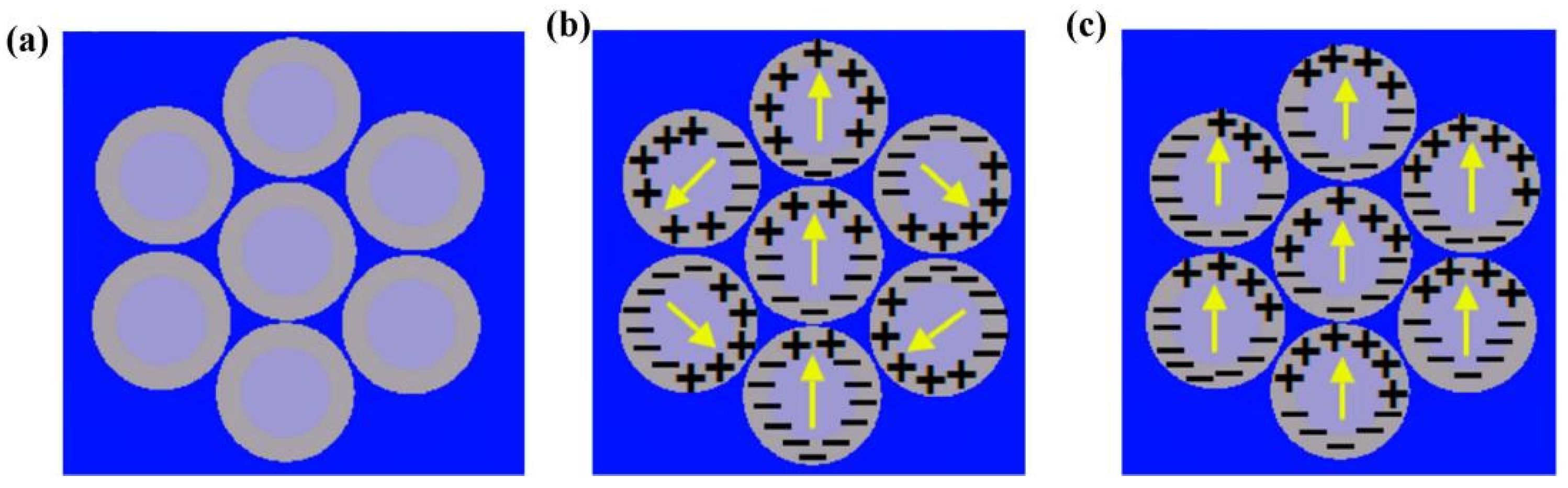
Fano Resonance and Sensors Based on Metal Nanoparticle Polymers

Plasmonic oligomers are one class of the most promising nanoclusters for generating Fano resonances [30,65,66,67]. The plasmonic response of nanoparticle polymers can be regarded as a linear combination of the plasmonic resonance responses of individual nanoparticles. For example, the plasmonic spectral response of a heptamer structure can be regarded as the result of mutual hybridization between the collective plasmon resonance modes of the ring structure composed of the center nanoparticle and six peripheral nanoparticles, as shown in Figure 2a [65]. In the heptamer structure, the dipole moment of the center nanoparticle is almost equal to that of the outer ring structure. When the directions of the charge oscillation are the same, the hybrid bonding mode has a large radiation loss and thus a wide spectral linewidth, as shown in Figure 2b. When the charge oscillation directions are opposite, the total net dipole moment of the hybrid anti–bonding mode is almost zero, as a narrowband sub–radiation resonance, as shown in Figure 2c. A constructive and weak interference between the sub–radiation dark and super–radiation bright modes, as the plasmon resonance modes, causes the appearance of strong Fano resonances in the spectral response of the polymer. In polymer structures, the spectral response of the isoplasmon Fano resonance can be regulated by changing the spacing between metal nanoparticles. When the particle spacing is small, the near–field coupling between nanoparticles is strong, and the spectral response of Fano resonance is more significant.
The excitation of Fano resonance in nanoparticle polymer structures is the result of structural symmetry and does not depend on the shape of individual metal nanoparticles but the aggregation state of nanoparticles. Tight molecular orientations are arranged into plasmonic resonance coupling between nanoclusters, including heterodimers comprising a nanocross and a nanobar [66], the heptamer and octamer clusters of metals [30,66] and anti–symmetric eight–member nanoshell oligomers [67]. A simple heterodimer comprising a nanocross and a nanobar, where plasmonic modes with opposite radiative decay characteristics are excellently overlapped both spectrally and spatially by elaborate tailoring, was designed. Double strong Fano resonances appeared on opposite sides of the spectrum, as expected [66]. Benefiting from the enhanced near–field and reduced spectral linewidth, the gold heptamer exhibits high RI sensitivity, which is 940 nm/RIU, together with a FOM value as large as 20.9, which surpasses that of most other gold oligomers. Aluminum (Al) nanoparticles were arranged into nanoclusters with tight molecular orientations and plasmon resonance coupling between them [65]. Upon quantifying the FOM of the final octamer, the FOM was 7.72. Gold (Au) was deposited on a multilayer substrate composed of β–sic/SiO2/Si layers, and the plasmonic resonance mode was excited on the antisymmetric eight–membered nanoshell oligomers (octamers). Using the geometrical tunability of nanoshells, the excitation and interference of the sub– and super–radiation plasmonic modes were analyzed. It was shown that a multilayer substrate plays a fundamental role in the confinement of optical power in the nanoshell octamer, and results in the formation of a pronounced Fano minimum [67]. The linear FOM was measured based on the plasmon energy differences over the RI variation by immersing the optimized nanostructure in various liquids with different RI, and the remarkable FOM was calculated as 22.25.

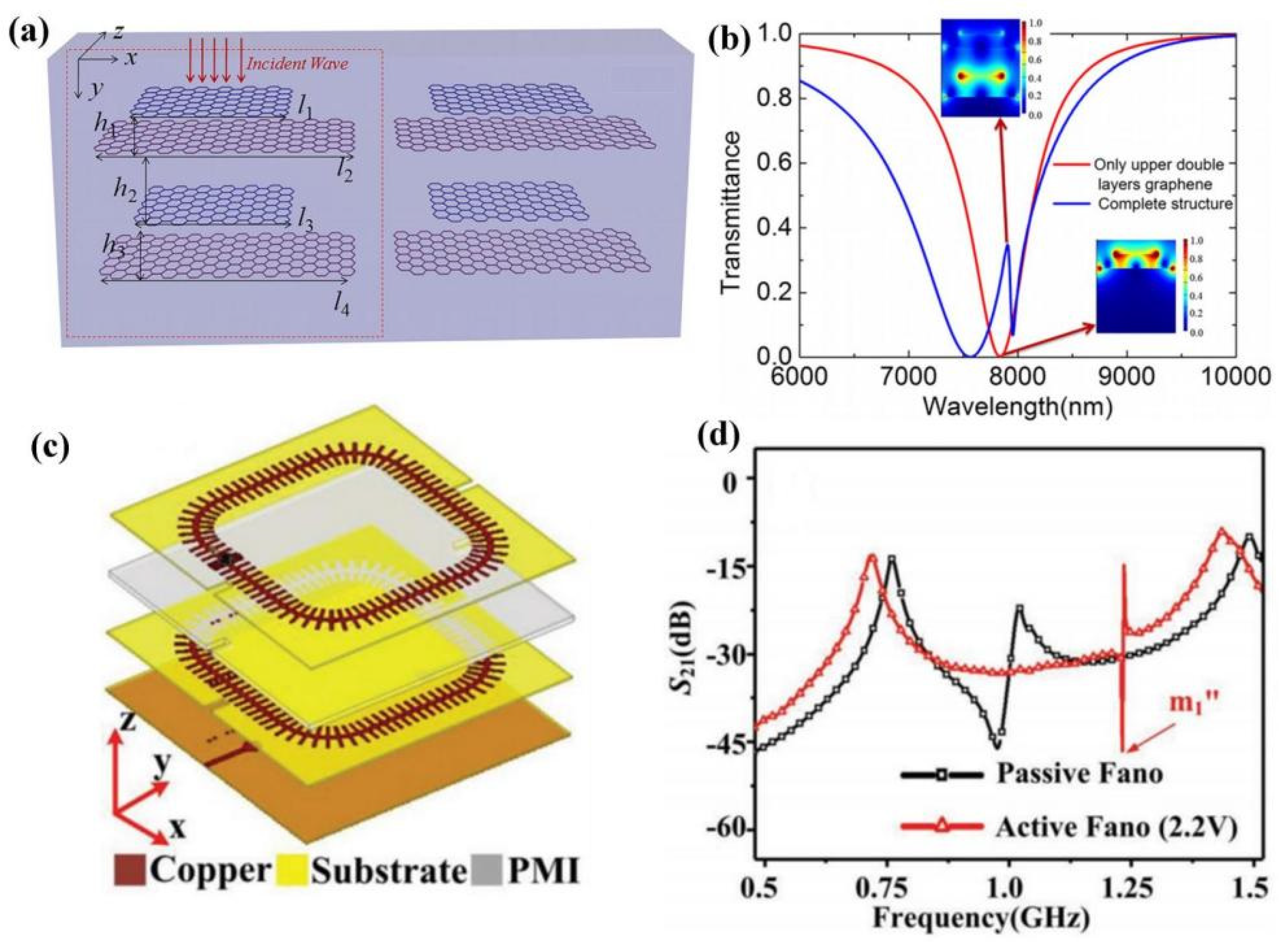
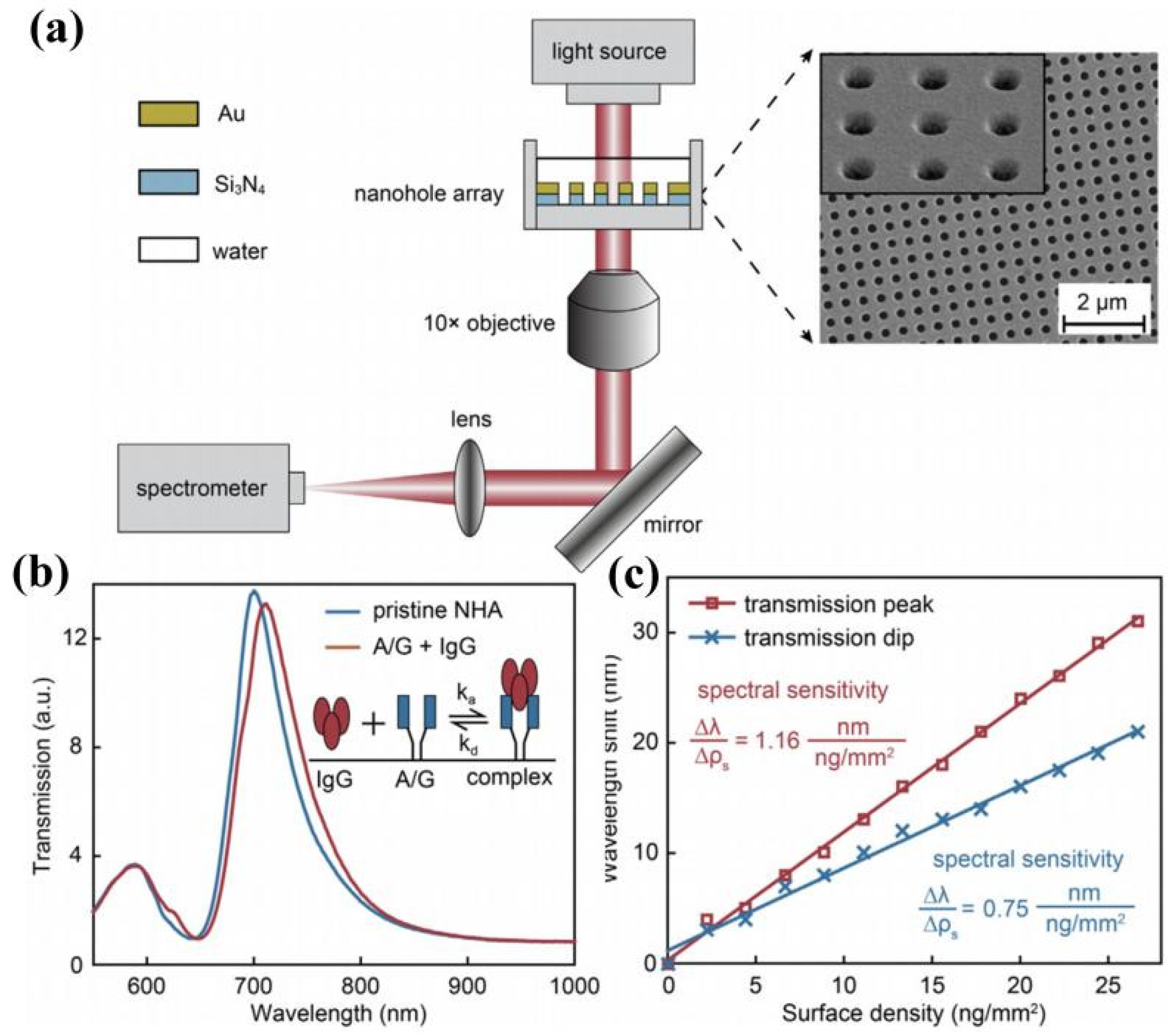
Fano Resonance and Sensors Based on Nanoarray and Metasurfaces

Nanoarray Fano Resonance
In metal nanoarray structures, Fano resonance can be generated by the interference between narrow SPPs in resonant mode and wide LSPs in resonant mode by changing the arrangement and symmetry of the structure. In a recent work, Fano–like resonances were generated in the mid–infrared region by coupling between upper and lower graphene nanoribbons [68]. The resonance could also be effectively controlled by adjusting the geometric parameters of the graphene system, such as the central position of the graphene nanoribbon and the coupling distance between the upper and lower layers of the graphene nanoribbon. In the Al2O3/SiO2 planar waveguide, the plasmonic periodic E–shaped metal nanostructure could excite the quasi–waveguide mode, so as to realize the multichannel Fano transmission. Periodic E–shaped Au nanostructures were placed on top of a Al2O3/SiO2 dielectric slab waveguide, which directly excited the super–radiation bright LSPs mode of the E–shaped nanostructure [69]. The necessary momentum could be provided to couple the diffracted waves of the Au nanostructure array into these quasi–guided modes propagated in the embedded Al2O3 layer, and these quasi–guided modes were non–radiation. Fano–shaped transparency and high reflectance peaks can be obtained by the destructive interference between the broadband plamsonic mode and narrowband quasi–guided modes. It is well known that the linewidths of Fano resonances in nanostructures are large because of huge losses of LSPs (including radiative losses and absorption losses) in metallic nanostructures. This hinders the sensing applications of plasmonic nanoarray structures. At present, some works seek to improve the characteristics of plasmonic Fano resonance by changing the arrangement of the structure. It is found that when the metal nano–groove array is tilted, the linewidth of the Fano resonance in the scattering spectrum is reduced [70]. Figure 3a,b demonstrate that the FOM of the tilted structure is lifted up to 600. The study demonstrated that infrared multi–narrowband tunable plasmonic–induced transparency can be used as a plasmonic sensor. For biochemical sensing, the RI of the detected sample varies minimally in most cases. This E–shaped nanostructure has excellent sensing performance. The results show that the FOM* of the sensor can reach 66,548 in the range of RI 1.3~1.39.
Metasurface Fano resonance
EM metamaterials are artificial composite structures formed by the periodic or non–periodic arrangement of subwavelength units with a certain shape or pattern. Its EM properties are highly dependent on the geometric shape, structure size and array period of the structural units. The artificially engineered nature of EM metamaterials provides an effective strategy to manipulate EM waves. It is easy to realize Fano resonance by changing the physical size of artificial EM materials, and Fano resonance based on metamaterials has been widely studied. Different geometries of artificial metasurface structural elements have been investigated. For example, plasmonic Fano resonances were also investigated in a coupled metasurface consisting of gold nanobars [71]. The destructive interference between different modes supported by bright and dark nanobars leads to the emergence of a sharp asymmetric Fano line shape in the extinction spectrum. Multiple Fano resonances in the near–infrared regime are excited by arranging the L–shaped nanostructure in different ways. Authors also described a multimode structure based on metasurface plasmon Fano resonance operating in the near–infrared band, whose unit structure was a two–binary split nanoring [72]. In most research works, artificial metamaterials with Fano resonance are periodic array structures based on asymmetric resonant ring elements [73,74,75,76,77]. In the asymmetric resonant ring, when one of the gaps is far away from the vertical axis, the difference in resonance frequencies between the two metal wires forming the asymmetric ring is small, leading to a strong coupling between them. By adjusting the asymmetry of the gap, the final anti–phase oscillation in a very narrow frequency range leads to destructive interference and the formation of asymmetric spectral linear Fano resonance. In addition, it is also common to achieve Fano resonance with a unit structure composed of two or more asymmetric resonators. The positions of the two resonant rings can be placed horizontally [78,79,80,81,82], vertically [71,80,83,84,85] or nested [86]. Due to the field enhancement and asymmetric line shape of Fano resonance, and the characteristics of high Q factor and FOM [73,87,88,89], Fano resonance–type EM metastructures have important application value in sensors. Fano resonance is extremely sensitive to the thickness and RI of the measured object, and in order for a solid object of a specific thickness to be measured, the frequency shift of Fano resonance changes linearly with the change in the RI to be measured. However, Fano resonance is also very sensitive to dielectric substrates of different thickness. Therefore, the selection of an appropriate medium thickness has an important impact on the sensitivity of a Fano resonance sensor [73,87]. For example, when an object to be measured at 1.6 um was placed on a metamaterial, it could be seen that the Fano resonance had an obvious frequency shift when the RI changed from n = 1 to n = 1.6, as shown in Figure 4a,b. The calculated sensitivity was as high as 49.3 GHz/RIU (5.7 × 10⁴ nm/RIU) [73]. Some Fano resonant sensors based on artificial metamaterials are summarized in Table 1.
Active Fano resonance
Changing the Fermi level of the graphene layer enables tunable transmission properties in symmetric structures [90,91]. Therefore, the graphene–based structure can achieve active tuning of Fano resonance. When the structure is symmetrically broken at a high Fermi level, we can achieve high Q Fano resonance and quadrupole resonance. The Fermi level of graphene is changed to achieve the electrical tunability of Fano resonance. In addition, the sensitivity of graphene–based metamaterials is higher than that of metal–based plasmonic structures, which facilitates the design of ultra–sensitive sensors. By changing the RI of the object to be measured, the Fano resonant sensor reaches 1.87021 THz/RIU. In graphene layered metamaterials, changing the Fermi level of graphene can achieve destructive interference and Fano resonance in a narrow frequency band, as shown in Figure 5a,b. The layered graphene structure achieves a Fano resonant sensor with an FOM of 9786 and a sensitivity of up to 7885 nm/RIU. The selection and switching of Fano resonance can be realized by adding diodes in artificial metamaterials [92]. Recently, it has been found that placing a low noise amplifier on the resonant structure can effectively overcome the loss of the resonant structure and improve the resonant strength [93,94]. This drawback can be overcome by introducing this idea into Fano–type artificial EM metamaterials [95]. The active Fano structure is shown in Figure 5c. After adding a low noise amplifier, the Q value of Fano resonance can be increased by 58 times, and the resonance strength is increased by 1.8 times, as shown in Figure 5d. Active Fano resonance can simultaneously improve the Q factor and resonant strength of Fano resonance, which has good development prospects.

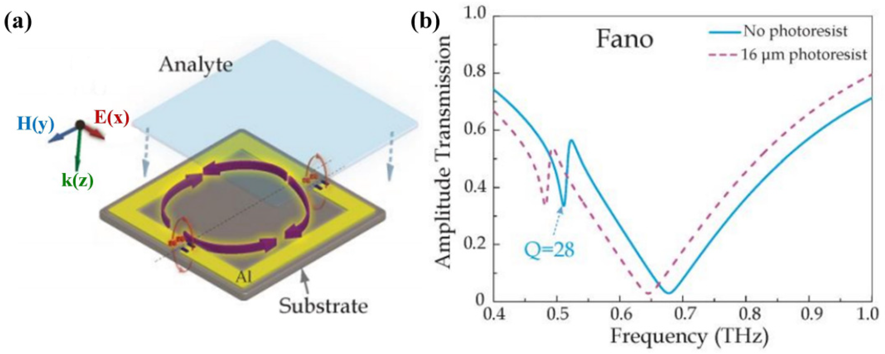
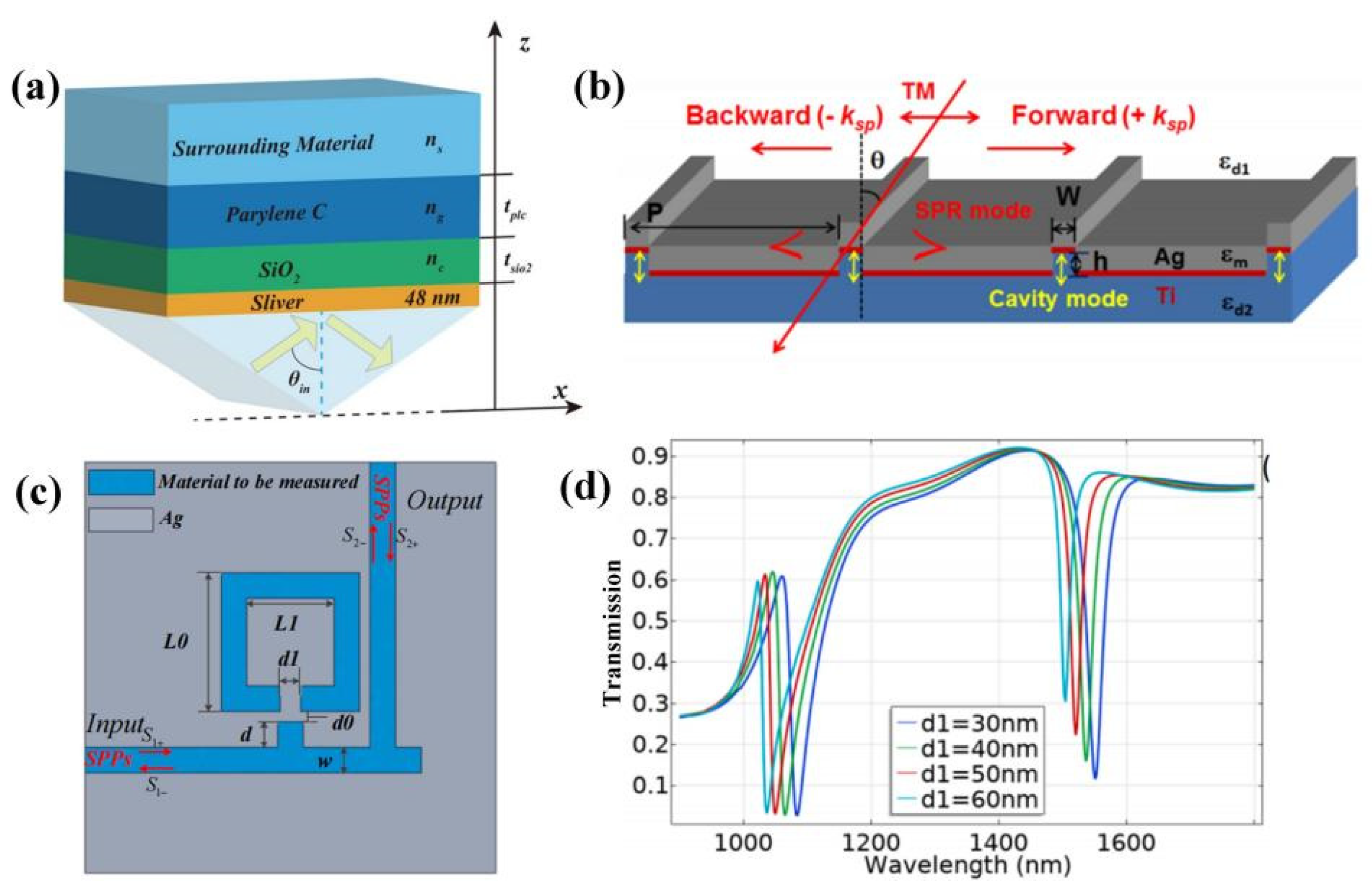
Fano Resonance and Sensors Based on Grating and Metal–Insulator–Metal Structures

Kretschmann configuration and metal grating structure
A prism–metal–dielectric–dielectric–analyte multilayer configuration is a typical Kretschmann configuration. It is found that the transmission profile of a multilayer configuration can be Fano–type [96,97,98,99], as shown in Figure 6a. A prism is used for phase matching, the metal layer leads to the deepest and narrowest SPR mode, and other layers support planar waveguide (PWG) mode. The coupling effects result in Fano resonance. However, the three–dimensional (3D) multilayer Fano resonance structure is excited by the prism, which is difficult to be integrated. The coupled waveguide grating structure is an effective strategy to achieve Fano resonance. In 1D metal grating structures, the metal and dielectric surfaces support the SPR mode, coupled near–field to the cavity mode supported in the cavity, and the transmission curve exhibits a Fano–type profile [100,101]. The 1D metal grating structure is shown in Figure 6b. Compared with the traditional SPR sensor, the SPR sensor based on a nano–grating structure has the advantages of no prism excitation, simple measurement, small detection volume and easy integration, as well as the ease of achieving multiple detection.
Plasmonic metal–insulator–metal waveguide–based Fano resonance
SPPs can break the diffraction limit and provide greater energy in the EM field. SPPs can be easily generated using metal–insulator–metal (MIM) waveguides. When the incident light hits the metal surface, if the wave vector of the incident light matches the SPP, the SPP is generated in the waveguide through the direct coupling of light. A narrowband resonant structure, such as a resonant ring, a stub, etc., is loaded near the MIM waveguide [102,103,104,105,106,107,108]. The SPP mode in the waveguide is coupled to the resonator, and the mode in the resonator interferes with the transmission mode of the MIM waveguide to generate single or multiple Fano resonances with high Q factor Fano resonance, as shown in Figure 6c,d. The MIM waveguide can be used to confine these light waves to the deep subwavelength scale, so the Fano resonance has a small loss and the resulting asymmetric line has a large slope. For these reasons, the Fano sensor formed by an MIM structure has higher sensitivity. The Fano resonance based on the plasmonic MIM cavity structure provides the possibility for the further development of photonic–integrated circuits. For example, a Fano sensor system was formed by a branched, semi–closed, T–shaped waveguide and a splitting square ring resonator [109]. When the incident light excited the MIM waveguide structure, the energy of the magnetic field was coupled to the resonator. Two different resonant modes were formed in the resonator and coupled to the branched, semi–closed waveguide. At wavelengths of 1060 nm and 1528 nm, the magnetic field distribution in the square ring resonator was opposite to that in the semi–closed, T–shaped waveguide. As a result, the near–field coupling led to destructive interference, generating asymmetric Fano resonances. Then, the sensing performance of the proposed structure was investigated by filling the square annular cavity and T–waveguide with different RI fluids. The waveguide and resonant structures that form the MIM Fano sensor are diverse, and the same method was used to design an MIM waveguide sensor with high sensitivity [110]. The high sensitivity of each mode of the sensor designed based on the MIM structure waveguide could reach 2600 nm/RIU and 1200 nm/RIU.

Fano Sensors Based on Single Resonant Structures

The shape of the resonant line of the traditional microdisk or microsphere resonator is symmetric with its resonant wavelength, and the mode of the structure is Lorentz resonance in the symmetric form. However, when a partial reflection element is introduced into the coupled waveguide, the phase of the propagating wave will be disturbed by the backpropagating wave introduced by the increased partial reflection element, resulting in complex interference [111], as shown in Figure 7a,b. This interference produces a sharp asymmetric Fano resonant line shape with a greatly increased slope between zero and pole transmission compared to a conventional microring. In addition, if the Q value of the resonator is increased and the slope of the resonance is increased, the sensitivity will be further improved. Using the same method, partial reflection element waveguides were replaced by T–shaped waveguides [112]. A T–shaped waveguide coupled with a microring resonator (MRR) generates Fano resonance at all resonance modes. Using two asymmetric structures to generate Fano resonance in biosensing, the structure consists of embedded high–Q–factor resonators. The mode number of the two micorings affects the Fano resonance line shape. The reversed Fano resonance occurs when the difference in the mode number is an odd number, whose line shape exhibits a much larger slope than the conventional Fano line shape [113]. The conventional Fano line shapes are formed when the difference in the mode number is an even number. Sharply asymmetric alignment greatly improves slope sensitivity. The resonant wavelength of the microring resonator depends on the effective RI of the waveguide mode or the biomolecules attached to its surface, or is influenced by the RI change in the surrounding environment as the waveguide envelope. Based on this, an experiment was performed to detect the concentration of glucose in an aqueous solution by using a fabricated thin polystyrene (PS) microring resonator. The minimum detectable concentration change for the glucose solution was 0.024%, or 24 mg/dL [111]. From the above summary, it is difficult to further integrate metal nanoparticles or metal arrays with on–chip photonic–integrated circuits. However, plasmonic–waveguide cavity–based sensors have unique advantages in terms of high performance, miniaturization, robustness and scalability, and they have excellent development prospects.

3.2.3. Fano Resonance Based on Nanoporous Gold and Its Sensing Applications

Nanoporous gold (NPG) is generated by the corrosion of an alloy of Au and a less noble metal, such as Ag or Cu, which is a three−dimensional bicontinuous porous network of interconnected ligaments formed by a self–organization process [114]. NPG is a promising sensing material for plasmonic platforms due to its advantages in terms of detection sensitivity and reaction efficiency. Due to the near−field enhancement of nanoporous gold, the confluence effect of improved quantum yield and excitation of fluorophores leads to a large fluorescence enhancement [115,116]. A fabricated 3D NPG membrane was firstly applied to biosensing [117]. Then, a 2D NPG structure was used for non–enzymatic glucose biosensing [118]. However, the pore size was much smaller than the wavelength of light, and nanoporous gold in the form of semi–infinite thin films exhibit weak plasmonic extinction and little tenability, which can be overcome by creating nanoporous gold in the form of disks with subwavelength diameter and sub–100 nm thickness [119]. Unlike NPG films, which exhibit weak light–matter interactions and limited tunability, periodic modulation of the NPG carrier surface could also support SPPs and LSPs [120]. The in–plane and out–of–plane LSPs modes on the NPG structure are related to the external shape of the nanoparticle, and these resonant frequencies depend on the diameter and distance of the disk. NPG disks feature a large specific surface area due to their internal nanoporous network and contain numerous plasmonic hot–spots throughout the internal volume, which enable high sensitivity to ambient index changes [121,122,123,124,125]. A label–free small–molecule sensor on nanoporous gold disks using surface–enhanced Raman spectroscopy (SERS) was reported. Due to the unique topological stabilized guaninequadruplex (G4) structure, target molecules were selectively captured by the surface of the NPG disk, where the minimum detectable concentration of conjugated exogenous molecules of non–double helix DNA nanostructures could reach 50 pM [124]. Then, the LOD of a nanoporous gold array (NPGA) sensor reached up to 10−10 IU [125]. Extraordinary transmission (EOT) supported by hole arrays [126] showed the line shape spectra of Fano resonance. Due to the spectrally destructive and constructive interference generated by the resonant interactions between SPPs and LSPs, Fano resonance EOT has shown a highly asymmetric transmission profile [127]. A schematic diagram of the experimental setup for biomolecular detection based on such a structure is shown in Figure 8a, and experimentally measured transmission spectra with different tested materials are shown in Figure 8b. The Fano resonance EOT signal is very sensitive to small changes in the local dielectric environment. The sensitivity of the transmission peak and dip is ~53 nm/RIU and ~32 nm/RIU, respectively, as shown in Figure 8c. Naked–eye detection of protein monolayers can be realized based on NHA nanostructures, and the FOM is up to 162 and the refractive index sensitivity is up to 717 nm/RIU, when using the light transmission phenomena of the sub–radiant dark mode with a high quality factor (Qsolution~200) [128]. Recently, EOT–based RI sensors have achieved high sensitivity of up to 1200.6 nm/RIU and a high FOM up to 279.2 [129].
A summary of the reported Fano resonant sensors is provided in Table 1. The sensors in Table 1 could be categorized into three types. The first type includes sensors with high sensitivity but a very low Q factor. As for periodic metamaterial sensors, the sensitivity is often extremely high, up to ~104 nm/RIU. However, due to the radiation and non–radiation losses in metamaterial structures, their Q factors are very low [64,130,131,132]. The second category consists of structures with high sensitivity but limited FOM. As for Fano resonance, FOM is defined as the product of the Q factor and resonance intensity (I). Normally, an optimized high Q factor can be obtained by tuning the structural asymmetry, while the resonance intensity is low, which limits the maximum FOM [133]. Hence, for sensors based on Fano resonance, it is necessary to optimize the structural parameters to obtain an appropriate Q factor and I values for an optimized FOM. The third type comprises active Fano resonance sensors, which can compensate for different losses. Although the sensitivity of the sensors in Refs. [64,67,71] is effectively improved, their FOM could be further improved. Compared with the passive Fano resonance sensors [70,72,88,100,112], active Fano structures simultaneously improve the resonance intensity and Q factor of the Fano resonance [121], which often results in higher sensitivity [90,91]. The final work is based on the EOT Fano resonance structures. It not only reduces the sensing time of measurement, but also improves the sensitivity through the contact area between molecules and NPG [127,128,129].

4. Exceptional Point

4.1. Theory of Exceptional Point

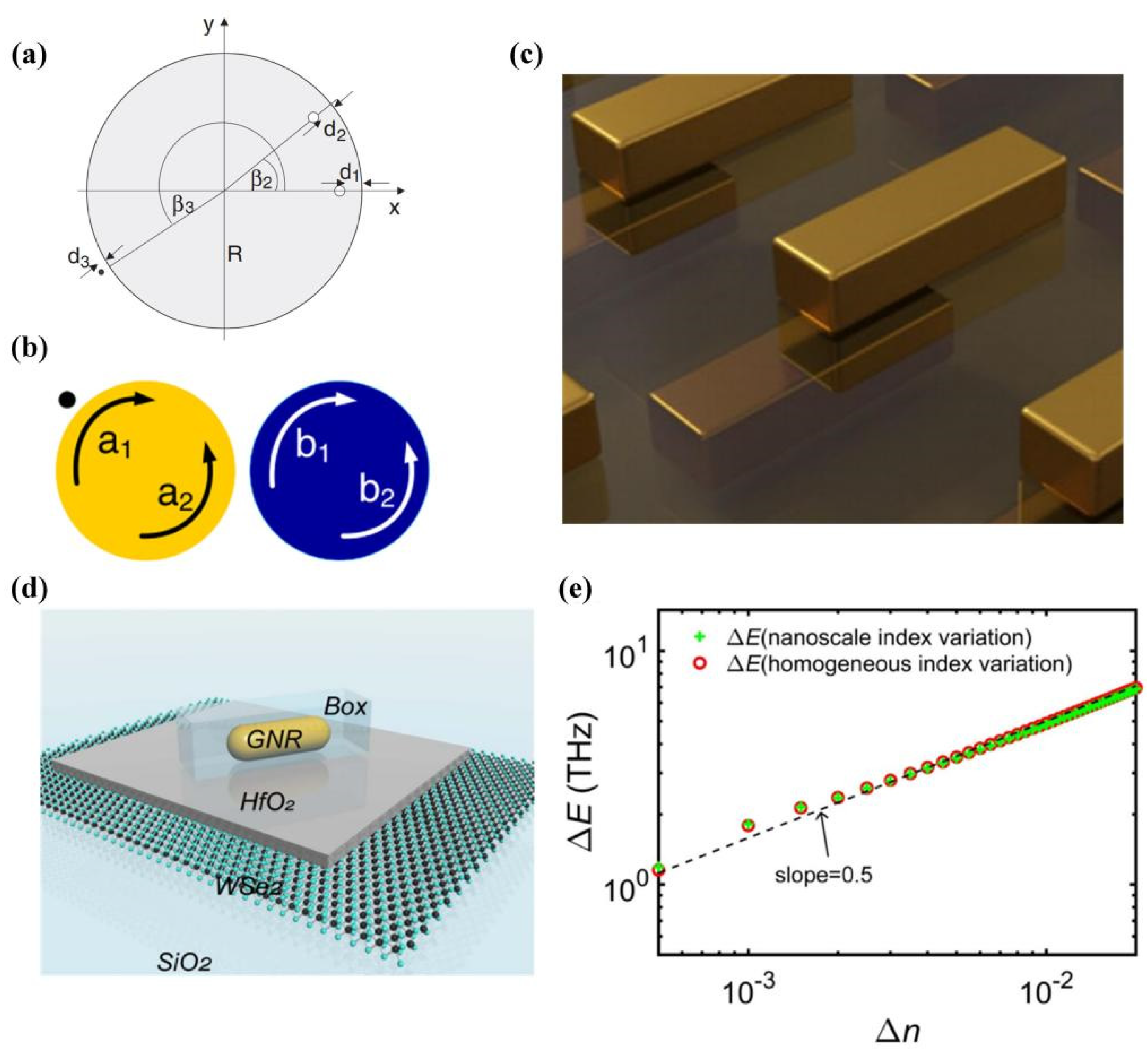
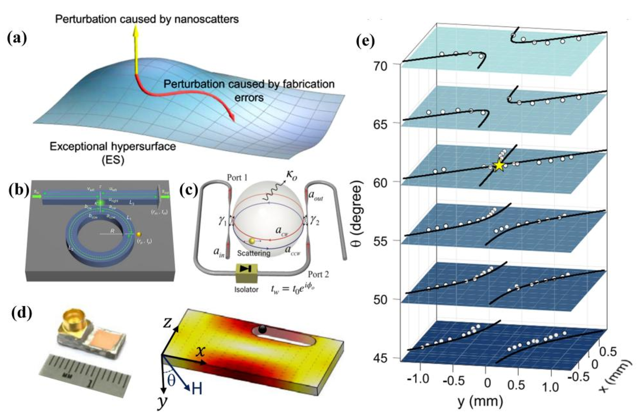
4.1.1. Design of EP Resonator

Owing to the formal equivalence between the Schrödinger wave equation and the paraxial EM wave equation [134], a non–Hermitian Hamiltonian can be achieved by spatially modulating dissipation and amplification in a wide range of optical and photonic systems. Spectrum–splitting sensors are generally implemented based on coupled systems. Optical whispering gallery microcavities (WGM) have the CW and CCW mode. When CW and CCW in the resonator are unidirectionally coupled, the system has only one special resonant point, namely the EP. The system is coupled by a silicon dioxide microring cavity and a fiber conical waveguide (used for the internal and external coupling of light) [43]. The relative positions of the two scattering particles near the ring cavity are adjusted to enable the unidirectional coupling of CW and CCW to achieve the EP. Another scattering particle is added to the system as a disturbance, causing the EP to split. The real and imaginary parts of the eigenfrequency at the EP are degenerated, but the system introduces perturbations, and the real and imaginary parts of the system split simultaneously. The transmission curve of the EP only has one resonant point, while there are two resonant points when the EP splits. An EP sensor was demonstrated in experiments, which highlighted the enhancement effect regarding the sensitivity. WGM provides a research platform for studying EP [44,135,136]. The properties of equivalent Hamiltonian operators are described with the help of coupled mode theory (CMT). Assume that the gain and loss of each component in the system are γ 1 and γ 2 , respectively; the resonant frequency is ω 1 and ω 2 , respectively; and the mode coefficient is a 1 and a 2 , where a 1 , 2 = a 1 , 2 e i ( ω 1 , 2 i γ 1 , 2 ) t , and the coupling coefficient is κ . According to the CMT,
d a 1 d t = i ω 1 a 1 γ 1 a 1 i κ a 2
d a 2 d t = i ω 2 a 2 γ 2 a 2 i κ a 1
In the form of the Schrödinger equation i ψ t = H ^ ψ , the Hamiltonian operator of the system is obtained:
H ^ = [ ω 1 i γ 1 κ κ ω 2 i γ 2 ]
The unitary matrix is introduced, M = [ 1 2 i 2 1 2 i 2 ] . The equivalent Hamiltonian operator of the system is obtained by unitary transformation H ˜ = M H ^ M [137]:
H ˜ = [ ω 0 A 0 B 0 ω 0 ]
where ω 0 = ( ω 1 + ω 2 ) i ( γ 1 + γ 2 ) 2 ,   A 0 = ( ω 1 ω 2 ) i ( γ 1 γ 2 ) 2 i κ , B 0 = ( ω 1 ω 2 ) i ( γ 1 γ 2 ) 2 + i κ . If A 0 = 0 and B 0 0 or B 0 = 0 , and A 0 0 , the system can be set to the EP state. At the EP, the system must meet the following requirements:
ω 1 ω 2 = 0
4 κ 2 ( γ 1 γ 2 ) 2 = 0
2 κ + ( γ 1 γ 2 ) = 0   or   2 κ ( γ 1 γ 2 ) = 0
In other words, the resonant frequencies of the two modes are the same, and the coupling coefficient is linear with the loss difference. By analyzing the above formula, at EP, the equivalent Hamiltonian B 0 = 0 , which easily leads to κ = γ 1 γ 2 2 ; we insert it in A 0 , and obtain A 0 = i ( γ 1 γ 2 ) . The results show that at the EP, the system meets the following conditions: the resonant frequencies of the two resonant modes are the same and the loss difference cannot be the same. The loss difference affects the performance of sensors based on the EP.

4.1.2. Improved Sensing Performance of EP Sensors

For the two–mode component coupled system, assuming that the change in a physical parameter of the object to be measured is the perturbation of the sensor, the Hamiltonian operator of the sensing system is H ^ = H ^ 0 + ε H ^ 1 , where ε represents the perturbation intensity, H ^ 0 represents the Hamiltonian operator of the system without perturbation, and H ^ 1 represents the perturbation part of the Hamiltonian operator,
H ^ 1 = [ 0 A 1 B 1 0 ]
where A 1 and B 1 are the coupling coefficients between two basis vectors. The total system eigenvalues are E 1 = E 0 + ε A 0 B 0 + ε ( A 0 B 1 + A 1 B 0 ) + ε 2 A 1 B 1 and E 2 = E 0 ε A 0 B 0 + ε ( A 0 B 1 + A 1 B 0 ) + ε 2 A 1 B 1 . The system eigenvalue splitting quantity is
Δ E = ε A 0 B 0 + ε ( A 0 B 1 + A 1 B 0 ) + ε 2 A 1 B 1
When A 0 = 0 or B 0 = 0 , B 1 0 and ε is small enough, Δ E is proportional to ε . It can be seen that the EP–based sensor can effectively enhance the sensor performance in the case of small perturbations.

4.2. Development of EP and Sensors Based on EP

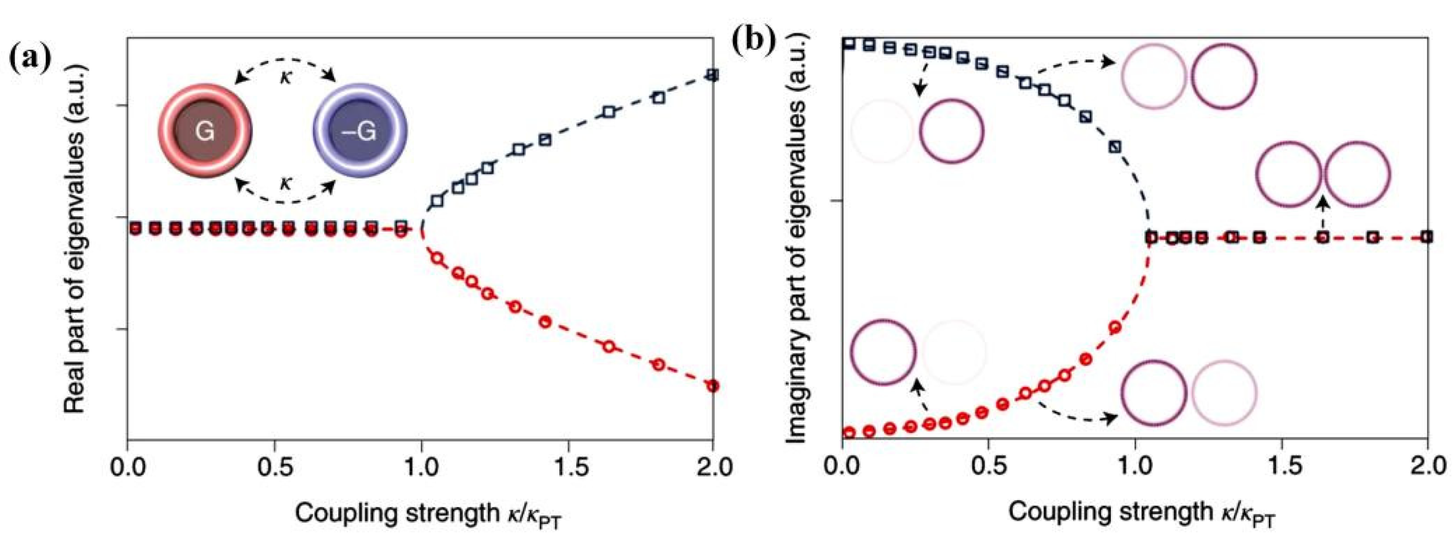
4.2.1. Exceptional Point in Passive Systems

Regarding photonic systems, the EP has been studied in many systems. Structures commonly used to implement the EP include single–microcavity systems of WGM [44,45,46], waveguides [138] and two–component coupled systems [51,137,139]. In the WGM microcavity structure, the WGM utilizes total internal reflection to localize light in the cavity, which has a very high Q factor and is helpful to realize high–sensitivity sensing. Applications include nanoparticle detection [140], temperature sensing [141], RI sensing [142], optical gyroscopes [143] and graphene biochemistry [144]. Traditional WGM microcavity detection of a single nanoparticle depends on diabolic point (DP) degeneracy, and its frequency splitting quantity is related to the particle size. In 2016, Wiersig presented a paper on an EP–based single particle detection strong sensor, theoretically proving the sensitivity of the EP for weak perturbation detection [145]. Since then, the EP sensor has been gradually applied.
In the field of optics, the initial research based on EP sensing has been implemented based on passive systems. In addition to multiple particles interacting with the WGM resonator to modulate the EP [44], two coupled WGM resonant rings can also be used to achieve unidirectional wave transmission and generate the EP [136,146]. Figure 9a shows a WGM resonator that excites the EP, and Figure 9b shows a two–coupled WGM resonator. In Ref. [146], the fiber Bragg grating (FBG) was introduced as a tuning part (which can isolate the influence of acoustic waves and maintain a more stable mode splitting signal) to keep the system in the EP. In addition, by introducing a resonant ring loaded with an isolator, the CW and CCW of the resonator generate non–reciprocal coupling (loop asymmetry loss). The different intracavity power causes a local temperature change at the FBG, which causes the system frequency to split. The EP is sensitive to perturbation only within a certain range, i.e., it holds at time κ 2 = Δ γ / 2 . The EP concept has also been widely introduced into other traditional fields. An EP sensor based on the resonant optical tunneling effect (ROTE) was used for low–concentration carcinoembryonic antigen (CEA) detection, with a sensitivity of 17,120 nm/IP [49]. The sensor is a passive non–Hermitian EP system, which has the advantage of avoiding experimental complexity and instability. The sensing system uses the common method of traditional microwave biosensors, namely the antigen–antibody reaction, which leads to an RI change and then spectrum splitting. However, passive sensing systems are often limited by their low Q factor. The system frequency splitting is very small, which makes the splitting arguably poor.
In plasmonic nanostructures, plasmons are collective oscillations of free electrons coupled to photons, which shrink the wavelength of light to the scale of electrons and molecules. The observation of EP is limited to wavelength–scale systems affected by the diffraction limit. The EP can be obtained by spatial symmetry breaking. The plasmonic EP is formed based on the hybridization of the detuning resonance in the multilayer plasmonic structure to achieve the critical complex coupling rate between the nanoantenna arrays, leading to the simultaneous degeneracy of the resonance frequency and the loss rate [147], as shown in Figure 9c. The EP system has a sensitivity of 4821 nm/RIU. In addition, in the plasmonic–exciton hybrid system, the plasmonic excitation subsystem consists of a gold nanorod (GNR) and the monolayer WSe2, as shown in Figure 9d [50]. By controlling the geometric parameters of the hybrid system, the EP combining the resonance frequency and the loss rate of the hybrid system is obtained. Changing the effective RI around the GNR can also modify the coupling between the plasmons and exciton modes to achieve highly sensitive sensors at the nanoscale. The variation in frequency splitting with RI is shown in Figure 9e.

4.2.2. Exceptional Surface
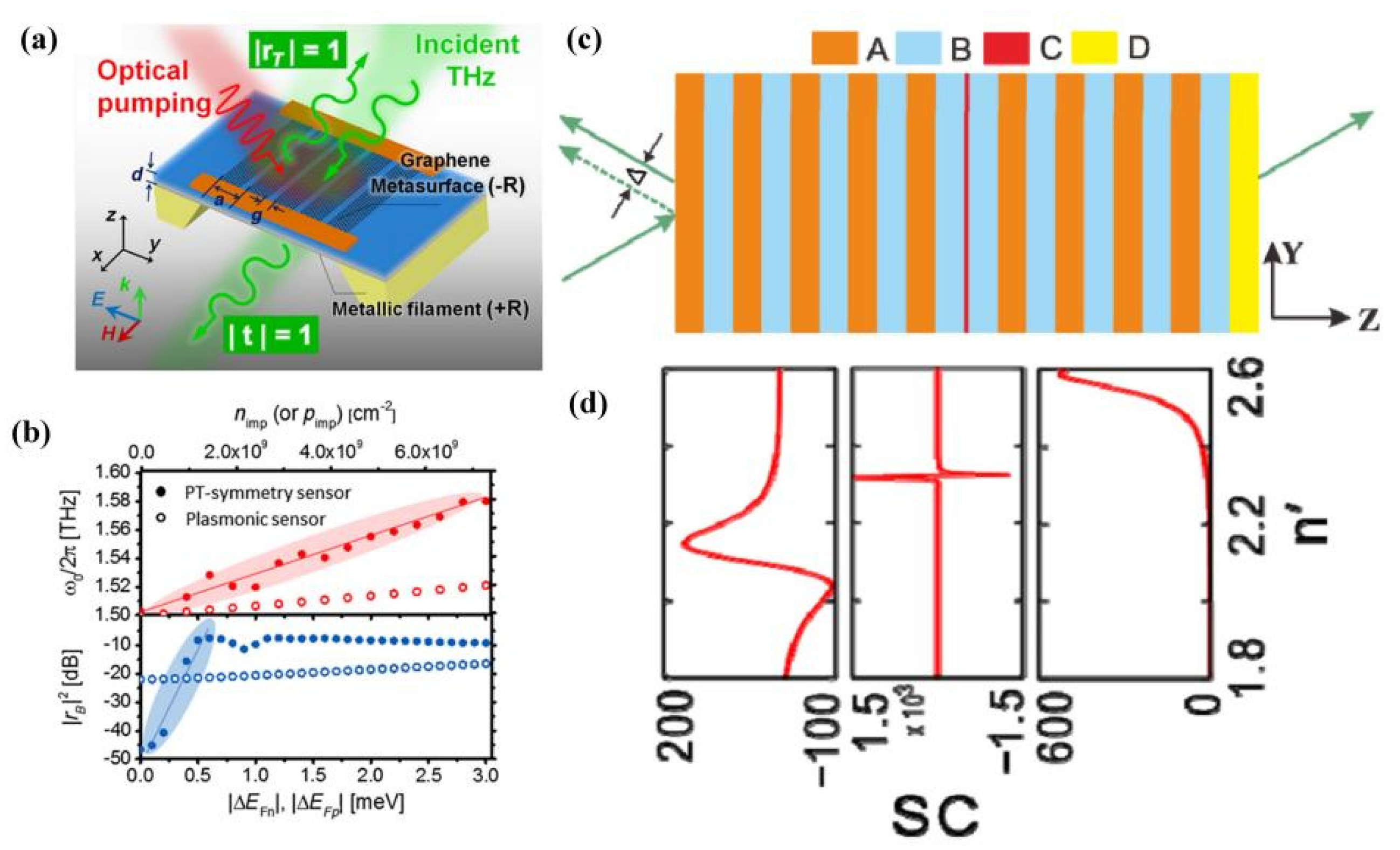
In order to improve the robustness of the system, the exceptional surface (ES) is proposed, which is a special surface formed by an infinite number of Eps. The ES system has the advantages of both robustness and high sensitivity [148,149,150,151,152,153]. The concept map of ES is shown in Figure 10a and shows that multiple unwanted disturbances (such as fabrication errors) force the EP to move along the ES, and the system reaches an EP state under the desired disturbance. In a system consisting of an optical waveguide and WGM [148,150], a microring resonator is coupled to a waveguide with an end mirror, and tuning of the intensity and phase of the specular reflection enables unidirectional coupling between CW and CCW modes to induce EP, as shown in Figure 10b. Since the formed eigenfrequencies do not split for all frequencies, loss and coupling, regardless of how these parameters are changed (machining errors, experimental uncertainties), the system will be in EP and an ES will be formed. When both sides of the tapered fiber are coupled with silicon microspheres several times [151,153], the isolator is loaded on the fiber at the same time, so that the output of port 1 is reused as the input of port 2, and vice versa. This unidirectional coupling between CW and CCW produces ES. The unidirectional coupling ES structure is shown in Figure 10c. In these ES systems, when a state that breaks this unidirectional coupling (the unidirectional coupling between CW and CCW) is introduced, the intrinsic frequency of the system splits. In the WGM system, the unidirectional coupling of the manufacturing system is used to place the system in ES. Another common method is to introduce more tunable parameters [139] to cause ES to appear in the system. Figure 10d shows the magnon polariton system with multiple tuning parameters. The 3D structure consists of a microwave cavity and a magnonic cavity ES can be tuned in multiple dimensions simultaneously to coalesce into an exceptional saddle point (ESP). Figure 10e shows that a degenerate EP can be obtained by adjusting the other three parameters when the applied magnetic field strength is fixed.

4.2.3. Active EP

The EP occurs in non–Hermitian systems. Several studies have shown that the EP can still exist based on a parity−time (PT)–symmetric system. In quantum mechanics, all observable physical quantities satisfy Hermitian symmetry and their eigenvalues are real numbers. It was not until 1998 that Bender and Boteecher discovered that if parity time (PT) symmetry is satisfied (physical process returns to its initial state under spatio−temporal inversion), the eigenvalues of non−Hermitian operators may also be real numbers [154]. Operators are usually used to represent mechanical quantities, and Hamiltonian operators represent the total energy in the system, which should satisfy the PT symmetry condition:
H ^ P ^ T ^ = P ^ T ^ H ^
The P operator represents the spatial inversion transformation, and the effect is to change the spatial operator x ^ and momentum operator p ^ , x ^ x ^ ,   p ^ p ^ , while T represents the temporal inversion transformation, and the effect is to change the momentum operator p ^ and complex units i , x ^ x ^ ,   p ^ p ^ , i ^ i ^ . Suppose that there exists a simple Hamiltonian H = p 2 / 2 + V ( x ) , where x is the space coordinate, and V ( x ) is the potential function of the system. After P operator and T operator operation on the Hamiltonian operator, H P T = p 2 / 2 + V ( x ) and P T H = p 2 / 2 + V * ( x ) are obtained. If PT is symmetric, V ( x ) = V * ( x ) is obtained. In other words, the potential function satisfying the condition of PT symmetry must satisfy even symmetry in the real part and odd symmetry in the imaginary part. In optical systems, gain and loss media are introduced to regulate the real and imaginary parts of the RI. For PT–symmetric optical systems, the real part of the RI is an even function, and the imaginary part is a strange function. There is a threshold in the parameters of a PT–symmetric system beyond which the system spontaneously breaks the symmetry and the eigenvalue becomes a pure complex number. This threshold is called the phase transition point, or EP. Figure 11a,b show the change process of the real and imaginary parts of the eigenvalues of the PT–symmetric system with the coupling strength [155]. The spectrum of PT symmetry presents real numbers, which lays the foundation for the development of EP. PT is also an important means to realize EP. EP can be implemented in conjunction with other physical phenomena, such as Fano resonances in graphene–doped multilayer metamaterials, when the narrowband discrete states undergo destructive interference with the wideband continuum, without changing the permittivity or structural parameters of the system [156]. The Fano–type reflection was adjusted by adjusting the chemical potential of graphene to find the zero reflection point. Fano resonances can exhibit an optical EP: the system has non–Hermitian properties, where the eigenvalues and eigenvectors of the Hamiltonian function are simultaneously degenerate. Near the EP point, the transmission and reflection of light in the metamaterials undergo drastic changes upon changing the incident wavelength and the chemical potential of graphene in the parameter space. Taking advantage of the high tunability of graphene, Fano resonance can be applied to graphene metamaterials to achieve EP. By adjusting the conductance of graphene, the peak position and value of the Fano–type reflection can be changed. It has been proven theoretically that the active sensor based on PT symmetry can provide higher sensitivity than the traditional passive sensor [157,158]. PT symmetry can improve the Q factor of the resonator, which is conducive to improving the sensitivity and resolution of the sensor.
A PT–symmetric system based on a pair of metasurfaces with balanced gain–loss distributions is proposed, as shown in Figure 12a. The structure is based on the combination of PT symmetry and the tunable conductivity of graphene, and it uses the pairing of active graphene and nickel–chromium metal resistance wire to design the PT symmetry impedance distribution structure. Two different approaches have been investigated for such systems: closed–loop analysis of admittance or impedance matrices (analogous to the effective Hamiltonian [144]) and characteristic problems for scattering matrices. Unidirectional zero–reflected EP resulting from sharp resonances associated with EP or coherent perfectly absorbing laser spots (CPAL) may result in significantly modulated the scattering responses or resonance shifts. If the Fermi level of graphene is taken as the perturbation of the sensor, it can be seen that the structure is sensitive to the change in the perturbation, as shown in Figure 12b. For the broad–spectrum analysis, the PT–symmetric sensor exhibits a high sensitivity of 1.15 GHz/μm2, which is also significantly greater than that of the graphene plasmonic sensor. PT symmetry can also be implemented in high–order EP sensing systems. A temperature sensor based on third–order EP consists of a ternary coupled microloop consisting of a loss cavity, a neutral cavity, and an active cavity [141]. A heating element is placed under each microcavity to fine–tune the resonant frequency and introduce thermal perturbation, so that the imaginary and real parts of the RI are independently controlled to establish third–order singularities. Figure 13c is the curve of the frequency splitting amount as a function of the disturbance intensity ε I 2 , which proves that the frequency splitting amount at the third–order EP is proportional to the cube root of perturbation. Compared with the traditional single microcavity, the sensitivity is enhanced by 23 times. The change in RI can also lead to the spatial displacement of the reflected beam at the boundaries of different RI media, which is called Goos–Hanchen (GH) displacement [159]. The multilayer dielectric RI sensor is shown in Figure 12c; it achieves EP under the parameter adjustment of the incident angle and the real part of the D–layer RI. GH displacement is direction–first and sensitive to small RI changes. Figure 12d shows the curve of the sensitivity corresponding to different incident angles θ as a function of the real part of the RI of layer D. It can be seen that the sensitivity near the EP is up to 103 times the wavelength. A quasi–PT–symmetric layered resonator coupling system is composed of four identical metal films (M), in which the metal films are the gain layer (G), loss layer (L) and air layer (A) [142]. An isolator pole with large transmittance is introduced into this structure. Since the polar mode is generated by mode coupling through the cavity, the transmittance of the structure is very sensitive to the RI of the cavity and the background air. The sensor detects the RI and gas concentration of mixed air by measuring the transmittance height at the pole. The maximum sensitivities of −∆T/(Tp) are 668 and 76.6 for benzene and for methane, respectively. Some of the applications of EP sensors are summarized in Table 2. Recently, the sensitivity of a refractive index sensor reached up to 100 THz/RIU [50]. The prominent advantage of EP sensors is its sensitivity to small or minute perturbations, which can include a minor change in temperature [141], angle [160], area [144], RI [50,147,161], etc., so it has also a very wide range of applications.

5. Outlook of Fano and EP Sensors

5.1. Fano Sensors

Theoretically, the Fano resonance is generated by the interference between the non–radiative dark mode and the radiative bright mode. Different structures are used to manipulate Fano resonances, as well as local field enhancement. Most work is achieved by breaking the symmetry of the structure. In general, the formation of the Fano resonance depends on the tuning of the physical characteristics of the structure. Once the structure is designed, it cannot be changed, and the resonance characteristics cannot be changed either. However, the actively tuned Fano resonance is not only convenient to find the optimal structure, but also can reduce the experimental cost. Some studies have found that Fano resonance based on artificial materials is not perfect. The Q of Fano resonance is inversely related to the resonance strength. For example, the Q of Fano resonance increases while the resonance strength decreases [162], as shown in Figure 13a,b. This limits the applications of Fano resonance sensors. Therefore, the actively tuned high–sensitivity Fano resonance sensor has excellent development prospects.
In summary, although higher sensitivity and FOM have been achieved based on Fano resonance sensors, there are still limitations. First, most Fano resonance sensors can only measure a single parameter, such as the refractive index. Secondly, most sensors are sensitive to the operation environment, and robustness and consistency are required. The self–reference Fano resonance sensor provides a strategy to solve this problem. Lastly, with the development of integrated circuits, the miniaturization of sensors is becoming increasingly necessary. Hence, compact multifunctional Fano resonance sensors with multiple channels, self–reference and on–chip integration capability are expected, which would provide more potential applications in the future.

5.2. EP Sensors

The advantage of EP is that it is sensitive to small perturbations, but it cannot distinguish whether the perturbations are caused by errors (experimental uncertainties, processing errors). The proposal of ES can solve this problem, but the formation of ES often needs to introduce more tunable degrees of freedom into the system. The approach is to increase the complexity of the system in exchange for stability. However, forming such a sensing system is not easy. Therefore, forming ES by simple means is the main exploration direction for the formation of a stable EP in the future.
In practice, the larger the loss difference, the wider the linewidth of the resonance, which makes the spectrum splitting difficult to observe. The magnitude of the frequency splitting factor determines whether the frequency splitting can be observed, which is defined as the ratio of half of the sum of the frequency splitting and the splitting resonance linewidths [45,46],
Q s p = 4 g γ s u m
where 2 g = | ω 1 ω 2 | is the frequency splitting and γ s u m is the sum of the linewidths of the resonance [140,163]. Figure 13c demonstrates that the frequency split in the experiment can be easily identified only when the value of Q s p is greater than 1, and the minimum value Q s p is reached at the EP. For loss–making systems, the linewidths of the intrinsic frequencies near the EP are so wide that frequency splitting cannot always be identified. Therefore, for a system with a large loss difference, even if the sensitivity is high, the frequency splitting may not be seen, affecting the sensing performance. PT asymmetry may overcome the drawbacks of the large linewidth of the resonance and enhance the sensitivity of sensors. However, it is required to balance the losses with the additional gain introduced for the PT–symmetric system. Furthermore, EP sensors based on PT–symmetric systems introduce additional unstable factors to the system, such as noise, which increases the complexity and cost of the system. The question of how to reduce the noise level to improve the sensitivity of EP sensors is a great challenge for future PT–symmetric sensors.
By reviewing the development status of EP sensing, it can be seen that both types of EP sensors based on ES and PT symmetry have increased the complexity of the system to obtain higher sensitivity for minute disturbances. There is a debate regarding whether higher sensitivity could be obtained when higher noise is considered. Hence, it is important to explore robust and stable EP sensors that do not affect the sensitivity in the future.

6. Conclusions

Different structures to achieve plasmonic Fano resonance and EP have been reviewed. Due to the field enhancement and steep asymmetric scattering profile of the plasmonic Fano resonance and the high sensitivity to the minute changes in EP, it has been shown that they are suitable for highly sensitive sensors. The degenerated state of the EP is extremely sensitive to perturbations and the changes in low–concentration detection substances, indicating important applications and good prospects for new sensors. The working principles, the latest work and the future trends of these plasmonic nanosensors and metasensors have been fully summarized. It has been concluded that Fano resonance sensors and EP sensors in plasmonic structures have higher sensitivity and wide applications.

Author Contributions

Conceptualization, Q.L. and Y.Z.; methodology, Q.L. and Y.Z.; writing—original draft preparation, Q.L.; X.W. and Y.Z.; review and editing, Q.L.; X.W. and Y.Z.; visualization, Q.L. and Y.Z. All authors have read and agreed to the published version of the manuscript.

Funding

This work is supported by the National Natural Science Foundation of China under Grant No. 61971469, by the Science and Technology Commission Shanghai Municipality under Grant No. 18ZR1413500, and in part by the Open Project Program of the State Key Laboratory of Millimeter Waves under Grant No. K202109.

Institutional Review Board Statement

Not applicable.

Informed Consent Statement

Not applicable.

Data Availability Statement

Not applicable.

Conflicts of Interest

The authors declare no conflict of interest.

References

  1. Brongersma, M.L.; Shalaev, V.M. The Case for Plasmonics. Science 2010, 328, 440–441. [Google Scholar] [CrossRef] [PubMed]
  2. Kelly, K.L.; Coronado, E.; Zhao, L.L.; Schatz, G.C. The Optical Properties of Metal Nanoparticles: The Influence of Size, Shape, and Dielectric Environment. J. Phys. Chem. B 2003, 107, 668–677. [Google Scholar] [CrossRef]
  3. Li, W.; Camargo, P.; Lu, X.; Xia, Y. Dimers of Silver Nanospheres: Facile Synthesis and Their Use as Hot Spots for Surface–Enhanced Raman Scattering. Nano Lett. 2008, 9, 485–490. [Google Scholar] [CrossRef]
  4. Nie, S.; Emory, S.R. Probing Single Molecules and Single Nanoparticles by Surface–Enhanced Raman Scattering. Science 1997, 275, 1102–1106. [Google Scholar] [CrossRef] [PubMed]
  5. Anker, J.N.; Hall, W.P.; Lyandres, O.; Shah, N.C.; Zhao, J.; Van Duyne, R.P. Biosensing with plasmonic nanosensors. Nature materials 2008, 7, 442–453. [Google Scholar] [CrossRef] [PubMed]
  6. Liu, N.; Weiss, T.; Mesch, M.; Langguth, L.; Eigenthaler, U.; Hirscher, M.; Sönnichsen, C.; Giessen, H. Planar Metamaterial Analogue of Electromagnetically Induced Transparency for Plasmonic Sensing. Nano Lett. 2009, 10, 1103–1107. [Google Scholar] [CrossRef] [PubMed]
  7. Kazuma, E.; Tatsuma, T. Localized surface plasmon resonance sensors based on wavelength–tunable spectral dips. Nanoscale 2013, 6, 2397–2405. [Google Scholar] [CrossRef]
  8. Chang, C.-Y.; Lin, H.-T.; Lai, M.-S.; Shieh, T.-Y.; Peng, C.-C.; Shih, M.-H.; Tung, Y.-C. Flexible Localized Surface Plasmon Resonance Sensor with Metal–Insulator–Metal Nanodisks on PDMS Substrate. Sci. Rep. 2018, 8, 11812. [Google Scholar] [CrossRef]
  9. Li, G.; Wang, Z.; Mao, X.; Zhang, Y.; Huo, X.; Liu, H.; Xu, S. Real–Time Two–Dimensional Mapping of Relative Local Surface Temperatures with a Thin–Film Sensor Array. Sensors 2016, 16, 977. [Google Scholar] [CrossRef]
  10. Lee, C.; Lawrie, B.; Pooser, R.; Lee, K.-G.; Rockstuhl, C.; Tame, M. Quantum Plasmonic Sensors. Chem. Rev. 2021, 121, 4743–4804. [Google Scholar] [CrossRef] [PubMed]
  11. Salomon, L.; Bassou, G.; Aourag, H.; Dufour, J.P.; de Fornel, F.; Carcenac, F.; Zayats, A.V. Local excitation of surface plasmon polaritons at discontinuities of a metal film: Theoretical analysis and optical near–field measurements. Phys. Rev. B 2002, 65, 125409. [Google Scholar] [CrossRef]
  12. Caballero, B.; García–Martín, A.; Cuevas, J.C. Hybrid Magnetoplasmonic Crystals Boost the Performance of Nanohole Arrays as Plasmonic Sensors. ACS Photonics 2016, 3, 203–208. [Google Scholar] [CrossRef]
  13. Diaz–Valencia, B.F.; Mejía–Salazar, J.R.; Oliveira, J.O.N.; Porras–Montenegro, N.; Albella, P. Enhanced Transverse Magneto–Optical Kerr Effect in Magnetoplasmonic Crystals for the Design of Highly Sensitive Plasmonic (Bio)sensing Platforms. ACS Omega 2017, 2, 7682–7685. [Google Scholar] [CrossRef] [PubMed]
  14. Vassant, S.; Archambault, A.; Marquier, F.; Pardo, F.; Gennser, U.; Cavanna, A.; Pelouard, J.-L.; Greffet, J.-J. Epsilon–Near–Zero Mode for Active Optoelectronic Devices. Phys. Rev. Lett. 2012, 109, 237401. [Google Scholar] [CrossRef]
  15. Traviss, D.; Bruck, R.; Mills, B.; Abb, M.; Muskens, O. Ultrafast plasmonics using transparent conductive oxide hybrids in the epsilon–near–zero regime. Appl. Phys. Lett. 2013, 102, 121112. [Google Scholar] [CrossRef]
  16. Padilla, W.J.; Basov, D.N.; Smith, D.R. Negative refractive index metamaterials. Mater. Today 2006, 9, 28–35. [Google Scholar] [CrossRef]
  17. Smith, D.R.; Pendry, J.B.; Wiltshire, M.C.K. Metamaterials and Negative Refractive Index. Science 2004, 305, 788–792. [Google Scholar] [CrossRef] [PubMed]
  18. Rasad, A.; Yudistira, H.T.; Qalbina, F.; Saputro, A.G.; Faisal, A. Multilayer flexible metamaterials based on circular shape with negative refractive index at microwave spectrum. Sens. Actuators A Phys. 2021, 332, 113208. [Google Scholar] [CrossRef]
  19. Abdulkarim, Y.I.; Deng, L.; Luo, H.; Huang, S.; Karaaslan, M.; Altıntaş, O.; Bakır, M.; Muhammadsharif, F.F.; N. Awl, H.; Sabah, C.; et al. Design and study of a metamaterial based sensor for the application of liquid chemicals detection. J. Mater. Res. Technol. 2020, 9, 10291–10304. [Google Scholar] [CrossRef]
  20. Karawdeniya, B.I.; Damry, A.M.; Murugappan, K.; Manjunath, S.; Bandara, Y.M.N.D.Y.; Jackson, C.J.; Tricoli, A.; Neshev, D. Surface Functionalization and Texturing of Optical Metasurfaces for Sensing Applications. Chem. Rev. 2022, 107, 2411–2502. [Google Scholar] [CrossRef] [PubMed]
  21. Miroshnichenko, A.E.; Flach, S.; Kivshar, Y.S. Fano resonances in nanoscale structures. Rev. Mod. Phys. 2010, 82, 2257–2298. [Google Scholar] [CrossRef]
  22. Luk'Yanchuk, B.; Zheludev, N.I.; Maier, S.A.; Halas, N.J.; Nordlander, P.; Giessen, H.; Chong, C.T. The Fano resonance in plasmonic nanostructures and metamaterials. Nat. Mater. 2010, 9, 707–715. [Google Scholar] [CrossRef] [PubMed]
  23. Rahmani, M.; Luk'Yanchuk, B.; Hong, M. Fano resonance in novel plasmonic nanostructures. Laser Photonics Rev. 2012, 7, 329–349. [Google Scholar] [CrossRef]
  24. Limonov, M.F.; Rybin, M.; Poddubny, A.; Kivshar, Y.S. Fano resonances in photonics. Nat. Photonics 2017, 11, 543–554. [Google Scholar] [CrossRef]
  25. Athe, P.; Srivastava, S.; Thapa, K.B. Electromagnetically induced reflectance and Fano resonance in one dimensional superconducting photonic crystal. Phys. C Supercond. 2018, 547, 36–40. [Google Scholar] [CrossRef]
  26. Liu, H.; Li, G.X.; Li, K.F.; Chen, S.M.; Zhu, S.N.; Chan, C.T.; Cheah, K.W. Linear and nonlinear Fano resonance on two–dimensional magnetic metamaterials. Phy. Rev. 2011, 84, 235437.1–235437.6. [Google Scholar] [CrossRef]
  27. Mun, S.-E.; Yun, H.; Choi, C.; Kim, S.-J.; Lee, B. Enhancement and Switching of Fano Resonance in Metamaterial. Adv. Opt. Mater. 2018, 6, 1800545. [Google Scholar] [CrossRef]
  28. Mun, S.-E.; Choi, C.; Hong, J.; Lee, B. Broadband wavelength demultiplexer using Fano–resonant metasurface. Nanophotonics 2020, 9, 1015–1022. [Google Scholar] [CrossRef]
  29. Chen, L.; Xu, N.; Singh, L.; Cui, T.; Singh, R.; Zhu, Y.; Zhang, W. Defect-Induced Fano Resonances in Corrugated Plasmonic Metamaterials. Adv. Opt. Mater. 2017, 5, 1600960. [Google Scholar] [CrossRef]
  30. Lassiter, J.B.; Sobhani, H.; Fan, J.A.; Kundu, J.; Capasso, F.; Nordlander, P.; Halas, N.J. Fano Resonances in Plasmonic Nanoclusters: Geometrical and Chemical Tunability. Nano Lett. 2010, 10, 3184–3189. [Google Scholar] [CrossRef]
  31. Li, W.; Su, Y.; Zhai, X.; Shang, X.; Xia, S.; Wang, L. High– $Q$ Multiple Fano Resonances Sensor in Single Dark Mode Metamaterial Waveguide Structure. IEEE Photonics Technol. Lett. 2018, 30, 2068–2071. [Google Scholar] [CrossRef]
  32. Wang, C.L.; Wang, Y.Q.; Hu, H.; Liu, D.J.; Gao, D.L.; Gao, L. Reconfigurable sensor and nanoantenna by graphene–tuned Fano resonance. Opt. Express 2019, 27, 35925–35934. [Google Scholar] [CrossRef] [PubMed]
  33. Zhang, M.; Fang, J.; Zhang, F.; Zhang, F.; Chen, J.; Yu, H. Ultra–narrow band perfect absorbers based on Fano resonance in MIM metamaterials. Opt. commun. 2017, 405, 216–221. [Google Scholar] [CrossRef]
  34. Zhang, J.; Hong, Q.; Zou, J.; He, Y.; Yuan, X.; Zhu, Z.; Qin, S. Fano–Resonance in Hybrid Metal–Graphene Metamaterial and Its Application as Mid–Infrared Plasmonic Sensor. Micromachines 2020, 11, 268. [Google Scholar] [CrossRef] [PubMed]
  35. Cui, J.; Ji, B.; Song, X.; Lin, J. Efficient Modulation of Multipolar Fano Resonances in Asymmetric Ring–Disk/Split–Ring–Disk Nanostructure. Plasmonics 2018, 14, 41–52. [Google Scholar] [CrossRef]
  36. Huang, T.; Zeng, S.; Zhao, X.; Cheng, Z.; Shum, P.P. Fano Resonance Enhanced Surface Plasmon Resonance Sensors Operating in Near–Infrared. Photonics 2018, 5, 23. [Google Scholar] [CrossRef]
  37. Li, Z.; Klopf, J.M.; Wang, L.; Yang, K.; Lukaszew, R.A. Tailored Fano resonance and localized electromagnetic field enhancement in Ag gratings. Sci. Rep. 2017, 7, 44335. [Google Scholar] [CrossRef] [PubMed]
  38. Lodewijks, K.; Ryken, J.; Van Roy, W.; Borghs, G.; Lagae, L.; Van Dorpe, P. Tuning the Fano Resonance Between Localized and Propagating Surface Plasmon Resonances for Refractive Index Sensing Applications. Plasmonics 2013, 8, 1379–1385. [Google Scholar] [CrossRef]
  39. Li, L.; Liang, Y.; Lu, M.; Peng, W. Fano Resonances in Thin Metallic Grating for Refractive Index Sensing with High Figure of Merit. Plasmonics 2015, 11, 139–149. [Google Scholar] [CrossRef]
  40. Zhao, B.; Chen, C.; Liu, H.; Zhang, X.; Wu, B.; Zhang, H. Narrow–spectrum enhanced multiparameter gas sensor based on Fano resonance in an asymmetric MDM waveguide. Opt. Laser Technol. 2022, 150, 107941. [Google Scholar] [CrossRef]
  41. Kato, T. Perturbation Theory of Linear Operators. Die Grundlehren Der Mathematischen Wissenschaften 1966, 132, 251–350. [Google Scholar] [CrossRef]
  42. Berry, M.V. Physics of Nonhermitian Degeneracies. Czechoslov. J. Phys. 2004, 54, 1039–1047. [Google Scholar] [CrossRef]
  43. Gao, T.; Estrecho, E.; Bliokh, K.; Liew, T.; Fraser, M.D.; Brodbeck, S.; Kamp, M.; Schneider, C.; Hofling, S.; Yamamoto, Y. Observation of non–Hermitian degeneracies in a chaotic exciton–polariton billiard. Nature 2015, 526, 554–558. [Google Scholar] [CrossRef] [PubMed]
  44. Chen, W.; Özdemir, Ş.K.; Zhao, G.; Wiersig, J.; Yang, L. Exceptional points enhance sensing in an optical microcavity. Nature 2017, 548, 192–196. [Google Scholar] [CrossRef] [PubMed]
  45. Wiersig, J. Structure of whispering–gallery modes in optical microdisks perturbed by nanoparticles. Phys. Rev. A 2011, 84, 063828. [Google Scholar] [CrossRef]
  46. Peng, B.; Özdemir, Ş.K.; Liertzer, M.; Chen, W.; Kramer, J.; Yılmaz, H.; Wiersig, J.; Rotter, S.; Yang, L. Chiral modes and directional lasing at exceptional points. Proc. Natl. Acad. Sci. USA 2016, 113, 6845–6850. [Google Scholar] [CrossRef] [PubMed]
  47. Cui, D.; Li, T.; Li, J.; Yi, X. Detecting deformed commutators with exceptional points in optomechanical sensors. New J. Phys. 2021, 23, 123037. [Google Scholar] [CrossRef]
  48. Chen, C.; Xie, Y.; Huang, S.-W. Nanophotonic optical gyroscope with sensitivity enhancement around “mirrored” exceptional points. Opt. Commun. 2020, 483, 126674. [Google Scholar] [CrossRef]
  49. Liu, Y.; Yan, P.; Liu, F.; Jian, A.; Sang, S. Biosensing Near the Exceptional Point Based on Resonant Optical Tunneling Effect. Micromachines 2021, 12, 426. [Google Scholar] [CrossRef] [PubMed]
  50. Jiang, H.; Zhang, W.; Lu, G.; Ye, L.; Lin, H.; Tang, J.; Xue, Z.; Li, Z.; Xu, H.; Gong, Q. Exceptional points and enhanced nanoscale sensing with a plasmon–exciton hybrid system. Photonics Res. 2022, 10, 557. [Google Scholar] [CrossRef]
  51. Wu, Y.; Zhou, P.; Li, T.; Wan, W.; Zou, Y. High–order exceptional point based optical sensor. Opt. Express 2021, 29, 6080–6091. [Google Scholar] [CrossRef] [PubMed]
  52. Ciminelli, C.; Campanella, C.M.; Dell’Olio, F.; Campanella, C.E.; Armenise, M.N. Label–free optical resonant sensors for biochemical applications. Prog. Quantum Electron. 2013, 37, 51–107. [Google Scholar] [CrossRef]
  53. Becker, J.; Trügler, A.; Jakab, A.; Hohenester, U.; Sönnichsen, C. The Optimal Aspect Ratio of Gold Nanorods for Plasmonic Bio–sensing. Plasmonics 2010, 5, 161–167. [Google Scholar] [CrossRef]
  54. Gallinet, B.; Martin, O.J.F. Ab initio theory of Fano resonances in plasmonic nanostructures and metamaterials. Phys. Rev. B 2011, 83, 235427. [Google Scholar] [CrossRef]
  55. Gallinet, B.; Martin, O.J.F. Influence of Electromagnetic Interactions on the Line Shape of Plasmonic Fano Resonances. ACS Nano 2011, 5, 8999–9008. [Google Scholar] [CrossRef] [PubMed]
  56. Born, M.; Wolf, E. Principles of Optics, 7th ed.; Cambridge University Press: Cambridge, UK, 1999. [Google Scholar]
  57. Tribelsky, M.I.; Flach, S.; Miroshnichenko, A.E.; Gorbach, A.V.; Kivshar, Y.S. Light Scattering by a Finite Obstacle and Fano Resonances. Phys. Rev. Lett. 2008, 100, 043903. [Google Scholar] [CrossRef] [PubMed]
  58. Wang, Y.; Han, Z.; Du, Y.; Qin, J. Ultrasensitive terahertz sensing with high–Q toroidal dipole resonance governed by bound states in the continuum in all–dielectric metasurface. Nanophotonics 2021, 10, 1295–1307. [Google Scholar] [CrossRef]
  59. Fang, Z.; Cai, J.; Yan, Z.; Nordlander, P.; Halas, N.J.; Zhu, X. Removing a Wedge from a Metallic Nanodisk Reveals a Fano Resonance. Nano Lett. 2011, 11, 4475–4479. [Google Scholar] [CrossRef] [PubMed]
  60. Zhang, S.; Bao, K.; Halas, N.J.; Xu, H.; Nordlander, P. Substrate–Induced Fano Resonances of a Plasmonic Nanocube: A Route to Increased–Sensitivity Localized Surface Plasmon Resonance Sensors Revealed. Nano Lett. 2011, 11, 1657–1663. [Google Scholar] [CrossRef] [PubMed]
  61. Zhang, S.; Li, G.-C.; Chen, Y.; Zhu, X.; Liu, S.-D.; Lei, D.Y.; Duan, H. Pronounced Fano Resonance in Single Gold Split Nanodisks with 15 nm Split Gaps for Intensive Second Harmonic Generation. ACS Nano 2016, 10, 11105–11114. [Google Scholar] [CrossRef] [PubMed]
  62. Li, J.; Zhang, Y.; Jia, T.; Sun, Z. High Tunability Multipolar Fano Resonances in Dual–Ring/Disk Cavities. Plasmonics 2014, 9, 1251–1256. [Google Scholar] [CrossRef]
  63. Zarrabi, F.B.; Moghadasi, M.N. Investigated the Fano resonance in the nano ring arrangement. Optik 2017, 138, 80–86. [Google Scholar] [CrossRef]
  64. Li, Y.; Huo, Y.; Zhang, Y.; Zhang, Z. Generation and Manipulation of Multiple Magnetic Fano Resonances in Split Ring–Perfect Ring Nanostructure. Plasmonics 2016, 12, 1613–1619. [Google Scholar] [CrossRef]
  65. Golmohammadi, S.; Ahmadivand, A. Fano Resonances in Compositional Clusters of Aluminum Nanodisks at the UV Spectrum: A Route to Design Efficient and Precise Biochemical Sensors. Plasmonics 2014, 9, 1447–1456. [Google Scholar] [CrossRef]
  66. Li, G.; Hu, H.; Wu, L. Tailoring Fano lineshapes using plasmonic nanobars for highly sensitive sensing and directional emission. Phys. Chem. Chem. Phys. 2018, 21, 252–259. [Google Scholar] [CrossRef] [PubMed]
  67. Golmohammadi, S.; Ahmadivand, A.; Pala, N. Fano Resonances in Nanoshell Clusters Deposited on a Multilayer Substrate of β–SiC/SiO2/Si to Design High–Quality Plasmonic Sensors. J. Light. Technol. 2015, 33, 2817–2823. [Google Scholar] [CrossRef]
  68. Zheng, J.; Lu, H.; Xuan, X.; Li, S.; Huang, Q.; Zhao, J. Plasmonic Fano–like resonance in double–stacked graphene nanostrip arrays. J. Opt. Soc. Am. B 2022, 39, 843. [Google Scholar] [CrossRef]
  69. Qin, L.; Liu, F.; Miao, Y.; Zhang, K. Multi–Narrowband Tunable Plasmonic Induced Transparency for Sensing. IEEE Sens. J. 2021, 21, 18688–18695. [Google Scholar] [CrossRef]
  70. Jia, S.; Li, Z.; Chen, J. High–sensitivity plasmonic sensor by narrowing Fano resonances in a tilted metallic nano–groove array. Opt. Express 2021, 29, 21358–21368. [Google Scholar] [CrossRef] [PubMed]
  71. Khan, A.D. Refractive index sensing with fano resonant L–shaped metasurface. Opt. Mater. 2018, 82, 168–174. [Google Scholar] [CrossRef]
  72. Muhammad, N.; Ouyang, Z.; Liu, Q.; Tang, X.; Deng, Z.-L.; Khan, A.D. Sensitive label–free sensor with high figure of merit based on plasmonic metasurface with unit cell of double two–split nanorings. J. Mater. Sci. 2019, 54, 6301–6309. [Google Scholar] [CrossRef]
  73. Cao, W.; Singh, R.; Al–Naib, I.A.I.; He, M.; Taylor, A.J.; Zhang, W. Low–loss ultra–high–Q dark mode plasmonic Fano metamaterials. Opt. Lett. 2012, 37, 3366–3368. [Google Scholar] [CrossRef] [PubMed]
  74. Cao, Y.P.; Wang, Y.Y.; Geng, Z.X.; Liu, J.; Yang, Y.P.; Chen, H.D. Tuning of Fano resonances in terahertz metamaterials. J. Appl. Phys. 2015, 117, 063107. [Google Scholar] [CrossRef]
  75. Singh, R.; Al–Naib, I.; Cao, W.; Rockstuhl, C.; Koch, M.; Zhang, W. The Fano Resonance in Symmetry Broken Terahertz Metamaterials. IEEE Trans. Terahertz Sci. Technol. 2013, 3, 820–826. [Google Scholar] [CrossRef]
  76. Kang, M.; Cui, H.-X.; Li, Y.; Gu, B.; Chen, J.; Wang, H.-T. Fano–Feshbach resonance in structural symmetry broken metamaterials. J. Appl. Phys. 2011, 109, 014901. [Google Scholar] [CrossRef]
  77. Li, X.; Bian, X.; Milne, W.I.; Chu, D. Fano resonance engineering in mirror–symmetry–broken THz metamaterials. Appl. Phys. A 2016, 122, 1–11. [Google Scholar] [CrossRef]
  78. Al–Naib, I.; Hebestreit, E.; Rockstuhl, C.; Lederer, F.; Christodoulides, D.; Ozaki, T.; Morandotti, R. Conductive Coupling of Split Ring Resonators: A Path to THz Metamaterials with Ultrasharp Resonances. Phys. Rev. Lett. 2014, 112, 183903. [Google Scholar] [CrossRef]
  79. Yang, S.; Liu, Z.; Xia, X.; Yiwen, E.; Tang, C.; Wang, Y.; Li, J.; Wang, L.; Gu, C. Excitation of ultrasharp trapped–mode resonances in mirror–symmetric metamaterials. Phys. Rev. B 2016, 93, 235407. [Google Scholar] [CrossRef]
  80. Han, S.; Gupta, M.; Cong, L.; Srivastava, Y.K.; Singh, R. Toroidal and magnetic Fano resonances in planar THz metamaterials. J. Appl. Phys. 2017, 122, 113105. [Google Scholar] [CrossRef]
  81. Ding, C.; Wu, L.; Xu, D.; Yao, J.; Sun, X. Triple–band high Q factor Fano resonances in bilayer THz metamaterials. Opt. Commun. 2016, 370, 116–121. [Google Scholar] [CrossRef]
  82. Fan, Y.; Wei, Z.; Li, H.; Chen, H.; Soukoulis, C.M. Low–loss and high–Qplanar metamaterial with toroidal moment. Phys. Rev. B 2013, 87, 115417. [Google Scholar] [CrossRef]
  83. Shi, J.; Liu, R.; Na, B.; Xu, Y.; Zhu, Z.; Wang, Y.; Ma, H.; Cui, T. Engineering electromagnetic responses of bilayered metamaterials based on Fano resonances. Appl. Phys. Lett. 2013, 103, 071906. [Google Scholar] [CrossRef]
  84. Wallauer, J.; Walther, M. Fano line shape and phase reversal in a split–ring resonator based metamaterial. Phys. Rev. B 2013, 88, 195118. [Google Scholar] [CrossRef]
  85. Pu, M.; Hu, C.; Huang, C.; Wang, C.; Zhao, Z.; Wang, Y.; Luo, X. Investigation of Fano resonance in planar metamaterial with perturbed periodicity. Opt. Express 2013, 21, 992–1001. [Google Scholar] [CrossRef] [PubMed]
  86. He, X.; Lin, F.; Liu, F.; Shi, W. Terahertz tunable graphene Fano resonance. Nanotechnology 2016, 27, 485202. [Google Scholar] [CrossRef]
  87. Srivastava, Y.K.; Manjappa, M.; Cong, L.; Cao, W.; Al–Naib, I.; Zhang, W.; Singh, R. Ultrahigh–QFano Resonances in Terahertz Metasurfaces: Strong Influence of Metallic Conductivity at Extremely Low Asymmetry. Adv. Opt. Mater. 2015, 4, 457–463. [Google Scholar] [CrossRef]
  88. Wang, B.; Xie, Z.; Feng, S.; Zhang, B.; Zhang, Y. Ultrahigh Q–factor and figure of merit Fano metamaterial based on dark ring magnetic mode. Opt. Commun. 2015, 335, 60–64. [Google Scholar] [CrossRef]
  89. Singh, R.; Al–Naib, I.A.I.; Koch, M.; Zhang, W. Sharp Fano resonances in THz metamaterials. Opt. Express 2011, 19, 6312–6319. [Google Scholar] [CrossRef]
  90. Tang, W.; Wang, L.; Chen, X.; Liu, C.; Yu, A.; Lu, W. Dynamic metamaterial based on the graphene split ring high–Q Fano–resonnator for sensing applications. Nanoscale 2016, 8, 15196–15204. [Google Scholar] [CrossRef]
  91. Xu, H.; Zhao, M.; Chen, Z.; Zheng, M.; Xiong, C.; Zhang, B.; Li, H. Sensing analysis based on tunable Fano resonance in terahertz graphene–layered metamaterials. J. Appl. Phys. 2018, 123, 203103. [Google Scholar] [CrossRef]
  92. Zhou, Y.J.; Dai, L.H.; Li, Q.Y.; Xiao, Z.Y. Two–Way Fano Resonance Switch in Plasmonic Metamaterials. Front. Phys. 2020, 8, 576419. [Google Scholar] [CrossRef]
  93. Zarifi, M.H.; Fayaz, M.; Goldthorp, J.; Hashisho, Z.; Daneshmand, M. Microbead–assisted high reso–lution microwave planar ring resonator for organic–vapor sensing. Appl. Phys. Lett. 2015, 106, 062903. [Google Scholar] [CrossRef]
  94. Hsieh, L.-H.; Chang, K. Narrowband high–selectivity active bandpass filters using open–loop multiple–ring resonators. Int. J. RF Microw. Comput. Eng. 2004, 15, 109–115. [Google Scholar] [CrossRef]
  95. Zhou, Y.J.; Li, Q.Y.; Zhao, H.Z.; Cui, T.J. Gain-Assisted Active Spoof Plasmonic Fano Resonance for High-Resolution Sensing of Glucose Aqueous Solutions. Adv. Mater. Technol. 2019, 5, 1900767. [Google Scholar] [CrossRef]
  96. Yang, L.; Wang, J.; Yang, L.-Z.; Hu, Z.-D.; Wu, X.; Zheng, G. Characteristics of multiple Fano resonances in waveguide–coupled surface plasmon resonance sensors based on waveguide theory. Sci. Rep. 2018, 8, 2560. [Google Scholar] [CrossRef] [PubMed]
  97. Zhao, X.; Huang, T.; Zeng, S.; Song, C.; Cheng, Z.; Wu, X.; Huang, P.; Pan, J.; Wu, Y.; Shum, P.P. Highly Sensitive Polarimetric Sensor Based on Fano Resonance for DNA Hybridization Detection. Plasmonics 2019, 15, 769–781. [Google Scholar] [CrossRef]
  98. Zaky, Z.A.; Sharma, A.; Alamri, S.; Aly, A.H. Theoretical evaluation of the refractive index sensing capability using the coupling of Tamm–Fano resonance in one–dimensional photonic crystals. Appl. Nanosci. 2021, 11, 2261–2270. [Google Scholar] [CrossRef]
  99. Zheng, G.; Zhang, H.; Bu, L.; Gao, H.; Xu, L.; Liu, Y. Tunable Fano Resonances in Mid–Infrared Waveguide–Coupled Otto Configuration. Plasmonics 2017, 13, 215–220. [Google Scholar] [CrossRef]
  100. Lee, K.-L.; Chang, C.-C.; You, M.-L.; Pan, M.-Y.; Wei, P.-K. Enhancing Surface Sensing Sensitivity of Metallic Nanostructures using Blue–Shifted Surface Plasmon Mode and Fano Resonance. Sci. Rep. 2018, 8, 9762. [Google Scholar] [CrossRef]
  101. Lee, K.-L.; You, M.-L.; Shi, X.; Li, Y.-R.; Ueno, K.; Misawa, H.; Wei, P.-K. Injection compression molding of transmission–type Fano resonance biochips for multiplex sensing applications. Appl. Mater. Today 2019, 16, 72–82. [Google Scholar] [CrossRef]
  102. Chen, Z.; Song, X.; Duan, G.; Wang, L.; Yu, L. Multiple Fano Resonances Control in MIM Side–Coupled Cavities Systems. IEEE Photonics J. 2015, 7, 1–10. [Google Scholar] [CrossRef]
  103. Zhao, X.; Zhang, Z.; Yan, S. Tunable Fano Resonance in Asymmetric MIM Waveguide Structure. Sensors 2017, 17, 1494. [Google Scholar] [CrossRef]
  104. Piao, X.; Yu, S.; Koo, S.; Lee, K.; Park, N. Fano–type spectral asymmetry and its control for plasmonic metal–insulator–metal stub structures. Opt. Express 2011, 19, 10907–10912. [Google Scholar] [CrossRef] [PubMed]
  105. Li, S.; Wang, Y.; Jiao, R.; Wang, L.; Duan, G.; Yu, L. Fano resonances based on multimode and degenerate mode interference in plasmonic resonator system. Opt. Express 2017, 25, 3525–3533. [Google Scholar] [CrossRef] [PubMed]
  106. Fu, H.; Li, S.; Wang, Y.; Song, G.; Zhang, P.; Wang, L.; Yu, L. Independently Tunable Ultrasharp Double Fano Resonances in Coupled Plasmonic Resonator System. IEEE Photonics J. 2018, 10, 4800409. [Google Scholar] [CrossRef]
  107. Shi, X.; Ma, L.; Zhang, Z.; Tang, Y.; Zhang, Y.; Han, J.; Sun, Y. Dual Fano resonance control and refractive index sensors based on a plasmonic waveguide–coupled resonator system. Opt. Commun. 2018, 427, 326–330. [Google Scholar] [CrossRef]
  108. Zhang, Z.; Luo, L.; Xue, C.; Zhang, W.; Yan, S. Fano Resonance Based on Metal–Insulator–Metal Waveguide–Coupled Double Rectangular Cavities for Plasmonic Nanosensors. Sensors 2016, 16, 642. [Google Scholar] [CrossRef]
  109. Zhu, J.; Yin, J.; Li, N.; Qin, Y. Novel glucose concentration sensor with unique resonance lineshapes in optical cavity. Measurement 2022, 194, 111006. [Google Scholar] [CrossRef]
  110. Chau, Y.-F.C.; Chao, C.-T.C.; Jumat, S.Z.B.H.; Kooh, M.R.R.; Thotagamuge, R.; Lim, C.M.; Chiang, H.-P. Improved Refractive Index–Sensing Performance of Multimode Fano–Resonance–Based Metal–Insulator–Metal Nanostructures. Nanomaterials 2021, 11, 2097. [Google Scholar] [CrossRef] [PubMed]
  111. Chao, C.-Y.; Guo, L.J. Biochemical sensors based on polymer microrings with sharp asymmetrical resonance. Appl. Phys. Lett. 2003, 83, 1527–1529. [Google Scholar] [CrossRef]
  112. Lu, L.; Zhu, L.; Zeng, Z.; Cui, Y.; Liu, Y.; Zhang, D.; Huang, W.; Ji, S.K. Fano Resonance Ion Sensor Enabled by 2D Plasmonic Sub–Nanopores–Material. IEEE Sens. J. 2021, 21, 14776–14783. [Google Scholar] [CrossRef]
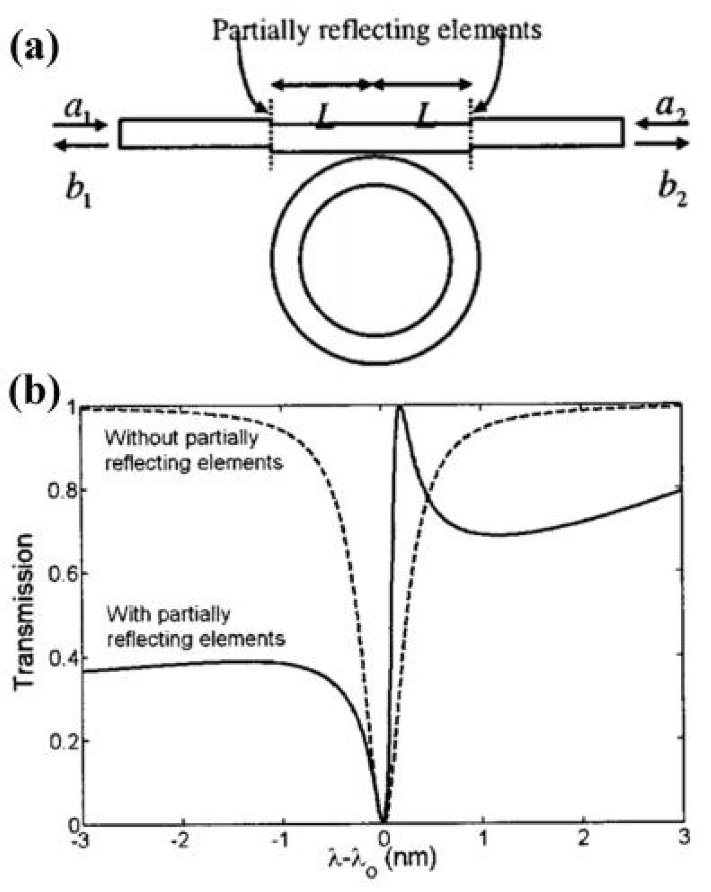
  113. On–Chip Biological and Chemical Sensing with Reversed Fano Lineshape Enabled by Embedded Microring Resonators. IEEE J. Sel. Top. Quantum Electron. 2013, 20, 35–44. [CrossRef]
  114. Wittstock, A.; Biener, J.; Bäumer, M. Chapter 1. Introduction to Nanoporous Gold; Lawrence Livermore National Lab. (LLNL): Livermore, CA, USA, 2012; pp. 1–10. [Google Scholar] [CrossRef]
  115. Lang, X.Y.; Guan, P.F.; Fujita, T.; Chen, M.W. Tailored nanoporous gold for ultrahigh fluorescence enhancement. Phys. Chem. Chem. Phys. 2011, 13, 3795–3799. [Google Scholar] [CrossRef]
  116. Lospinoso, D.; Colombelli, A.; Lomascolo, M.; Rella, R.; Manera, M.G. Self–Assembled Metal Nanohole Arrays with Tunable Plasmonic Properties for SERS Single–Molecule Detection. Nanomaterials 2022, 12, 380. [Google Scholar] [CrossRef] [PubMed]
  117. Oo, S.Z.; Silva, G.; Carpignano, F.; Noual, A.; Pechstedt, K.; Mateos, L.; Grant–Jacob, J.A.; Brocklesby, B.; Horak, P.; Charlton, M.; et al. A nanoporous gold membrane for sensing applications. Sens. Bio–Sens. Res. 2016, 7, 133–140. [Google Scholar] [CrossRef]
  118. Li, W.; Lv, S.; Wang, Y.; Zhang, L.; Cui, X. Nanoporous gold induced vertically standing 2D NiCo bimetal–organic framework nanosheets for non–enzymatic glucose biosensing. Sens. Actuators B Chem. 2018, 281, 652–658. [Google Scholar] [CrossRef]
  119. Zhao, F.; Zeng, J.; Arnob, M.P.; Sun, P.; Qi, J.; Motwani, P.; Gheewala, M.; Li, C.-H.; Paterson, A.; Strych, U.; et al. Monolithic NPG nanoparticles with large surface area, tunable plasmonics, and high–density internal hot–spots. Nanoscale 2014, 6, 8199–8207. [Google Scholar] [CrossRef] [PubMed]
  120. Ruffato, G.; Garoli, D.; Cattarin, S.; Barison, S.; Romanato, F. FIB lithography of nanoporous gold slits for extraordinary transmission. Microelectron. Eng. 2012, 98, 419–423. [Google Scholar] [CrossRef]
  121. Qi, J.; Motwani, P.; Gheewala, M.; Brennan, C.; Wolfe, J.C.; Shih, W.-C. Surface–enhanced Raman spectroscopy with monolithic nanoporous gold disk substrates. Nanoscale 2013, 5, 4105–4109. [Google Scholar] [CrossRef]
  122. Li, M.; Zhao, F.; Zeng, J.; Qi, J.; Lu, J.; Shih, W.-C. Microfluidic surface–enhanced Raman scattering sensor with monolithically integrated nanoporous gold disk arrays for rapid and label–free biomolecular detection. J. Biomed. Opt. 2014, 19, 111611. [Google Scholar] [CrossRef] [PubMed]
  123. Rao, W.; Wang, D.; Kups, T.; Baradács, E.; Parditka, B.; Erdélyi, Z.; Schaaf, P. Nanoporous Gold Nanoparticles and Au/Al2O3 Hybrid Nanoparticles with Large Tunability of Plasmonic Properties. ACS Appl. Mater. Interfaces 2017, 9, 6273–6281. [Google Scholar] [CrossRef] [PubMed]
  124. Qiu, S.; Zhao, F.; Zenasni, O.; Li, J.; Shih, W.-C. Nanoporous Gold Disks Functionalized with Stabilized G–Quadruplex Moieties for Sensing Small Molecules. ACS Appl. Mater. Interfaces 2016, 8, 29968–29976. [Google Scholar] [CrossRef] [PubMed]
  125. Qiu, S.; Zhao, F.; Zenasni, O.; Li, J.; Shih, W.-C. Catalytic assembly of DNA nanostructures on a nanoporous gold array as 3D architectures for label–free telomerase activity sensing. Nanoscale Horiz. 2017, 2, 217–224. [Google Scholar] [CrossRef] [PubMed]
  126. Ebbesen, T.W.; Lezec, H.J.; Ghaemi, H.F.; Thio, T.; Wolff, P.A. Extraordinary optical transmission through sub–wavelength hole arrays. Nature 1998, 391, 667–669. [Google Scholar] [CrossRef]
  127. Zhu, X.; Cao, N.; Thibeault, B.J.; Pinsky, B.; Yanik, A.A. Mechanisms of Fano–resonant biosensing: Mechanical loading of plasmonic oscillators. Opt. Commun. 2020, 469, 125780. [Google Scholar] [CrossRef]
  128. Yanik, A.A.; Cetin, A.E.; Huang, M.; Artar, A.; Mousavi, S.H.; Khanikaev, A.; Connor, J.H.; Shvets, G.; Altug, H. Seeing protein monolayers with naked eye through plasmonic Fano resonances. Proc. Natl. Acad. Sci. USA 2011, 108, 11784–11789. [Google Scholar] [CrossRef]
  129. Wang, Y.; Ao, S.; Yang, F.; Zhang, Z.; Zhao, Y. Coupling between Surface Plasmon Modes of Single–Layer Complex Silver Nanohole Arrays and Enhancing Index Sensing. ACS Appl. Nano Mater. 2022, 5, 9761–9770. [Google Scholar] [CrossRef]
  130. Singh, R.; Cao, W.; Al–Naib, I.; Cong, L.; Withayachumnankul, W.; Zhang, W. Ultrasensitive terahertz sensing with high–Q Fano resonances in metasurfaces. Appl. Phys. Lett. 2014, 105, 171101. [Google Scholar] [CrossRef]
  131. Ding, C.; Jiang, L.; Wu, L.; Gao, R.; Xu, D.; Zhang, G.; Yao, J. Dual–band ultrasensitive THz sensing utilizing high quality Fano and quadrupole resonances in metamaterials. Opt. Commun. 2015, 350, 103–107. [Google Scholar] [CrossRef]
  132. Gupta, M.; Srivastava, Y.K.; Manjappa, M.; Singh, R. Sensing with toroidal metamaterial. Appl. Phys. Lett. 2017, 110, 121108. [Google Scholar] [CrossRef]
  133. Tan, T.C.W.; Plum, E.; Singh, R. Lattice-Enhanced Fano Resonances from Bound States in the Continuum Metasurfaces. Adv. Opt. Mater. 2020, 8, 1901572. [Google Scholar] [CrossRef]
  134. Zhao, H.; Feng, L. Parity–time symmetric photonics. Natl. Sci. Rev. 2018, 5, 183–199. [Google Scholar] [CrossRef]
  135. Wiersig, J. Enhancing the Sensitivity of Frequency and Energy Splitting Detection by Using Exceptional Points: Application to Microcavity Sensors for Single–Particle Detection. Phys. Rev. Lett. 2014, 112, 203901. [Google Scholar] [CrossRef]
  136. Zhu, J.; Liu, H.; Bo, F.; Tao, C.; Zhang, G.; Xu, J. Intuitive model of exceptional points in an optical whispering–gallery microcavity perturbed by nanoparticles. Phy. Rev. A 2020, 101, 053842. [Google Scholar] [CrossRef]
  137. Hodaei, H.; Miri, M.-A.; Heinrich, M.; Christodoulides, D.N.; Khajavikhan, M. Parity–time–symmetric microring lasers. Science 2014, 346, 975–978. [Google Scholar] [CrossRef]
  138. Rüter, C.E.; Makris, K.G.; El–Ganainy, R.; Christodoulides, D.N.; Segev, M.; Kip, D. Observation of parity–time symmetry in optics. Nat. Phys. 2010, 6, 192–195. [Google Scholar] [CrossRef]
  139. Ramezanpour, S.; Bogdanov, A.; Alù, A.; Ra’Di, Y. Generalization of exceptional point conditions in perturbed coupled resonators. Phys. Rev. B 2021, 104, 205405. [Google Scholar] [CrossRef]
  140. Zhu, J.; Ozdemir, S.; Xiao, Y.-F.; Li, L.; He, L.; Chen, D.-R.; Yang, L. On–chip single nanoparticle detection and sizing by mode splitting in an ultrahigh–Q microresonator. Nat. Photonics 2009, 4, 46–49. [Google Scholar] [CrossRef]
  141. Hodaei, H.; Hassan, A.U.; Wittek, S.; Garcia–Gracia, H.; El–Ganainy, R.; Christodoulides, D.N.; Khajavikhan, M. Enhanced sensitivity at higher–order exceptional points. Nature 2017, 548, 187–191. [Google Scholar] [CrossRef]
  142. Li, X.-X.; Fang, Y.-T. Sensing gas through coupling effect of quasi–PT–symmetry resonators. J. Instrum. 2019, 14, P02010. [Google Scholar] [CrossRef]
  143. De Carlo, M.; De Leonardis, F.; Passaro, V.M.N. Design Rules of a Microscale PT–Symmetric Optical Gyroscope Using Group IV Platform. J. Light. Technol. 2018, 36, 3261–3268. [Google Scholar] [CrossRef]
  144. 146Chen, P.-Y.; Jung, J. PT Symmetry and Singularity–Enhanced Sensing Based on Photoexcited Graphene Metasurfaces. Phys. Rev. Appl. 2016, 5, 064018. [Google Scholar] [CrossRef]
  145. Wiersig, J. Sensors operating at exceptional points: General theory. Phys. Rev. A 2016, 93, 033809. [Google Scholar] [CrossRef]
  146. Liu, X.; Wang, H.; Zhang, J.; Guo, J.; Wu, X. Enhancement of Sensitivity Near Exceptional Point by Constructing Nonreciprocal Fiber Cavity Assisted by Isolator and Erbium–Doped Fiber. IEEE Sens. J. 2021, 21, 18823–18828. [Google Scholar] [CrossRef]
  147. Park, J.-H.; Ndao, A.; Cai, W.; Hsu, L.; Kodigala, A.; Lepetit, T.; Lo, Y.-H.; Kanté, B. Symmetry–breaking–induced plasmonic exceptional points and nanoscale sensing. Nat. Phys. 2020, 16, 462–468. [Google Scholar] [CrossRef]
  148. Zhong, Q.; Ren, J.; Khajavikhan, M.; Christodoulides, D.N.; Özdemir, K.; El–Ganainy, R. Sensing with Exceptional Surfaces in Order to Combine Sensitivity with Robustness. Phys. Rev. Lett. 2019, 122, 153902. [Google Scholar] [CrossRef]
  149. Zhang, X.; Ding, K.; Zhou, X.; Xu, J.; Jin, D. Experimental Observation of an Exceptional Surface in Synthetic Dimensions with Magnon Polaritons. Phys. Rev. Lett. 2019, 123, 237202. [Google Scholar] [CrossRef]
  150. Zhong, Q.; Hashemi, A.; Özdemir, K.; El–Ganainy, R. Control of spontaneous emission dynamics in microcavities with chiral exceptional surfaces. Phys. Rev. Res. 2021, 3, 013220. [Google Scholar] [CrossRef]
  151. Qin, G.; Xie, R.; Zhang, H.; Hu, Y.; Wang, M.; Li, G.; Xu, H.; Lei, F.; Ruan, D.; Long, G. Experimental Realization of Sensitivity Enhancement and Suppression with Exceptional Surfaces. Laser Photonics Rev. 2021, 15, 2000569. [Google Scholar] [CrossRef]
  152. Wang, Q.; Ding, K.; Liu, H.; Zhu, S.; Chan, C.T. Exceptional cones in 4D parameter space. Opt. Express 2020, 28, 1758–1770. [Google Scholar] [CrossRef]
  153. Yang, H.; Mao, X.; Qin, G.-Q.; Wang, M.; Zhang, H.; Ruan, D.; Long, G.-L. Scalable higher–order exceptional surface with passive resonators. Opt. Lett. 2021, 46, 4025. [Google Scholar] [CrossRef] [PubMed]
  154. Bender, C.M.; Boettcher, S. Real Spectra in Non–Hermitian Hamiltonians HavingPTSymmetry. Phys. Rev. Lett. 1998, 80, 5243–5246. [Google Scholar] [CrossRef]
  155. Özdemir, K.; Rotter, S.; Nori, F.; Yang, L. Parity–time symmetry and exceptional points in photonics. Nat. Mater. 2019, 18, 783–798. [Google Scholar] [CrossRef] [PubMed]
  156. Liu, Q.; Wang, B.; Ke, S.; Long, H.; Wang, K.; Lu, P. Exceptional points in Fano–resonant graphene metamaterials. Opt. Express 2017, 25, 7203–7212. [Google Scholar] [CrossRef]
  157. Liu, Z.-P.; Zhang, J.; Özdemir, K.; Peng, B.; Jing, H.; Lü, X.-Y.; Li, C.-W.; Yang, L.; Nori, F.; Liu, Y.-X. Metrology with PT–Symmetric Cavities: Enhanced Sensitivity near the PT–Phase Transition. Phys. Rev. Lett. 2016, 117, 110802. [Google Scholar] [CrossRef]
  158. Sakhdari, M.; Farhat, M.; Chen, P.-Y. PT–symmetric metasurfaces: Wave manipulation and sensing using singular points. New J. Phys. 2017, 19, 065002. [Google Scholar] [CrossRef]
  159. Zhao, D.; Ke, S.; Liu, Q.; Wang, B.; Lu, P. Giant Goos–Hänchen shifts in non–Hermitian dielectric multilayers incorporated with graphene. Opt. Express 2018, 26, 2817–2828. [Google Scholar] [CrossRef]
  160. Ren, J.; Hodaei, H.; Harari, G.; Hassan, A.U.; Chow, W.; Soltani, M.; Christodoulides, D.; Khajavikhan, M. Ultrasensitive micro–scale parity–time–symmetric ring laser gyroscope. Opt. Lett. 2017, 42, 1556–1559. [Google Scholar] [CrossRef]
  161. Jouybari, S.N. Refractive index measurement using coupled micro–resonator laser based on parity–time symmetry breaking. J. Mod. Opt. 2015, 63, 798–803. [Google Scholar] [CrossRef]
  162. Cong, L.; Manjappa, M.; Xu, N.; Al–Naib, I.; Zhang, W.; Singh, R. Fano Resonances in Terahertz Metasurfaces: A Figure of Merit Optimization. Adv. Opt. Mater. 2015, 3, 1537–1543. [Google Scholar] [CrossRef]
  163. Özdemir, K.; Zhu, J.; He, L.; Yang, L. Estimation of Purcell factor from mode–splitting spectra in an optical microcavity. Phys. Rev. A 2011, 83, 033817. [Google Scholar] [CrossRef] [Green Version]
Figure 1. (a) Fano profile with different q values. Adapted with permission from Ref. [21]. Copyright (2010), American Physical Society. (b) The scattering cross–section of Fano with different b values. Adapted with permission from Ref. [54]. Copyright (2011), American Physical Society.
Chemosensors 10 00397 g001
Figure 2. (a) The schematic diagram for the nanoshell heptamer. Adapted with permission from Ref. [65]. (b) The hybrid bonding mode. (c) The hybrid anti–bonding mode.
Chemosensors 10 00397 g002
Figure 3. (a) Schematic and geometrical parameters of a tilted metallic nano–groove antenna array. Adapted with permission from Ref. [70]. Copyright (2021), Optical Society of America. (b) Linewidth Fano resonance versus φ.
Chemosensors 10 00397 g003
Figure 4. (a) Diagram of asymmetric resonant ring with analyte. Adapted with permission from Ref. [73]. Copyright (2014), AIP Publishing LLC. (b) The transmission of Fano resonance with different analytes.
Chemosensors 10 00397 g004
Figure 5. (a) Schematic diagram of the two double–layer graphene–based plasmonic structures. Adapted with permission from Ref. [91]. Copyright (2018), the authors. (b) The transmission spectra of this terahertz graphene–layered metamaterial structure. (c) The detailed diagram of the active Fano resonance structure. Adapted with permission from Ref. [95]. Copyright (2019), Wiley–VCH Verlag GmbH & Co. KGaA, Weinheim. (d) The measured transmission coefficients S21 of the passive and active Fano resonance structures.
Chemosensors 10 00397 g005
Figure 6. (a) Schematic of metal–dielectric multilayer Kretschmann configuration under TM–polarized light. Adapted with permission from Ref. [96]. (b) Schematic configuration depicts the geometrical parameters of capped nanoslits. Adapted with permission from Ref. [100]. (c) 2D schematic describing the critical parameters of the sensor. Adapted with permission from Ref. [109]. Copyright (2022), Elsevier Ltd. (d) The transmission spectrum obtained when opening size (d1).
Chemosensors 10 00397 g006
Figure 7. (a) A microring resonator with two partially reflecting elements. Adapted with permission from Ref. [111]. Copyright (2003), American Institute of Physics. (b) Symmetric resonance spectrum of a conventional microring resonator and asymmetric Fano resonance of one with reflecting elements.
Chemosensors 10 00397 g007
Figure 8. (a) Schematic diagram of the experimental setup for biomolecular detection based on Fano resonance. Adapted with permission from Ref. [127]. Copyright (2020), 2020 Elsevier B.V. (b) Experimentally measured transmission spectra with different tested materials on the NHAs. (c) Sensitivities of the Fano EOT transmission dip and peak.
Chemosensors 10 00397 g008
Figure 9. (a) The WGM resonator. Adapted with permission from Ref. [137]. Copyright (2016), American Physical Society. (b) Two–coupled WGM resonator. Adapted with permission from Ref. [141]. Copyright (2018), Chinese Laser Press. (c) Schematic of a bilayer periodic plasmonic structure composed of two optically dissimilar plasmonic resonator arrays with detuned resonances. Adapted with permission from Ref. [147]. (d) Schematic of nanoscale sensing of the environmental RI variation within the box region surrounding the GNR. Adapted with permission from Ref. [50]. Copyright (2022), Chinese Laser Press. (e) Absolute value variation in the eigenvalue difference between the hybrid modes of the plasmon–exciton sensor in response to environmental RI change.
Chemosensors 10 00397 g009
Figure 10. (a) The concept map of ES. Adapted with permission from Ref. [148]. Copyright (2019), American Physical Society. (b) Schematic diagram of the ES photonic structure. (c) Diagram of unidirectional coupling ES structure. Adapted with permission from Ref. [151]. Copyright (2021), Wiley−VCH GmbH. (d) Diagram of magnon polariton system. Adapted with permission from Ref. [149]. Copyright (2019), American Physical Society. (e) Slices of ES in the 3D parameter space (x, y, θ).
Chemosensors 10 00397 g010
Figure 11. (a) The change process of real part of eigenvalue of the system. Adapted with permission from Ref. [155]. (b) The change process of imaginary part of eigenvalue of the system.
Chemosensors 10 00397 g011
Figure 12. (a) Schematic integration of a PT–symmetric system. Adapted with permission from Ref. [144]. Copyright (2016), American Physical Society. (b) Frequency of the rB dip and the value of the exceptional point (bottom) as a function of the dopant concentration for the graphene–based PT–symmetric sensor. (c) Non−Hermitian multilayer media structure based on GH displacement, where A and B are the primitive unit–cell layer, C presents graphene layer and D is dielectric layer. Adapted with permission from Ref. [159]. Copyright (2018), Optical Society of America. (d) Correlation between sensitivity coefficient and real part of D–layer RI.
Chemosensors 10 00397 g012
Figure 13. (a). Resonance strength of Fano versus structural asymmetry parameter. Adapted with permission from Ref. [162]. Copyright (2017), American Chemical Society. (b) Q factor of Fano resonance versus structural asymmetry parameter. (c) Effect on the splitting quality factor Qsp. Adapted with permission from Ref. [46].
Chemosensors 10 00397 g013
Table 1. Examples of Fano resonance biosensors.
StructureAnalyteSensitivityQFOMYearRef.
Split ring–perfect ringDielectric material1225 nm/RIU30.42015[64]
Antisymmetric eight–member nanoshell oligomerMixed liquids22.52015[67]
Metal nano–groove arrayNaCl solution657 nm/RIU2632021[70]
L–nanoarrayDielectric material1360 nm/RIU292018[71]
Double two–split nanoringsHealthy and cancerous tissues594 nm/RIU5663782019[72]
Asymmetrical split–resonance rings394.5371.92015[88]
Active split–ring resonators based on grapheneAnalyte coated1.87021 THz/RIU2016[90]
Multilayer grapheneAnalyte coated7885 nm/RIU97862018[91]
Metal grating arrayBSA and anti–BSA460 nm/RIU582019[100]
MIMGlucose solution1300 nm/RIU39.3829.552022[109]
Load the partially reflected microloopGlucose solution0.024% or 24 n g/dL2003[111]
Waveguide coupled with a microring resonatorK+ ions density of KxMoO3154.3 nm/RIU2021[112]
Embedded–ring resonatorsMixed liquids1.21 × 104 nm/RIU2014[113]
Splitting ring arrayAnalyte coated7.75 × 103 nm/RIU282014[123]
Plasmonic nanohole arrayMonolayer of protein~53 nm/RIU2020[127]
Nanohole arrayNaCl solutions690.12 nm/RIU2001622011[128]
Nanorods in nanopore arrays1200.6 nm/RIU279.22022[129]
Broken ring arrayAnalyte coated2.06 × 104 nm/RIU382015[131]
Asymmetric split–ring resonatorAnalyte coated7.32 × 104 nm/RIU9.62017[132]
Table 2. Examples of EP biosensors.
StructureAnalyteSensitivityYearRef.
Optical tunneling effect resonatorCarcinoembryonic antigen17,120 nm/IP2022[49]
Plasmon–exciton system RI of gold nanorod100 THz/RIU2022[50]
Active graphene metasurfaceDensity of charged impurities1.15 GHz/um22016[142]
Bilayer periodic plasmonic structureRI coating 671 nm/RIU2020[147]
Optical gyroscopeAngular velocity0.1–100°/h2017[160]
PT–symmetrically coupled microdisk RI of cavity 83 nm/RIU2015[161]
Publisher’s Note: MDPI stays neutral with regard to jurisdictional claims in published maps and institutional affiliations.

