Article

A New Approach for Approximate Solution of ADE: Physical-Based Modeling of Carriers in Doping Region

by
Leobardo Hernandez-Gonzalez
1,*,
Jazmin Ramirez-Hernandez
1,
Oswaldo Ulises Juarez-Sandoval
1,
Miguel Angel Olivares-Robles
1,
Ramon Blanco Sanchez
2 and
Rosario del Pilar Gibert Delgado
1
1
Instituto Politecnico Nacional, Escuela Superior de Ingenieria Mecanica y Electrica, Unidad Culhuacan, Av. Santa Ana No. 1000, Col. San Francisco Culhuacan, Mexico City C.P. 04430, Mexico
2
Departamento de Matemática, Universidad de Camaguey Ignacio Agramonte Loynaz, Camagüey C.P. 70100, Cuba
*
Author to whom correspondence should be addressed.
Mathematics 2021, 9(5), 458; https://doi.org/10.3390/math9050458
Submission received: 10 February 2021 / Revised: 20 February 2021 / Accepted: 22 February 2021 / Published: 24 February 2021
(This article belongs to the Section Engineering Mathematics)

Abstract

:
The electric behavior in semiconductor devices is the result of the electric carriers’ injection and evacuation in the low doping region, N-. The carrier’s dynamic is determined by the ambipolar diffusion equation (ADE), which involves the main physical phenomena in the low doping region. The ADE does not have a direct analytic solution since it is a spatio-temporal second-order differential equation. The numerical solution is the most used, but is inadequate to be integrated into commercial electric circuit simulators. In this paper, an empiric approximation is proposed as the solution of the ADE. The proposed solution was validated using the final equations that were implemented in a simulator; the results were compared with the experimental results in each phase, obtaining a similarity in the current waveforms. Finally, an advantage of the proposed methodology is that the final expressions obtained can be easily implemented in commercial simulators.

1. Introduction

In recent years, several investigations have been carried out in the field of power device modeling with the aim of obtaining electrical simulations closer to their experimental measurements. The main problem that arises in obtaining a practical model is the proper description of the behavior of the chargers’ distribution in the N-region. To obtain the loads’ behavior model, the electron and hole currents that are injected during the switching phases need to be calculated.
The electric behavior in semiconductor devices is the result of the electrical chargers’ injection and evacuation in the low doping region, N-. The carrier dynamics is determined by the ambipolar diffusion equation (ADE) solution, where the expression involves the main physical phenomena in the low doping region.
In the literature, some ADE solution methodologies have been reported. However, an analytic solution cannot be obtained because it is a second-order differential equation that depends on time and distance [1,2]. The ADE solutions reported in the literature are classified into two methodologies: numerical solution and approximate solution. The numerical solution gives more exactitude; however, it is not suitable for electrical simulators in contrast with the approximate solution.
The approximate solution is suitable for designers of electrical circuits and can be mainly subdivided into the separation of variables, transformation techniques (Laplace, Fourier), and concentrated electrical chargers [3,4,5,6,7,8,9,10,11,12,13,14,15]; this last type of methodology is one of the most practical, efficient, and focuses mainly on the calculation and modeling of the carriers’ concentration in the N-region that allows the adequate description of the static and dynamic behavior of the semiconductor power devices.
In the literature, limited ADE solution methods based on the N-region modeling are presented. In [6,7,8,9,10,11,12,13,14,15,16,17], it is considered a discretization of the N-region, which includes the movement of the borders in space (xl and xr). In this solution, the authors used the Newton–Raphson method. However, it requires a pre-process of two to four iterations per simulation step; therefore, this solution is not suitable for implementation in electrical circuit simulators.
In [18,19], the use of a three-phase approximation for the turned-off condition was proposed. In each phase, a linearization of the gradient of the charges that occurred in the N-region was obtained; however, the models’ high complexity limited its implementation only to the SABER simulator.
In [20], the N-region was divided into five to ten subregions, where the concentration of carriers was approximated through a second-order polynomial equation with coefficients that varied in time. Due to its complexity, this solution is not suitable for implementation in a commercial electrical simulator.
In [21], to describe the dynamic behavior, the Rayleigh–Ritz method was used in combination with an approximation of the normalized position variable. In this, the final expressions obtained were in a function of time and were easy to solve; however, its implementation was limited only to the SABER simulator.
In [22,23], the ADE solution was presented using the finite element method, obtaining an electrical equivalent for an analogic solution; however, due to the use of the finite element method, its use in electrical circuit simulators becomes impractical.
In [24,25], a Fourier series-based ADE solution was obtained, where the methodology converted the ADE into a finite arrangement of first-order differential equations with variable Fourier coefficients. The accuracy of the model depends on the number of terms used. Therefore, its implementation in electrical circuit simulators is impractical.
In [26], the principle of physical modeling of a power diode was presented based in an approximate solution, however, only a two-dimensional variable analysis was presented.
In this paper, an empirical approximation of the ADE solution is proposed, presenting a detailed procedure and a three-dimensional variable analysis of the carriers’ behavior. It allows the simulation of the main physical phenomena associated with the low doping region in bipolar semiconductor devices, obtaining the carriers’ injection and evacuation of the N-region. The proposed solution solves the ADE as a function on the ambipolar diffusion length adjustment (L), which is achieved by using a simplified semi-theoretical approach. Some of the advantages of this modeling approach are listed below:
  • Facility of implementation in circuit simulators through analog electrical components with the system of equations developed as a solution of the ADE.
  • The mathematical procedure to solve the spatio-temporal second-order differential ADE equation is not complex in comparison to the numerical solutions proposed in the previous reported references.
  • The calculation variables used in each expression are a function of time and space, ensuring an adequate approximation with experimental values.
  • The developed model calculates the low doping zone width during the space charge accumulation, allowing the excess of the carriers’ injected calculation on the N-region.
  • A three-dimensional variable analysis of the carriers’ behavior is presented.
  • The results show that the proposed solution is robust for its integration in commercial electrical circuit simulators.
  • The obtained solution ensures a balance between mathematical calculations and accuracy results that are appropriate for its use by electronic designers.
  • A graphical and numerical estimated error is presented to validate the accuracy of the obtained results.
The rest of this paper is organized as follows. In Section 2, the development to obtain the ADE is presented. The proposed empirical solution is described in Section 3. In Section 4, the simulation results that validate the proposed solution methodology are presented, and finally, the conclusions of the developed work are presented in Section 5.

2. Ambipolar Diffusion Equation (ADE)

The diode was one of the first semiconductor devices developed for applications in power circuits. This type of device has two junctions (P+N- and N-N+) with a high doping profile and an intermediate region (N-) with a low doping profile. In this type of power device, the N-region is injected with carriers during the conduction phase, reducing this region’s resistance during current flow. However, the injection of a high concentration of minority carriers within the N-region causes two main problems during switching conditions: overvoltage during the change from its OFF state to ON state and reverse recovery during the change from its ON state to OFF state [1,2]. Therefore, the correct solution proposal of the ADE for its implementation in commercial simulators is essential.
The behavior of the N-region of a diode can be simplified as shown in Figure 1, where an injection of carriers takes place in the N-region through two injectors: anode and cathode. The net flow of electrons and holes (carriers) in the semiconductor devices generates the currents Ip(0,t), In(0,t), Ip(WB,t), and In(WB,t).

2.1. Carrier Transport

The process in which the charge carriers, p(x,t) ≈ n(x,t) move is known as the carrier transport. The transport of the carrier is made through two basic mechanisms: drift and diffusion.

2.1.1. Drift Mechanisms

When an electric field, E (V/cm), is applied to the N-region, a drift movement in the direction of the electric field for holes (Vp) (opposite direction for electrons (Vn)) predominates over the disordered movement of the carriers by thermal agitation.
The drift movement is due to the carriers’ acceleration caused by the electric field. For small values of the electric field, the drift velocity is proportional to the applied electric field. The constant proportionality between the drift velocity and the electric field is called mobility, μn for electrons, and μp for holes [1,2].
The drift movement causes electrons and hole currents that are given by:
I n _ d r i f t = q A n V n = q A n μ n E ( a m p s )
I p _ d r i f t = q A p V p = q A p μ p E ( a m p s )
where A is the area of the N-region; n and p are the carriers; and Vn and Vp represent the average velocities of electrons and holes, respectively. The total drift current is the sum of electrons and hole currents caused by the electric field [1,2], which is given by,
I T _ d r i f t = q A ( n μ n + μ p p ) E [ A ]

2.1.2. Diffusion

When the carriers are not uniformly distributed in the semiconductor, there is a high concentration region movement to those of low concentration; it predominates over the carriers’ chaotic motion due to thermal agitation. The diffusion of an electron (or hole) from a high concentration region to a low concentration produces a flow of electrons (or holes). The electron and hole currents are proportional to their concentration gradients, which are expressed, in one dimension [1,2], as:
I n _ d i f u s i o n = q A D n d n d x
I p _ d i f u s i o n = q A D p d p d x
where Dn and Dp (cm2/s) are the diffusion coefficients for electrons and holes, respectively. The total diffusion current is the contribution of electrons and hole currents,
I T _ d i f f = q A D n d n d x q A D p d p d x
There is a high injection of carriers in semiconductor power devices, where np in the N-region, being dn/dxdp/dx. Equations (3) and (6) for the high injection condition are:
I n ( x ) b 1 + b I T + q A D d p d x
I p ( x ) 1 1 + b I T q A D d p d x
where D = 2 D n D p D n + D p .
D is the ambipolar diffusion coefficient. Equations (7) and (8) are known as transport equations, which allow for calculating the current of electrons and holes for any x value along the N-region under high injection conditions.

2.2. Carrier Control Model

When the carrier concentration is disturbed from its equilibrium value (n(x = 0), p(x = 0)), electrons and holes will try to return to equilibrium. In the injection of excess carriers, the return to equilibrium occurs through the process of recombination of the minority carriers injected with the majority carriers. In the case of the extraction of carriers, they will return to equilibrium through the electron-hole pair generation process. The time required to re-establish the equilibrium is known as the lifetime τ. The analytical expression that allows for calculating the current contribution due to changes in carrier concentration is the continuity equation for electrons and holes given by [1,2],
d n ( x , t ) d t 1 q A d I n d x + G n R n
d p ( x , t ) d t 1 q A d I p d x + G p R p
where Gn and Gp are the electrons and holes generation velocities, respectively. Rn and Rp are the recombination velocity of electron and hole, respectively.
The recombination velocities for electrons and holes, considering only the Shockley–Read–Hall recombination, SRH, and Δn ≈ Δp >> ni, are given by [1,2],
R p = p ( x , t ) τ p   and   R n = n ( x , t ) τ n
Equations (9) and (10) are rewritten, using Equation (11),
d n ( x , t ) d t = 1 q A d I n d x n ( x , t ) τ n
d p ( x , t ) d t = 1 q A d I p d x p ( x , t ) τ p
To obtain the carriers’ control, the equation is considered only p. If Equation (12) is integrated between the limits x = 0 and x = WB, a new expression is obtained given by,
0 W B I p x d x = q A 0 W B p ( x , t ) τ p d x q A 0 W B p ( x , t ) t d x
As:
Q B = q A 0 W B p ( x , t ) d x = q A W B p ( x , t )
d Q B d t = q A 0 W B p ( x , t ) t d x
combining Equations (14)–(16), which uses the value of the incoming current and the outgoing current of the N-region as a function of time, the carriers’ control expression is,
I p ( 0 ,   t ) I p ( W B ,   t ) = Q τ p + d Q d t
The equation that describes the dynamic and static behavior of the carriers in the N-region is obtained, combining Equations (8) and (17).
2 p ( x , t ) x 2 = p ( x , t ) L 2 + 1 D p ( x , t ) t
where L = D τ is known as the ambipolar diffusion length. Equation (18) is known as the ADE.
The solution of Equation (18) allows obtaining the injection of currents and the resistance in the N-region, given, respectively, by,
I n ( x , t ) = b I T 1 + b + q A D p ( x , t ) x
I p ( x , t ) = I T 1 + b q A D p ( x , t ) x
R N = 0 W B d x q A ( μ n n + μ p p ) = W B q A ( μ n n + μ p p )
With n N D ,   p p ( x , t )   a n d   Q 0 = q A N D W B μ n
R N = W B q A N D μ n + q A ( μ n + μ p ) p ( x , t ) = W B 2 q A N D W B μ n + q A W B p ( x , t ) ( μ n + μ p ) = W B 2 Q 0 μ n + Q B ( μ n + μ p )
where Q0 represents the stored carriers for thermodynamic equilibrium.

3. The Empirical Solution of the ADE

The N-regions’ behavior depends on two phases, known as static and dynamic phases.

3.1. Static Phase

Under the static conditions: p ( x , t ) t = 0 , the concentration of carriers will only depend on the variable x, hence Equation (18) can be expressed as:
d 2 p ( x ) d x 2 p ( x ) L S 2 = 0
On the other hand, considering the initial conditions of concentration P0 and PW at x = 0 and x = WB, the solution of Equation (23) is given by
p ( x ) = P W sinh ( x L S ) + P 0 sinh ( W B x L S ) sinh ( W B L S )
Using Equation (24), the concentration gradients in the diode unions are given by,
p ( x ) x | x = 0 = 1 L S P W P 0 cosh ( W B L S ) sinh ( W B L S )
p ( x ) x | x = W B = 1 L S P W cosh ( W B L S ) P 0 sinh ( W B L S )
According to Equations (25) and (26), the currents Ip(x) and In(WB) are
I p ( x = 0 ) = I T 1 + b q A D L S P W P 0 cosh ( W B L S ) sinh ( W B L S )
I n ( x = W B ) = b I T 1 + b + q A D L S P W cosh ( W B L S ) P 0 sinh ( W B L S )
The expression given by Equation (29) represents the solution of Equation (15) through p(x) = Δp(x), which is used to obtain the excess of carriers injected on the N-region by ∆p(x).
Q B S ( x ) = q A L S ( P 0 + P W ) [ cosh ( W B L S ) 1 ] sinh ( W B L S )
as t a n h ( x 2 ) = c o s h ( x ) 1 s i n ( x ) , then
Q B S ( x ) = q A L S ( P 0 + P W ) tanh ( W B 2 L S )
The QBS(x) given by Equation (30) allows a better approximation of the carriers’ dynamic in the N-region. As QBS(x) is known, RN- is given by Equation (22).

3.2. Conduction Phase

This phase is divided into two states: activation and reverse blocking.

3.2.1. Activation

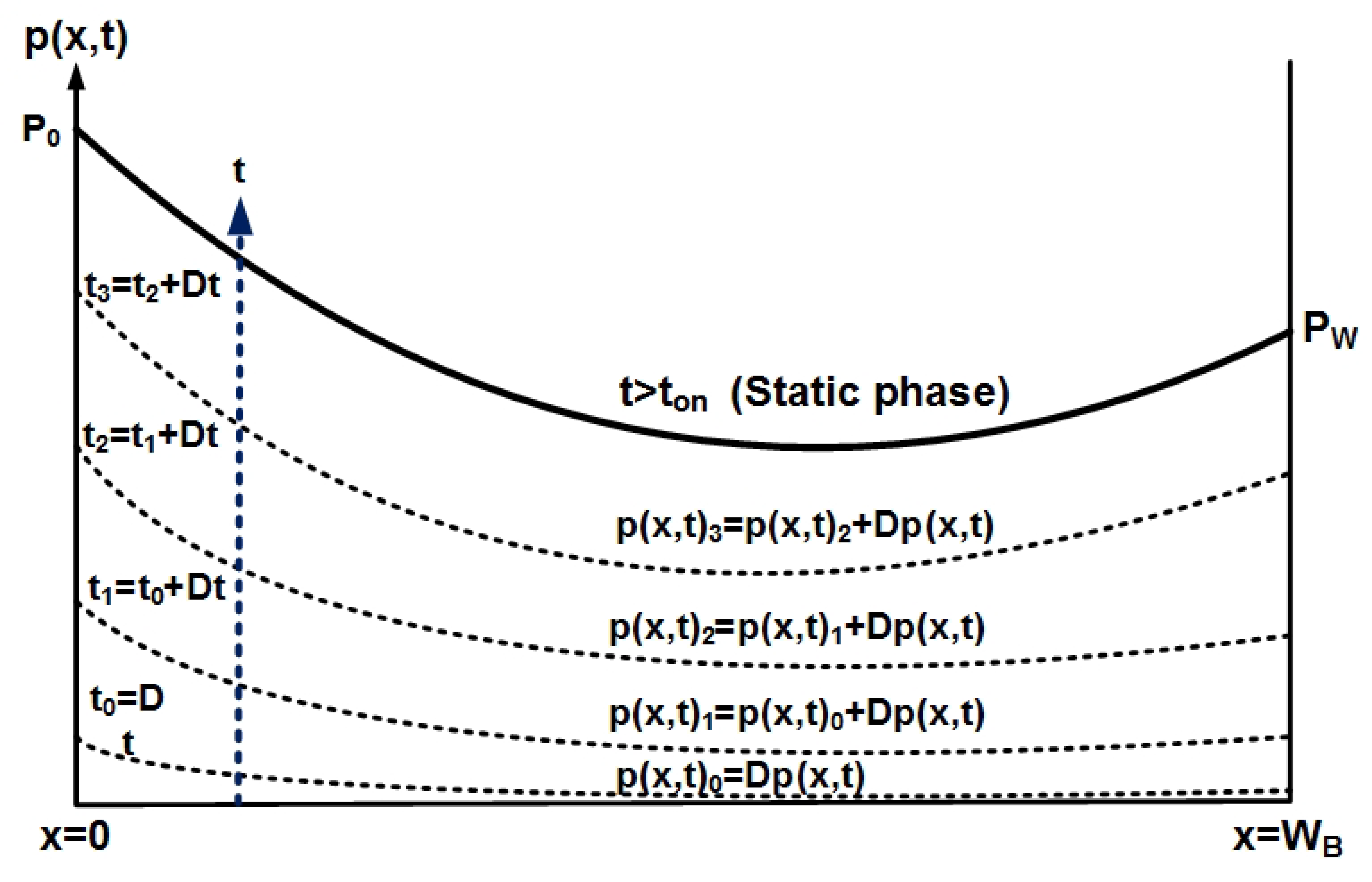
Figure 2 shows a typical carrier’s behavior during the activation phase, each time increment Δt is related with a non-linear increment in the concentration Δp(x,t); when the carriers’ increment is equal to zero, the activation phase ends. In this condition, any variation of Δt does not affect the carriers’ behavior; the previously analyzed condition p ( x , t ) t 0 is achieved.
As a result of the previous analysis, the increment of chargers in the N-region has a non-linear relationship inversely proportional to the time increment. This condition is formulated by:
p ( x , t ) t p ( x , t ) f n ( t )
where fn(t) is the time-dependent function. The ADE approximate solution requires the appropriate definition of the fn(t) function.
The main contribution of this paper is an approximated solution of the ADE that can be implemented on electronic simulators; according to this approach, an empiric first-order approximation of function is included and given by
p ( x , t ) t p ( x , t ) f ( t )
therefore, the ADE is rewritten as
2 p ( x , t ) x 2 p ( x , t ) D τ ( 1 + τ f ( t ) ) p ( x , t ) L o n 2 ( x , t )
where a new diffusion length is given by:
L o n ( x , t ) = L S 1 + τ f ( t ) = L S 2 1 + τ t
To calculate the excess of carriers injected into the N-region during the activation phase, combining Equations (33) and (15) with p(x,t) = Δp, a new expression is obtained given by:
Q o n ( x , t ) = q A L o n ( t ) ( P 0 + P W ) tanh ( x 2 L o n ( t ) )
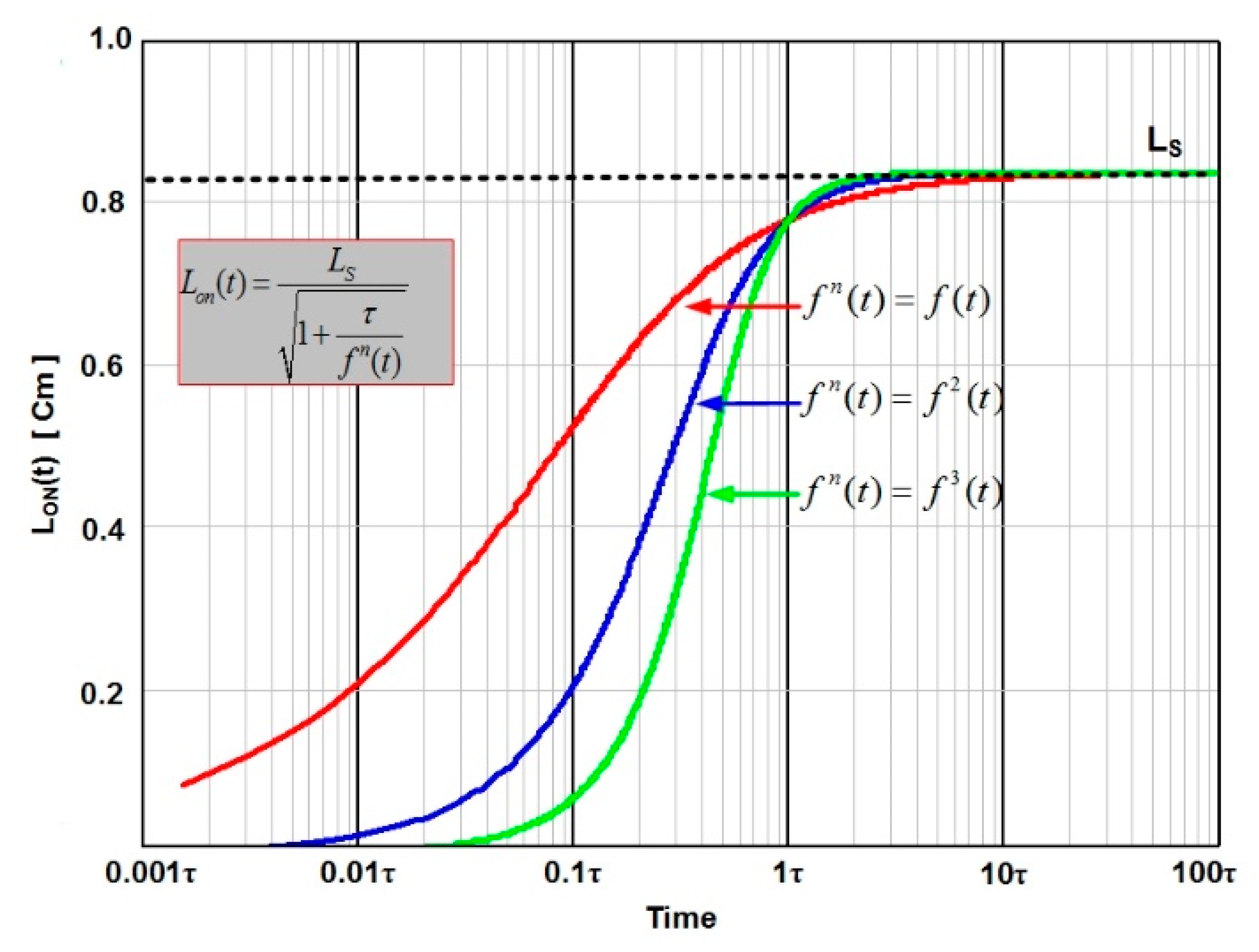
Figure 3 shows the Lon(t) response; this behavior considers a function approximation such as: fn(t) = f(t) and fn(t) = f2(t). In this way, the second-order approximation creates a fast evolution of Lon(t) to Ls that has a strong relation with the activation time.
At the beginning of the activation phase, p(x,t) has a strong time dependence through ambipolar diffusion length Lon(t). At the end of the activation phase, called the static phase, p(x,t) is independent of the time since Lon(t→∞) = Ls. As the expression in Equation (33) is similar to Equation (23), the solution of p(x,t) with L o n ( t ) is formulated by
p ( x , t ) = P W sinh ( x L o n ( t ) ) + P 0 sinh ( W B x L o n ( t ) ) sinh ( W B L o n ( t ) )
With Equation (36), the concentration gradients in the diode unions are obtained using the transportation equations in a similar way as Equations (25)–(28).

3.2.2. Blocking

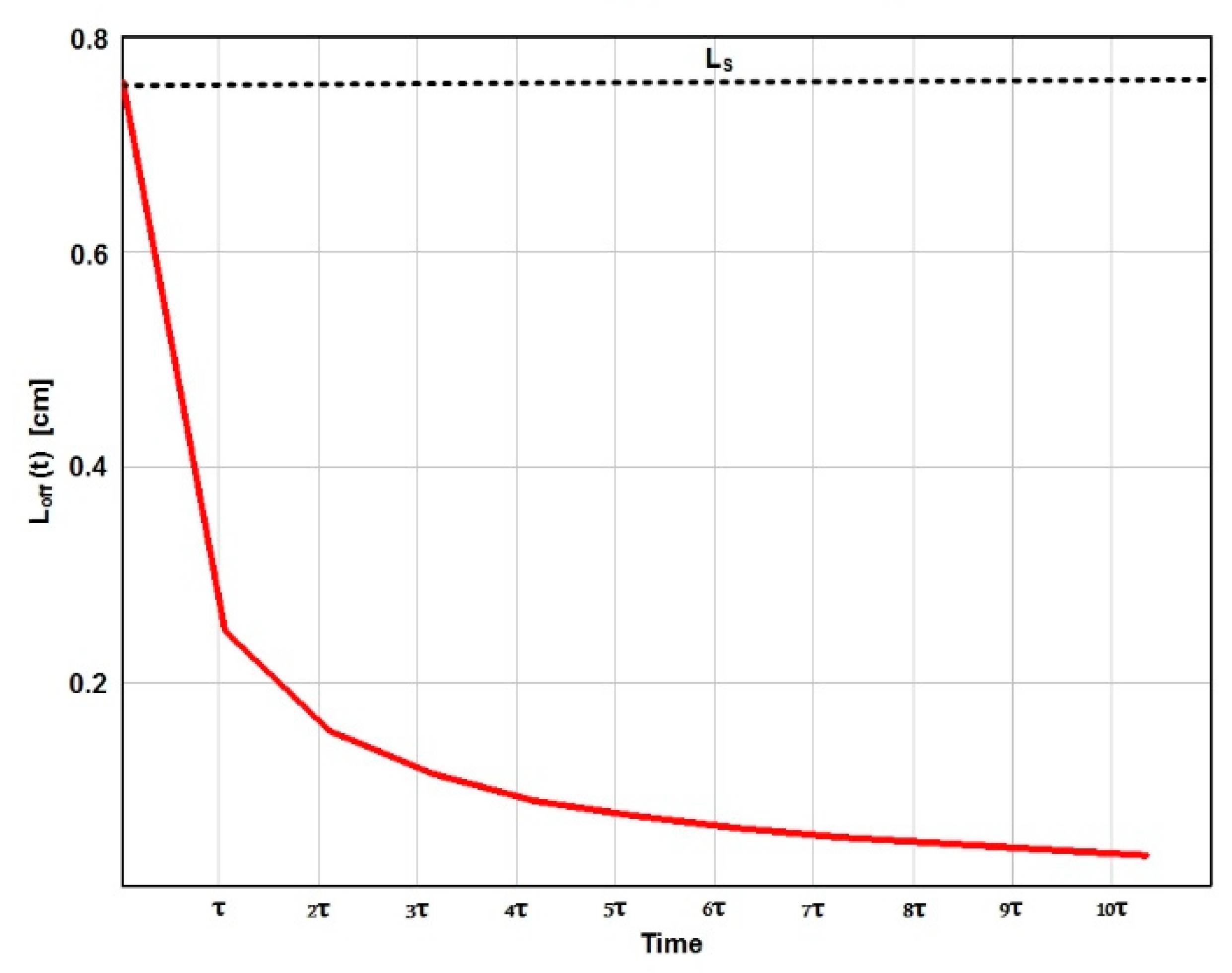
In this condition, the excess of carriers Δp(x,t) stored on the N-region during the activation phase are evacuated by both injectors. To model the blocking condition, a new diffusion length as a function of the time is proposed; notice that Loff, which begins in the Ls value, decreases to zero; to satisfy this condition, Loff is formulated by:
L o f f ( t ) = L S L S 2 1 + τ t
Figure 4 shows the Loff as a function of time. Note that according to the expected condition, Loff decreases from Ls to zero.
To quantify the carriers in the N-region during the inverse, the blocking phase was used Equation (38)
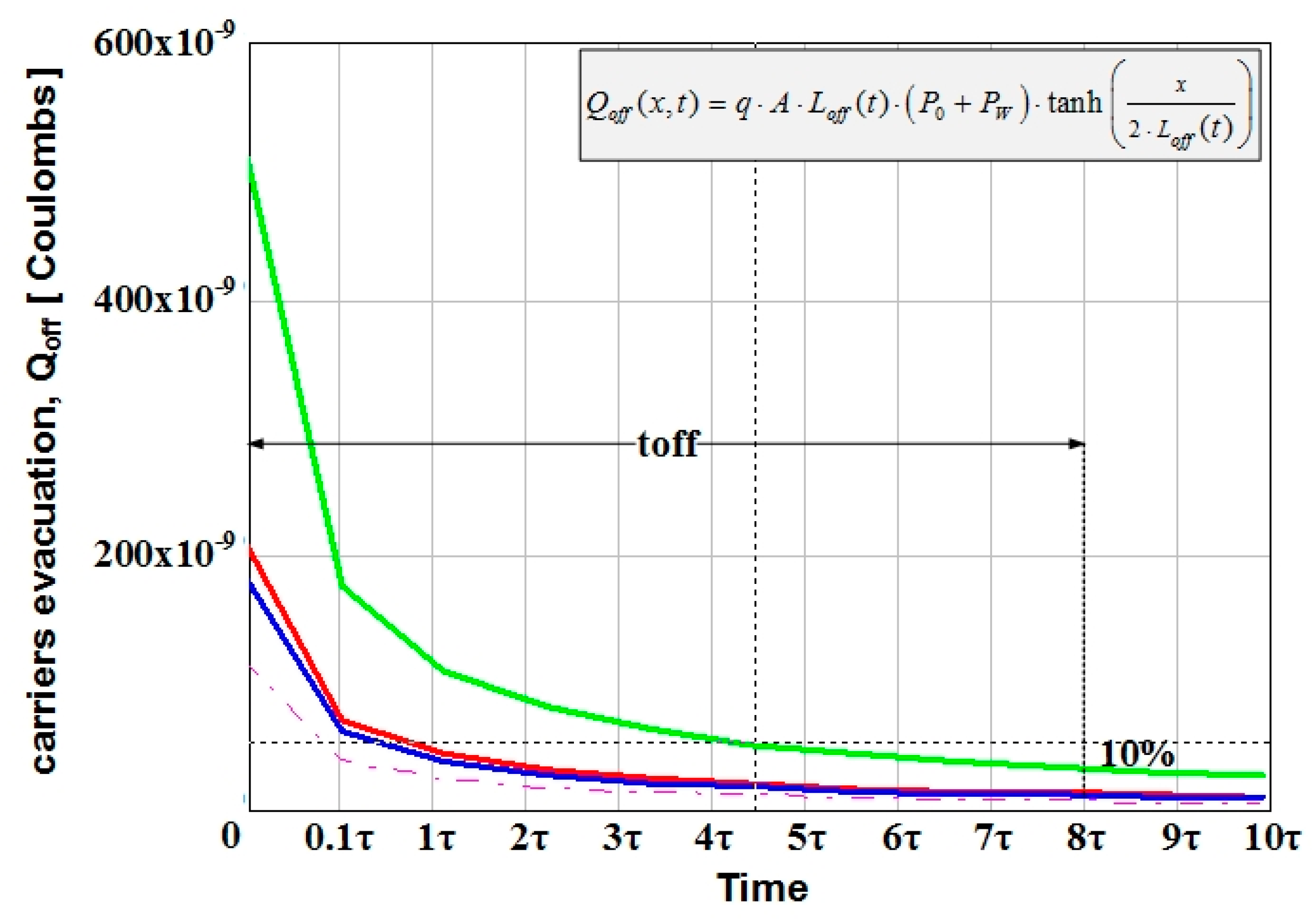
Q o f f ( x , t ) = q A L o f f ( t ) ( P 0 + P W ) tanh ( x 2 L o f f ( t ) )
Similar to the activation phase, p(x) as a function of Loff is given by Equation (39), which guarantees the evacuation of the N-region carriers.
p ( x , t ) = P W sinh ( x L o f f ( t ) ) + P 0 sinh ( W B x L o f f ( t ) ) sinh ( W B L o f f ( t ) )
with p(x,t) known, the concentration gradients in the diode unions are obtained to be used in the transportation equations in a similar way as Equations (25)–(28).

4. Simulation Results

In this section, the solution of ADE is given by Equations (24), (36) and (39), according to different phases: static, activation, and inverse blocking, and the data used were: A = 0.04 cm, W = 37 µm, τn = τp = 0.15 µs, µn = 947 cm2/Vs, µp = 108 cm2/Vs, and LS = 0.73. The simulation results showed that the adopted empirical approximation could obtain a feasible and reduced equation to model the injection and evacuation of carriers in the N-region and are easily implemented on commercial and non-commercial electronic simulators.

4.1. Static Phase

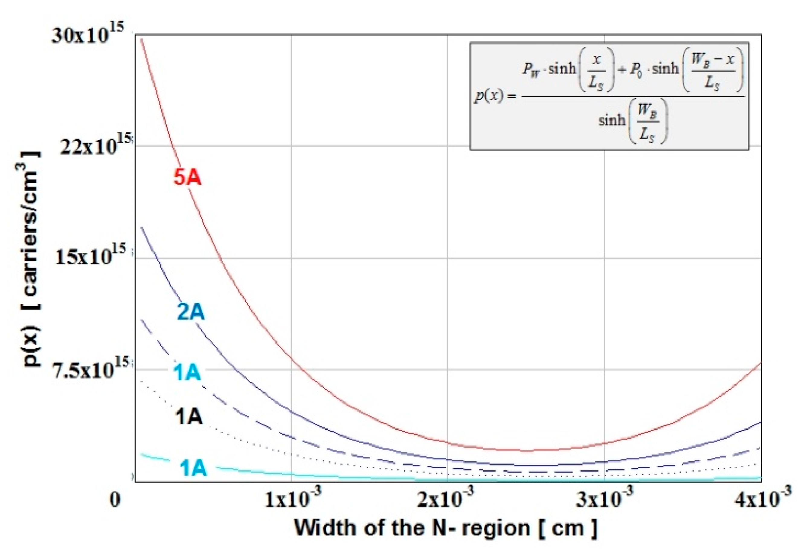
Figure 5 shows the p(x) response to different injected carrier values to the N-region. To obtain the density of charge, we used the expressions reported in [27]. Table 1 shows the total injected current to the N-region and the carriers’ concentration, P0, and PW.
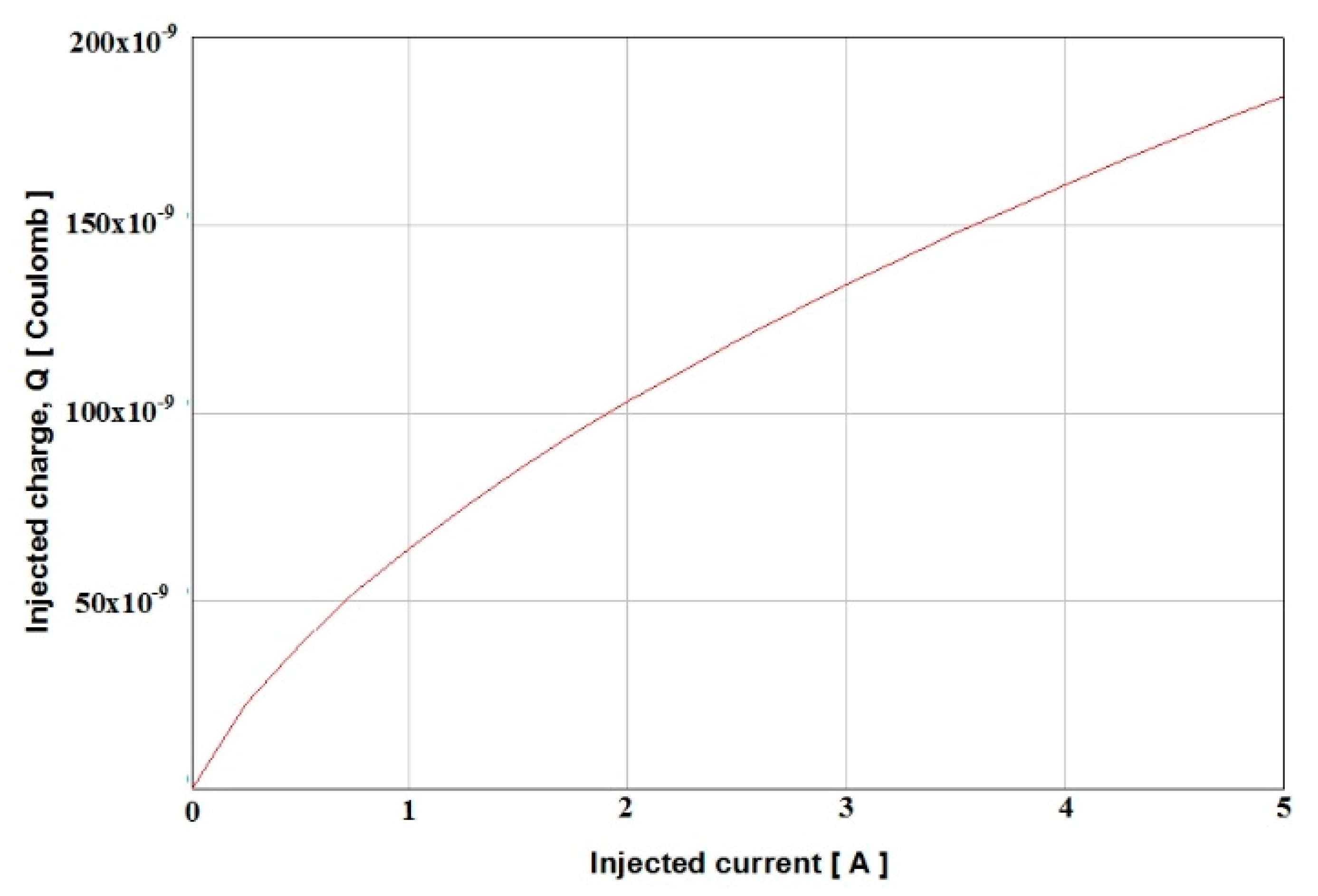
Figure 5 shows the density of carriers injected to the N-region, which increases according to the total injected current. Figure 6 shows the relation between the current and the carriers injected into the N-region.
Figure 7 shows the N-region resistance response according to the injected current, which decreases according to the injected currents with a proportional increment. This behavior of the resistance has a substantial impact on the analysis of conduction losses in power semiconductors.

4.2. Conduction Phase

The conduction phase begins when a current, different to zero, is injected in the N-region; in this phase, the carriers’ density in the N-region depends on the time the current changes from zero to a maximum value when the static phase begins.
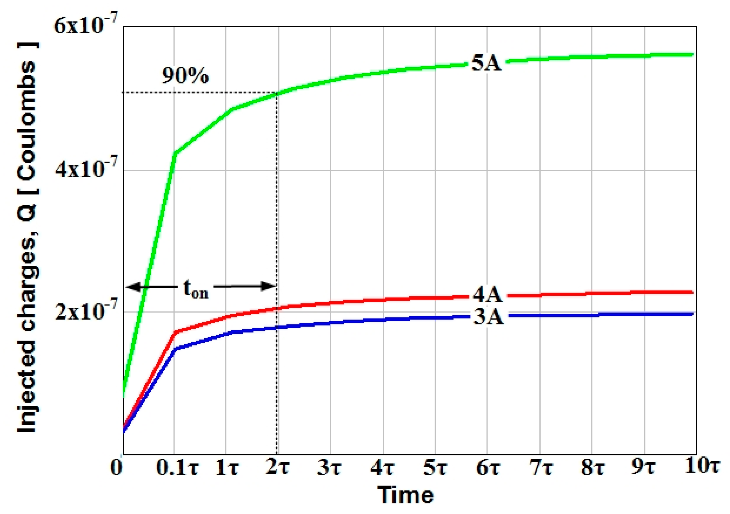
Figure 8 shows the injected carriers’ behavior for different maximum current values. At approximately t = 2τ, a value of 90% of IMAX = 5 A is reached; this being the activation time of the semiconductor device, ton, it can be verified that ton is dependent on the maximum current injected into the device.
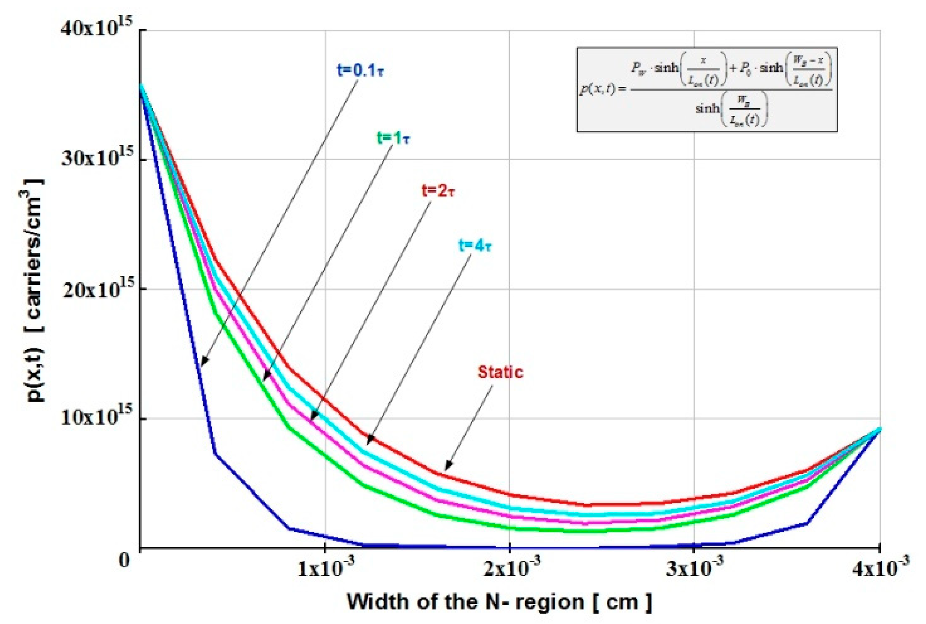
Figure 9 shows the p(x,t) evolution for a current injection in the range of 0 A to 5 A. When the carriers’ injection time increases, the static phase is reached. According to the Figure 9, it can be considered that at t = 4τ, the static phase begins since the increment of p(x,t) is small.
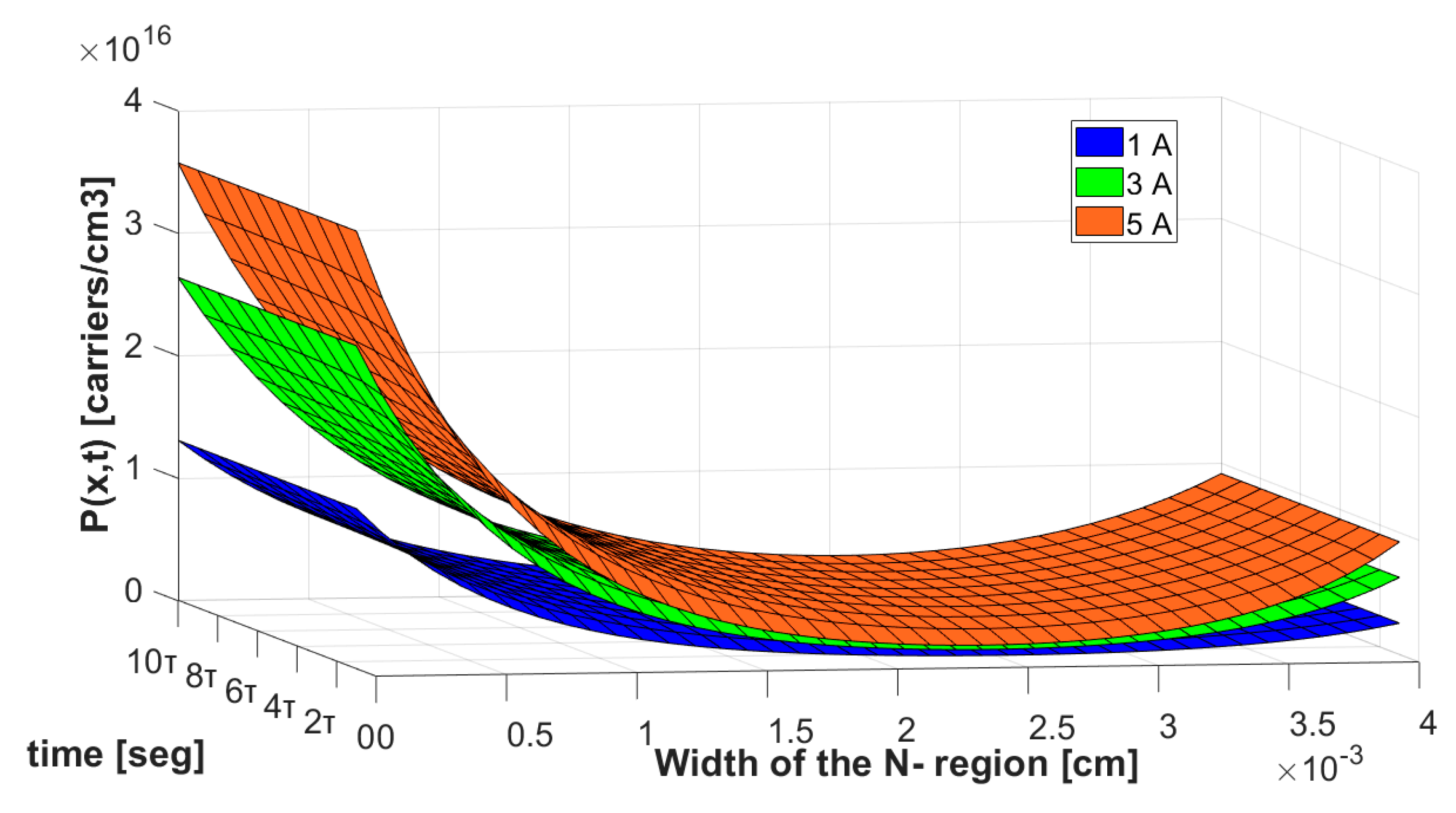
Figure 10 shows the evolution of p(x,t) for a time range from 2τ to 10τ for a maximum current injection of 1 A, 3 A, and 5 A.

4.3. Reverse Blocking Phase

The reverse blocking phase starts when the current in the N-region is reduced from a maximum (static) value to zero. In this phase, the carriers’ displacement is evaluated along the N-region. Figure 11 shows the carriers’ evacuation during the static phase from 5 A to 0 A.
At approximately t = 8τ, a value of 10% of IMAX = 5 A was reached, which indicates the deactivation time of the semiconductor device, toff. It can be verified that toff is dependent on the maximum static current that is evacuated in the device and which is always greater than ton.
Figure 12 shows the p(x,t) evolution for a current displacement from 5 A to 0 A; the evolution of p(x,t) from the static phase to zero was verified for different charge displacement times. For values of t greater than 10τ, it was considered that the reverse blocking had been reached since the decrements of p (x,t) were small.
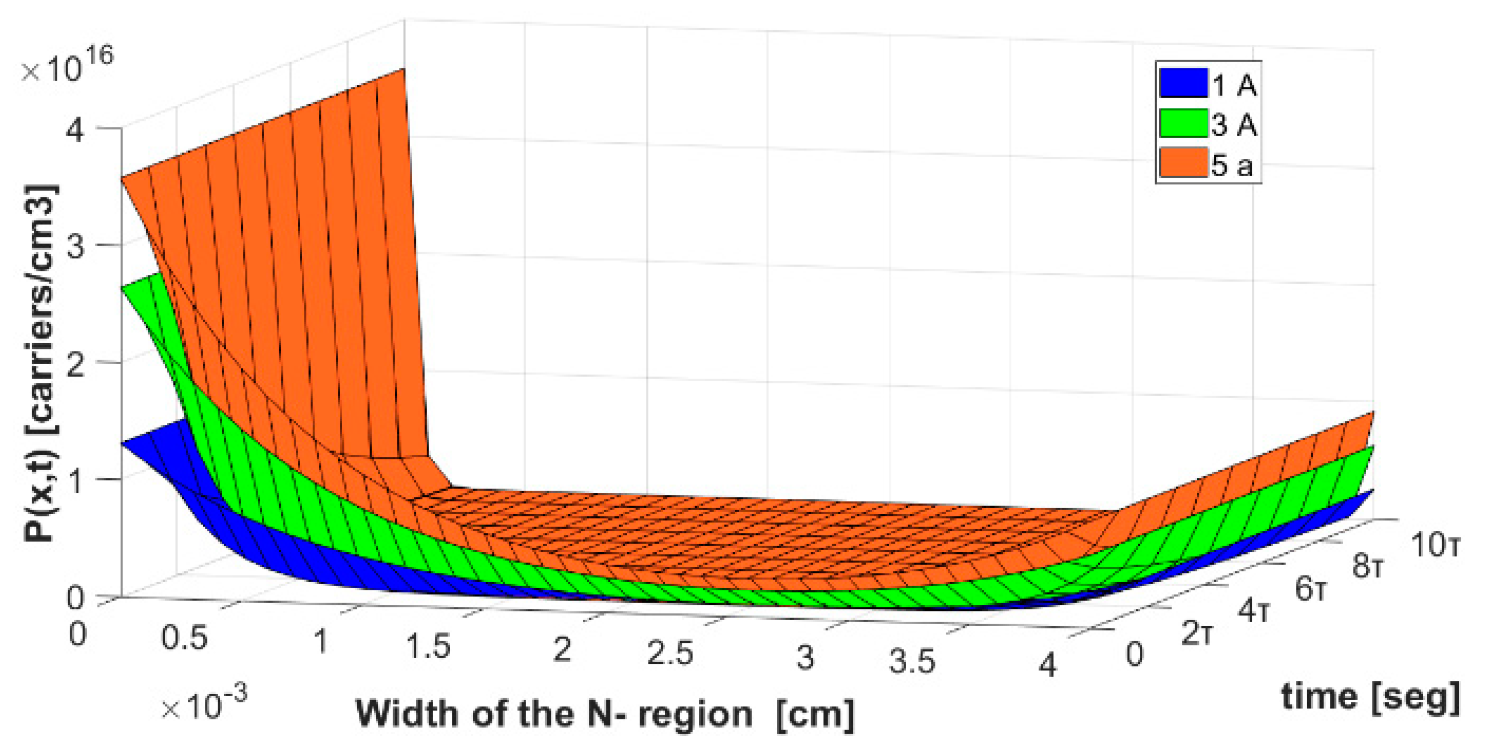
Figure 13 shows the p(x,t) evolution for a time range from 2τ to 10τ for a maximum current injection of 1 A, 3 A, and 5 A during the reverse blocking phase.
As shown in Figure 5, Figure 6, Figure 7, Figure 8, Figure 9, Figure 10, Figure 11, Figure 12 and Figure 13, the proposed ADE solution allows modeling the carrier’s injection behavior and the carrier’s evacuation in the N-region.
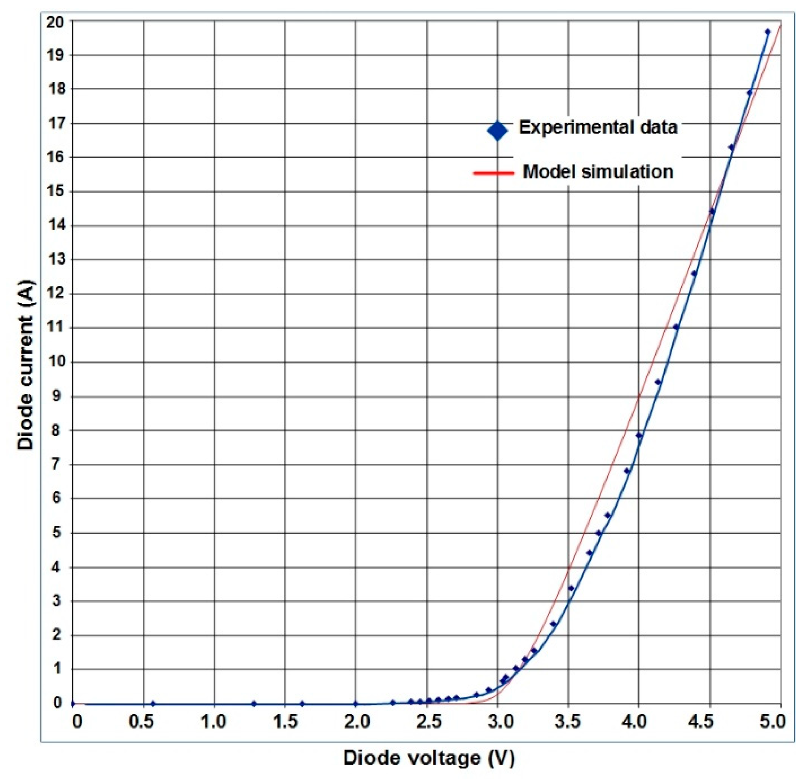
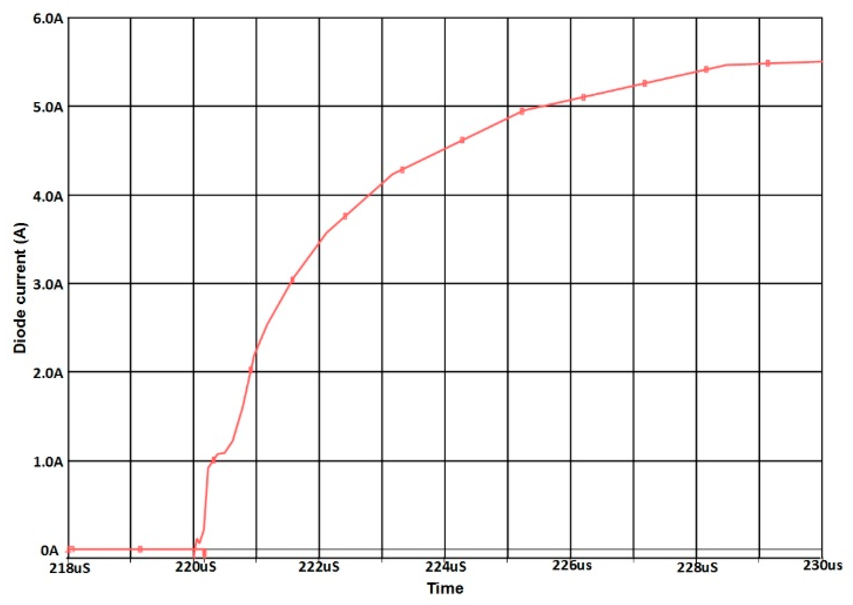
The proposed solution for modeling the chargers’ behavior in the N-region in a bipolar semiconductor device was used in the Orcad Pspice electrical circuit simulator, which allows the developed equations to be implemented easily, the characteristics are very similar to other simulators, and it is one of the simulators with greater acceptance and use in the electric area. The main results for the static, activation, and reverse blocking phases are shown in Figure 14, Figure 15 and Figure 16, respectively.
A straight comparison between the simulation and experimental results is presented to validate the proposed model obtaining similar current waveforms under static, turn-on, and turn-off conditions. As presented in the comparison of simulation results with the experimental data, adequate similarity was achieved for each phase of semiconductor device activation, which ensures a suitable model for use as a design tool prior to the realization of the experimental prototype.
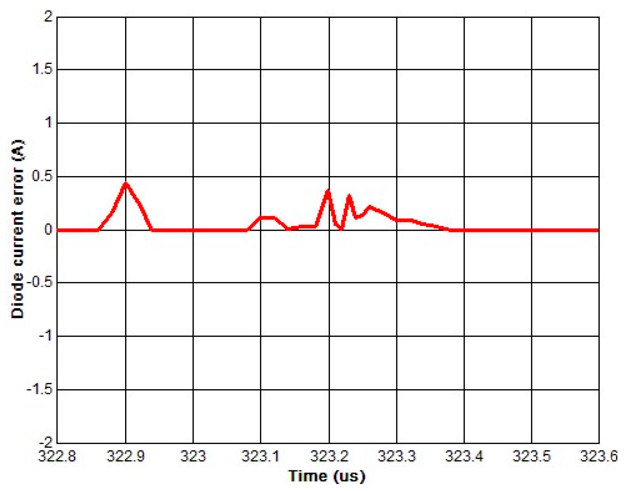
In this paper, an empirical approximation of the ADE solution is presented, and its final equation was validated via a commercial electronic circuit simulator. To quantify the accuracy of the obtained results, the quadratic error was evaluated by Equation (40) for the turn-off phase, which is considered the most unstable due to its negative current impulse. Figure 17 shows the quadratic error between the experimental and simulated waveforms.
e r r o r ( n ) = [ E x p ( n ) S i m ( n ) ] 2
where n is a sample of time; error(n) is the quadratic error; and Exp(n) and Sim(n) are the experimental and simulation sampled data, respectively.
Additionally, the mean square error (MSE) was obtained with Equation (41), and the obtained value was 0.0620 for the turn-off phase.
M S E = 1 i n = 1 i [ E x p ( n ) S i m ( n ) ] 2
where i is the number of samples.

5. Conclusions

An ambipolar diffusion equation solution using an empirical methodology was presented; this allowed for an adequate modeling of the injection and evacuation of carriers in the N-region. The method considers the main transport phenomena in the semiconductor material.
The proposed solution was validated using the final equations that were implemented in a simulator; the results were compared with experimental results in each phase, obtaining a similarity in the current waveforms.
An advantage of the proposed methodology is that the final expressions obtained can be easily implemented in any of the commercial simulators that has the option to integrate equations.
Finally, the proposed methodology was initially used in the pn junction, but it can be implemented in bipolar current control devices such as the BJT, IGBT, and thyristor family.

Author Contributions

Conceptualization, L.H.-G. and J.R.-H.; Data curation, J.R.-H. and O.U.J.-S.; Formal analysis, L.H.-G., J.R.-H. and M.A.O.-R.; Funding acquisition, L.H.-G., J.R.-H. and O.U.J.-S., Investigation, M.A.O.-R., R.B.S. and R.d.P.G.D., Methodology, L.H.-G. and M.A.O.-R., Project administration, L.H.-G.; Resources, J.R.-H. and O.U.J.-S.; Software, L.H.-G. and J.R.-H.; Supervision, L.H.-G.; Validation, J.R.-H. and O.U.J.-S.; Visualization, L.H.-G., J.R.-H. and O.U.J.-S.; Writing, original draft, L.H.-G., J.R.-H. and M.A.O.-R., Writing, review and editing, J.R.-H. and M.A.O.-R. All authors have read and agreed to the published version of the manuscript.

Funding

This research was funded by the Instituto Politécnico Nacional.

Institutional Review Board Statement

Not applicable.

Informed Consent Statement

Not applicable.

Data Availability Statement

Not applicable.

Acknowledgments

The authors are grateful to the Instituto Politécnico Nacional (IPN) for their encouragement and kind economic support to realize the research project.

Conflicts of Interest

The authors declare no conflict of interest.

Nomenclature

AActive area
ADEAmbipolar diffusion equation
B = µn/µpMobility relation
BJTBipolar Junction Transistor
DAmbipolar diffusion constant.
DnAmbipolar diffusion constant for electrons
DpAmbipolar diffusion constant for holes
EElectric field
EgBandgap
error(n)Quadratic error
Exp(n)Sampled Experimental data
Gn,pGeneration rate of electrons and holes
IGBTInsulated-Gate Bipolar Transistor
In(0,t)Electron current injected in the union P+N-.
In_driftElectron drift current
In(WB,t)Electron current injected in the union N-N+.
In_difusionElectron diffusion current
Ip(0,t)Hole current injected in the union P+N-
Ip_drifHole drift current
Ip(WB,t)Hole current injected in union N-N+
Ip_difusionHole diffusion current
ITD(x,t)Total injected current in the diode
IT_driftTotal drift current in the diode
LonAmbipolar diffusion lengthen in turn-on phase
LoffAmbipolar diffusion length in turn-off phase
LSAmbipolar diffusion length in static phase
MSEMean Square Error
niIntrinsic concentration.
nP+Electron concentration in the region P+
n(x,t)Electron concentration in the region N- in function of space and time
Px=0Initial concentration close to the union P+N-
Px=WBInitial concentration close to the union N-N+
p(x,t)Hole concentration in the region N- in function of space and time
Sim(n)Simulated sampled data
WBLow doping region width
VnElectron drift velocity
VpHole drift velocity

References

  1. Sze, S.M.; Kwok, K. Ng. p-n Juntion Diode. In Physics of Semiconductor Devices, 2nd ed.; Laboratories, B., Ed.; Wiley: New York, NY, USA, 1981; pp. 64–84. [Google Scholar]
  2. Neamen, D.A. The pn Juntion. In Semiconductor Physics and Devices, 3rd ed.; McGraw Hill: New York, NY USA, 2003; pp. 238–268. [Google Scholar]
  3. Liang, Y.; Gosbell, V.J. Diode Forward and Reverse Recovery Model for Power Electronic SPICE Simulations. IEEE Trans. Power Electron. 1990, 5, 346–356. [Google Scholar] [CrossRef]
  4. Chibante, R.; Araujo, A.; Carvalho, A. A new approach for physical-based modelling of bipolar power semiconductor devices. Solid-State Electron. 2008, 52, 1766–1772. [Google Scholar] [CrossRef]
  5. Sttrollo, A.G.M.; Napoli, E. Improved PIN diode circuit model with automatic parameter extraction technique. IEE Proc. Circuit Devices Syst. 1997, 144, 329–334. [Google Scholar] [CrossRef]
  6. Maxim, A.; Andreu, D.; Boucher, J. A new SPICE behavioral macromodeling method of magnetic components including the self-heating process. In Proceedings of the 30th Annual IEEE Power Electronics Specialists Conference, Charleston, SC, USA, 27 June–1 July 1999; pp. 735–740. [Google Scholar]
  7. Maxim, A.; Maxim, G. A novel power PIN diode behavioral SPICE macromodel including the forward and reverse recoveries and the self-heating process. In Proceedings of the IEEE Applied Power Electronics Conference and Exposition, New Orleans, LA, USA, 6–10 August 2002; pp. 1088–1094. [Google Scholar]
  8. Zhang, H.; Pappas, J.A. A Moving Boundary Diffusion Model for PIN Diodes. IEEE Trans. Magn. 2001, 37, 406–410. [Google Scholar] [CrossRef]
  9. Petzoldt, J.; Reimann, T.; Lorentz, L.; Zverev, I. Influence of device and circuit parameters on the switching losses of an ultra fast CoolMOS/SiC-diode device-set: Simulation and measurement. In Proceedings of the 13th International Symposium on Power Semiconductor Devices & ICs, Osaka, Japan, 4–7 June 2001; pp. 187–190. [Google Scholar]
  10. McNutt, T.R.; Hefner, A.R.; Mantooth, H.A.; Duliere, J.L.; Berning, D.W. Parameter Extraction Sequence for Silicon Carbide Schottky, Merged Pin Schottky, and Pin Power Diode Models. In Proceedings of the IEEE Power Electronics Specialists Conference, Cairns, QLD, Australia, 23–27 June 2002; pp. 1269–1276. [Google Scholar]
  11. McNutt, T.; Hefner, A.; Mantooth, A.; Berning, D.; Singh, R. Compact models for silicon carbide power devices. Solid-State Electron. 2004, 48, 1757–1762. [Google Scholar] [CrossRef]
  12. Levinshtein, M.E.; Mnatsakanov, T.T.; Ivanov, P.A.; Singh, R.; Palmour, J.W.; Yurkov, S.N. Steady-state and transient characteristics of 10 kV 4H-SiC diodes. Solid-State Electron. 2004, 48, 807–811. [Google Scholar] [CrossRef]
  13. Giesselmann, M.; Edwards, R.; Bayne, S.; Kaplan, S.; Shaffer, E. Forward and Reverse Recovery Spice Model of a JBS Silicon Carbide Diode. In Proceedings of the IEEE Twenty-Sixth International Power Modulator Symposium, San Francisco, CA, USA, 23–26 May 2004; pp. 364–367. [Google Scholar]
  14. Loulo, M.; Abdelkrim, M.; Gharbi, R.; Fathallah, M.; Pirri, C.F.; Tresso, E.; Tartaglia, A. Modelling and analysis of a-SiC:H p–i–n photodetectors: Effect of hydrogen dilution on dynamic model. Solid-State Electron. 2007, 51, 1067–1072. [Google Scholar] [CrossRef]
  15. Kolessar, R.; Nee, H.-P. A New Physics-Based Circuit Model for 4H-SIC Power Diodes Implemented in SABER. In Proceedings of the IEEE Applied Power Electronics Conference and Exposition, Anaheim, CA, USA, 4–8 March 2001; pp. 989–994. [Google Scholar]
  16. Hatakeyama, T.; Nishio, J.; Ota, C.; Shinohe, T. Physical Modeling and Scaling Properties of 4H-SiC Power Devices. In Proceedings of the IEEE International Conference on Simulation of Semiconductor Processes and Devices, Tokyo, Japan, 8–11 September 2005; pp. 171–174. [Google Scholar]
  17. Vogler, T.; Schroder, D. A New Accuracy Circuit-Modelling Approach for the Power Diode. In Proceedings of the IEEE Power Electronics Specialists Conference, Toledo, Spain, 29 June–3 July 1992; pp. 870–876. [Google Scholar]
  18. Metzner, D.; Vogler, T.; Schroder, D. A modular Concept for the Circuit Simulation of Bipolar Power Semiconductor. Trans. Power Electron. 1994, 9, 506–513. [Google Scholar] [CrossRef]
  19. Ma, C.L.; Lauritzen, P.O. A simple power diode model with forward and reverse recovery. In Proceedings of the IEEE Power Electronics Specialists Conference, Cambridge, MA, USA, 24–27 June 1991; pp. 411–415. [Google Scholar]
  20. Kraus, R.; Hoffmann, K.; Mattausch, H.J. A precise Model for the Transient Characteristics of Power Diodes. In Proceedings of the IEEE Power Electronics Specialists Conference, Toledo, Spain, 29 June–3 July 1992; pp. 863–869. [Google Scholar]
  21. Igic, P.M.; Mawby, P.A.; Towers, M.S.; Batcup, S. New physically-based PiN diode compact model for circuit applications. IEEE Proc. Circuit Devices Syst. 2002, 149, 257–263. [Google Scholar] [CrossRef]
  22. Carvalho, A.; Araujo, A.; Martins de Carvalho, J.L. A New Method for Solving the Ambipolar Diffusion Equation (ADE) Based on a Finite Element Formulation. In Proceedings of the Portuguese Conference on Automatic Control, Porto, Portugal, 15–17 September 1996. [Google Scholar]
  23. Manhong, Z. A modified finite difference model to the reverse recovery of silicon PIN diodes. Solid-State Electron. 2020, 171, 107839. [Google Scholar]
  24. Bryant, A.T.; Palmer, P.R.; Santi, E.; Hudgins, J.L. A Compact Diode Model for the Simulation of Fast Power Diodes including the Effects of Avalanche and Carrier Lifetime Zoning. In Proceedings of the IEEE Power Electronics Specialists Conference, Recife, Brazil, 12–16 June 2005; pp. 2042–2048. [Google Scholar]
  25. Liqing, L.; Angus, B.; Palmer, P.R.; Santi, E.; Hudgins, J.L. Physical Modeling of Fast p-i-n Diodes with Carrier Lifetime Zoning, Part I Device Model. IEEE Trans. Power Electron. 2008, 23, 189–197. [Google Scholar]
  26. Hernandez, L.; Claudio-Sanches, A.; Rodriguez, M.A.; Ponce-Silva, M. Physical Modeling of SiC Power Diodes with Empirical Approximation. J. Power Electron 2011, 11, 381–388. [Google Scholar] [CrossRef] [Green Version]
  27. Dyakonova, N.V.; Ivanov, P.A.; Kozlov, V.A.; Levinshtein, M.E.; Palmour, J.W.; Rumyantsev, S.L.; Singh, R. Steady-State and Transient Forward Current-Voltage Characteristics of 4H-Silicon Carbide 5.5. kV Diodes at High and Superhigh Current Densities. Trans. Electron. Devices 1999, 46, 2188–2193. [Google Scholar] [CrossRef]
Figure 1. Charge distribution in the N-region.
Mathematics 09 00458 g001
Figure 2. Carriers installation in the N-region, in the activation phase.
Mathematics 09 00458 g002
Figure 3. Lon(t) response.
Mathematics 09 00458 g003
Figure 4. Loff(t) response.
Mathematics 09 00458 g004
Figure 5. p(x) response in the static phase.
Mathematics 09 00458 g005
Figure 6. QB response in function of the injected current.
Mathematics 09 00458 g006
Figure 7. N-region resistance and injected current relation.
Mathematics 09 00458 g007
Figure 8. Q(t) behavior during the conduction phase.
Mathematics 09 00458 g008
Figure 9. p(x,t) behavior during the conduction phase.
Mathematics 09 00458 g009
Figure 10. p(x,t) behavior for 5 A, 3 A, and 1 A.
Mathematics 09 00458 g010
Figure 11. Qoff behavior during the reverse blocking phase for different carriers’ evacuation.
Mathematics 09 00458 g011
Figure 12. p(x,t) behavior during the reverse blocking phase.
Mathematics 09 00458 g012
Figure 13. p(x,t) for 5 A, 3 A, and 1 A during the reverse blocking phase.
Mathematics 09 00458 g013
Figure 14. Static simulation and experimental data.
Mathematics 09 00458 g014
Figure 15. Turn-on phase simulation results.
Mathematics 09 00458 g015
Figure 16. Turn-off simulation and experimental data.
Mathematics 09 00458 g016
Figure 17. Turn-off phase error.
Mathematics 09 00458 g017
Table 1. Injected current vs. P0 and PW.
Current [A]P0 [Charges/cm3]PW [Charges/cm3]
0.58.043 × 10151.384 × 1015
11.310 × 10162.571 × 1015
1.51.712 × 10163.627 × 1015
22.056 × 10164.588 × 1015
2.52.362 × 10165.476 × 1015
32.640 × 10166.305 × 1015
3.52.897 × 10167.085 × 1015
43.137 × 10167.824 × 1015
4.53.362 × 10168.529 × 1015
53.576 × 10169.203 × 1015
Publisher’s Note: MDPI stays neutral with regard to jurisdictional claims in published maps and institutional affiliations.