Abstract
While integrated circuit technologies keep scaling aggressively, analog, mixed-signal, and radio-frequency (RF) circuits encounter challenges by creating robust designs in advanced complementary metal–oxide–semiconductor (CMOS) processes with the diminishing voltage headroom. The increasing random mismatch of smaller feature sizes in leading-edge technology nodes severely limit the benefits of scaling for (RF)/analog circuits. This paper describes the details of the combinatorial randomness by statistically selecting device elements that relies on the significant growth in subsets number of combinations. The randomness can be utilized to provide post-manufacturing reconfiguration of the selectable circuit elements to achieve required specifications for ultra-low-power systems. The calibration methodology is demonstrated with an ultra-low-voltage chaos-based true random number generator (TRNG) for energy-constrained Internet of things (IoT) devices in the secure communications.
1. Introduction
Although the CMOS technology reaches the deep-submicron regime, performance of digital circuits follows the prediction of Moore’s Law in the past decades. Performance of leading microprocessor doubles approximately every 18 months [1]. However, analog, mixed-signal circuits, and radio-frequency (RF) circuits are left far behind this trend. For example, performance of analog-to-digital converters (ADCs) takes 6.5 years to double [2]. Even the leading ADCs have a slightly faster progress rate of doubling every 4.7 years. Obviously, the RF and analog circuits are not able to take full advantage of process progress. Even the analog circuits cannot fully benefit from the technology scaling, analog circuits still play the quintessential role of interfacing digital signal processors to analog physical world in almost every electronic device, especially in the billions of Internet of things (IoT) devices. Challenges in the nano-meter scale would be even more rigid for RF/analog circuits since the power supply voltages decrease. Although threshold voltages in the advanced technology reduce as well, the available voltage headroom for these complicated mixed-signal functions still degrades rapidly. Besides, the problem of process variations is another challenge for robust design of RF/analog circuits due to aggressive technology scaling. In order to address matching issues in the nano-scale technology nodes, conventional sizing methods [3] that adopt large-size transistors for RF/analog circuits is still very popular even in advanced complementary metal–oxide–semiconductor (CMOS) processes. Although many of systematic variations can be predicted and tackled by utilizing careful circuit and layout techniques. The problems of large random variations are still needed to be addressed with alternate methods other than conventional up-sizing methods. The redundancy method [4] was proposed to address this issue and demonstrated in flash ADC designs. To achieve a better energy efficiency, statistical element selection (SES) [5,6] was proposed to exploit the combinations of random mismatches. In this paper, the combinatorial randomness will be utilized to efficiently the exploits subcomponents of the input differential pairs in the analog amplifiers to mitigate the impact of the process variations. A design example of a chaos-based true random number generator (TRNG) will be presented to demonstrate how the combinatorial randomness can be adopted to reduce the power consumption while the circuit is operating at ultra-low power supply voltage.
The remainder of this paper is organized as follows. Section 2 reviews the primary sources of random variations in advanced CMOS technology nodes and the effects RF/on analog circuits. In Section 3, the combinatorial randomness methodology that statistically selects circuit elements is analyzed in detail for the implementation of RF/analog circuits. A chaotic true random number generator (TRNG) for hardware security that demonstrates the potential for improved power efficiency with the combinatorial randomness is discussed in Section 4, and finally, the conclusions are drawn in Section 5.
2. Process Variations in CMOS Processes
2.1. Process Variations
In advanced CMOS technology nodes, the process variations are a significant problem and will become more serious in more advanced nodes. The process variations that might come from layout dependent effects or across-field effects result in the systematic variations [7]. For example, the threshold voltage of a metal–oxide–semiconductor field-effect transistor (MOSFET) far away from n-wells would be different from an identical one that is close to an n-well. The well proximity effect and other issues such as the polysilicon surrounding of the gates and shallow trench isolation (STI) stress [8,9,10] lead to the layout-dependent systematic variations of different characteristics for identical devices in the wafer. The other major source that results in systematic variations is the across-field effects that are due to lithography or etching. The location of different dies on the same wafer can result in a systematic offset in device characteristics although devices in the same vicinity would have the same effects on them. Through careful circuit and layout techniques, most of the systematic variations can be alleviated. Moreover, more and more restricted design rules in advanced CMOS technology nodes, such as single poly orientation, fixed gate lengths, and high regularity in the physical layers, are adopted to mitigate those systematic variations [11,12]. Emerging lithography and etching solutions, such as optical proximity correction and double patterning, are also used to provide better matching for leading-edge CMOS nodes.
On the contrary, random variations that are due to unpredictable and unrepeatable variations in manufacturing, such as random dopant fluctuation (RDF) in the transistor channel [13] and line edge roughness (LER) can result in uneven channel length in the poly line forming the gate across the width of the device and cause significant mismatch in the conductance constant among devices on the same die. Although many novel technologies have been proposed to address such problems including high-k metal gates, undoped channels, thin silicon-on-insulator devices, and Fin-FETs, threshold voltage variation in tens of milli-volts of is still expected [14,15,16,17,18].
2.2. Popular Methods for Mismatch Calibration
To reduce the local random mismatch, the traditional approach following Pelgrom’s seminal paper [3] is sizing up the device size because the standard deviation of random mismatch is inversely proportional to the square root of the device area. Figure 1 shows a typical circuit diagram of a comparator, which is called StrongArm comparator. The standard deviation of input offset voltage for the differential pair is characterized by Pelgrom in [3] as:
where AVT and Aβ are process-related coefficients, W and L are width and length of the differential pair. Assuming that the input offset voltages of the differential pair is the dominant sources of variations, the intuitive approach to reduce the offset voltages is to increase the device area. It means increasing area and current can lead to improved matching. With up-sized devices, the power consumption increases due to the larger current. Moreover, due to larger device loading capacitance and its parasitic capacitance, the required power would be increased further to achieve the bandwidth target. Hence, the power consumption is challenging for RF/analog circuits in advanced CMOS technology nodes even the devices can have higher operation speed. The problem is even worse while higher resolutions are required because the specifications rapidly increases the number of elements that need better matching.
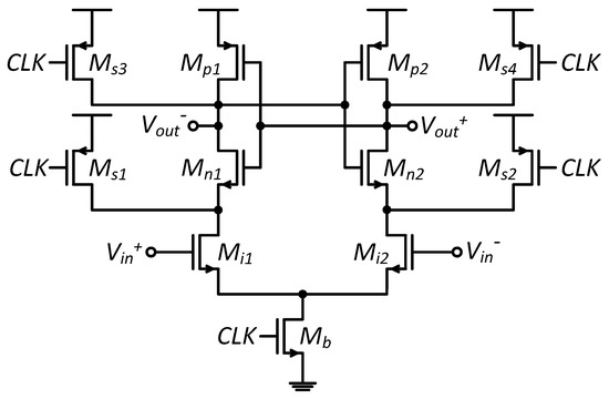
Figure 1.
A typical structure of a comparator.
Redundancy was proposed to achieve a better tradeoff between power consumption and device mismatch and demonstrated for flash ADCs in [4,19,20,21] with extra comparators to be able to select the best offset voltages of 2N comparators for an N-bit design. Instead of putting one comparator for one comparison level, adding extra comparators to each level is implemented in the N-bit flash ADC, as shown in Figure 2. The calibration incorporating redundancy is to select and reassign the best comparators with the minimum offset for an N-bit design. If the standard deviation of comparator offset is at the order of 1 LSB, the probability distribution functions (PDFs) of the comparator offset will overlap with neighboring comparators. The comparator can be reassigned with the overlapping PDFs, which means a comparator nominally designed for one reference level can be used as another comparison level. For example, in Figure 2 comparator 2a can be used to represent Level 4 after fabrication. By utilizing the large number of redundancy comparators, this approach highly increases the probability that at least one comparator can satisfy the matching specification with a small area. However, the redundant comparators still occupy a large area although the unused comparators can be disabled and do not contribute power consumption.
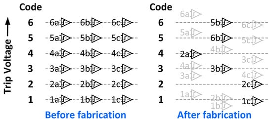
Figure 2.
Comparator redundancy that chooses one of implemented comparators after fabrication for each comparison level.
The other method to achieve better tradeoff between power consumption and device matching for an input differential pair in comparators, the digital calibration digital-to-analog converters (DACs) is also very popular in advanced CMOS processes. DAC-based calibration can be implemented by adding a current DAC tapping to the drain nodes of the input differential pair as shown in Figure 3a [22]. The overhead of the current DAC can be very low and it injects current to change the offset voltage to achieve better matching. The internal nodes can be also adjusted with digitally controlled capacitive DACs [23], as shown in Figure 3b. The capacitor mismatch is added to the signal path to create a slight imbalance that results in an offset voltage. Therefore, the random offsets can be cancelled with the capacitive DAC. Meanwhile, the capacitive DACs can further create a systematic offset to eliminate the requirement of the reference ladder. However, the dynamic mismatch errors that occur during high speed operation cannot be characterized with this methodology.
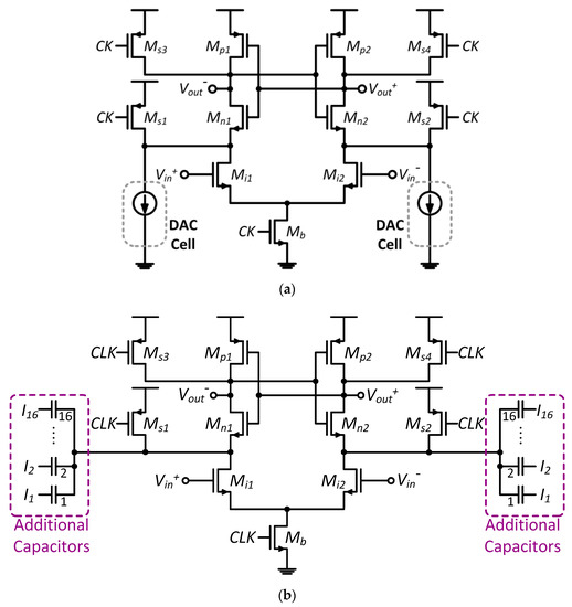
Figure 3.
(a) Current digital-to-analog converter (DAC) calibrated comparator, and (b) offset calibration with capacitive DACs.
In the more advanced CMOS nodes, the digital calibration with DACs and redundancy methods require significant overhead costs due to more serious problems of the random mismatch. Therefore, statistical element selection (SES) was proposed to mitigate the impact of extreme random variability through the implementation of combinatorial redundancy [5]. By choosing one subset from available subsets, each component in RF/analog circuits requiring better matching property is formed from N identically-designed subcomponents. For example, the input differential pair in a comparator is formed from a group of elemental pairs. For redundancy methodology, only one branch is selected individually. However, the digitally enabling selection of subcomponents, the combinatorial randomness can be implemented very efficiently. The search space of combinatorial randomness with statistical selections is much larger than using traditional redundancy methods because the exponential increase in the number of combinations leads to a significant improvement in probability to achieve the targeted matching specification at the little increased cost of statistical selection. In the following session, the combinatorial randomness with statistical element selection is discussed in more details.
3. Combinatorial Randomness
3.1. Expliotion of Random Mismatch
The basic concept of combinatorial randomness is to select a combination of identically designed elements for a critical circuit block, so it chooses one subset from the available subsets to meet the required specification. For example, a subset branch of input transistor pairs in an amplifier is selected to have a small input offset voltage, as shown in Figure 4 [5]. The differential amplifier with combinatorial randomness is composed of N pairs of input N-type metal-oxide-semiconductor (NMOS) transistors labeled as through and selection NMOS transistors with gates tied to digital control signals through . Each input pair can be selected by turning on or off with . Due to the random variations, each transistor would show different characteristics and, hence, the mismatches between the different input pairs leads to input offset voltages.
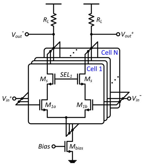
Figure 4.
Radio-frequency (RF)/analog differential amplifier with combinatorial randomness.
The aforementioned up-sizing approach based on the Pelgrom model and the redundancy methodology can be viewed as two extreme cases of the element selections. To realize the Pelgrom approach, all pairs from 1 to N are selected. Therefore, a lower effective variation can be achieved by utilizing the larger area by the selection of all branches, and the matching standard deviation can be improved by . To implement the redundancy approach, input pairs are grouped into predetermined identical blocks, and only one block is selected for each comparison level during post-manufacturing configuration. For example, the pair in Figure 4 with the best offset result is selected if one pair is predetermined to form one block and total number of selectable blocks is N. If pairs are predetermined to form one block, only two combinations cab be selected after manufacturing.
To achieve finer resolution, the presented methodology can individually select each element by using the efficient digital selection rather than grouping the elements into predetermined blocks. Therefore, the search space is much larger than that of the redundancy methodology described in [4]. Subsets can be selected by using the digital control signals if pairs are desired. If eight pairs are used to form a block from total 16 pairs, only two blocks can be used for selection with one redundancy element. A total 12,870 combinations, however, are available if any subset of eight elements can be selected. Moreover, the size of combinatorial subset is not limited to , and any size of the subset from one to N can be used for selection, Therefore, total combinatorial subsets can be selected. The exponential increase in the number of total available combination subsets lead to a significant improvement in successfully finding a combination subset that can meet the desired specification.
For the differential amplifier as shown in Figure 4, the transconductances of all pairs are assumed to be the same. The overall input offset voltage of the differential amplifier can be expressed as:
where is the input offset voltage of the ith input pair. If the case of that only a subset selected from the N pairs is considered, the resulting input offset voltage equals to:
where if the ith pair is chosen, and otherwise.
Because the input offset voltage of the differential pair is generally dominated by the mismatch of threshold voltages, , the input offset can be expressed as [24]. Moreover, the input transistors are usually the dominant source of threshold voltage mismatch, so the input offset voltage of the differential amplifier can be determined to be , where by using (3) and assuming that the distribution of is a Gaussian normal distribution with . It means that the overall offset voltage is smaller if more elements are selected, so matching of devices in proximity can be improved by . The result matches was found by Pelgrom in [3]. To meet a desired specification such as a small input offset voltage with high probability like 99.5% with lowest possible power and area, some parameters, such as total number of elements selected (k) from selectable elements (N) and the size of each element, are required to be determined. Hence, the total number of sets among and needed calibration time can be calculated. The methodology to determine the parameters is described in the following section.
3.2. Methodology of Combinatorial Randomness
Figure 5 shows a latch type comparator with combinatorial randomness that is used in a flash type ADC and the dark sections are replicated N times [5]. Only one element among the N selectable elements that have an offset distribution of normal distribution is selected. Hence, the probability that the offset voltage smaller than a given specification spec of one element can be expressed as:
where is the probability that the offset voltage of the element falls out of the given offset range (spec). For the comparators in a flash type ADC, spec should be less than ±0.5LSB to ensure good linearity. Because the offset voltage of each element is independent, the probability that the offset voltage of every element falls out of the given offset range can be calculated as:
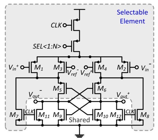
Figure 5.
Latch type comparators with combinatorial randomness.
Equation (5) can be viewed as the case of the redundancy approach with N redundant elements. If all N elements are selected, the distribution of the offset voltage follows , and the probability that the offset is within spec can be calculated by substituting in (4) with . This case can be viewed as up-sizing method for reduction of random variability. Both approaches are the two extremes for combinatorial randomness by selecting one at a time (redundancy), or all at once (up-sizing).
Combinatorial randomness selects k elements among N selectable ones at a time (). To show the efficiency of the presented methodology, the failure probability () for different values of k is simulated with , and offset specification (spec) is by using Monte Carlo samples in MATLAB in Figure 6 [5]. The failure probability, , that an absolute offset voltage of each element is larger than 1/100 of the standard deviation can be calculated from (4) using and .
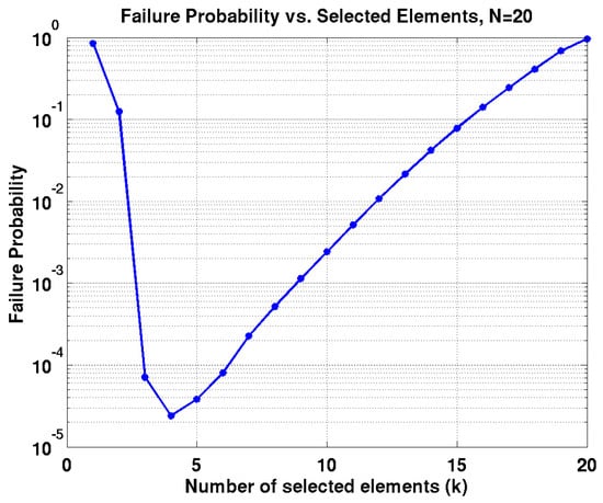
Figure 6.
Failure probability for , , .
The up-sizing method can correspond to the rightmost point in the contour where all the 20 elements are select and only one subset is available (select all elements, ). The failure probability for this subset with the up-sizing method can be calculated from (4) with and because the standard deviation decreases by according to the result in [3]. The failure probability of the up-sizing method is simply because there is only one subset of 20 elements. The leftmost corresponds to the case with redundant elements and 20 independent subsets of only one element each () are available for selection. The failure probability of the redundancy approach can be calculated by . The failure probability of the combinatorial randomness is much lower than both redundancy and up-sizing approaches by several orders of magnitude if k is chosen between these two extremes, i.e., . While both N and k are varied, the failure probability of the combinatorial randomness is shown in Figure 7 [5], where each blue contour corresponds to a different N value (). The x-axis shows the number of the selected elements (k) among N selectable ones (). Each selectable element is assumed to follow and . The appropriate pair of N and k can be searched for a specific while the highest ratio for each k can be reached to reduce the parasitic loading, as shown in Figure 7 with red circles for each k.
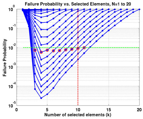
Figure 7.
Failure probability for , , .
The comparison of abovementioned methods is shown in Figure 8 as normalized area is varied [5]. With Monte Carlo simulation with 10,000 samples in MATLAB, the yield for different methods can be estimated assuming that the offset voltage of each selectable element follows a normal distribution with . The yield for DAC-based calibration is:
where is the calibration step size, and n is the resolution of the calibration DAC [25]. Significant improvement in success probability can be achieved with combinatorial randomness compared to the other methods.
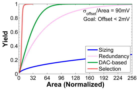
Figure 8.
Comparison of statistical element selection (SES), redundancy, scaling and DAC-based calibration.
4. Combinatorial Randomness Applications in RF/Analog Integrated Circuit Design for Hardware Security in Energy-Constrained Devices
4.1. In-Sensor Encryption with Reconfigurable Chaotic Systems
In the near future, the number of Internet of things (IoT) devices is expected to grow into billions that leads to revolutionize various applications, such as pervasive environmental sensing and continuous health monitoring. Particularly, with the extensive use of the radio-frequency identification (RFID) systems, many non-electronic objects could be turned into a wireless network of IoT sensors. Wireless connection increases the communication efficiency between pervasive sensors and the cloud [26,27,28,29]. Unfortunately, cyberattacks also increase due to a large amount of entry points in the network. Although software security patches can be used to fix vulnerabilities, users usually do not install them immediately. Devices lacked of physical un-clonable functions (PUF) can be attacked with inauthentic substitutions, physical tampering, and reverse engineering [30]. Side-channel analysis attacks are one of the typical attacks that analyze the hardware runtime characteristics, such as power consumption and electromagnetic wave, of a cryptographic device to obtain secret information [31]. For example, a strong advanced encryption standard (AES) key can be measured by correlation power analysis (CPA) [32]. Analog sensors not under the protection of crypto-enabled digital systems are particularly vulnerable to cyberattacks. For instance, an adversary may capture the confidential data and modify critical decisions [33,34]. Although advanced cryptographic algorithms can guarantee the integrity and confidentiality of sensor data [35], computation capabilities of sensors are constrained by a low power budget. Hence, a significant gap exists to integrate complete security measures into energy-constrained sensors. Recently, true random number generators (TRNGs) have been utilized as the important building block of many wireless networks with RFID systems. To enable cryptographic algorithms, random numbers play a critical role to generate encryption keys that need to be extremely resilient to the malicious attacks.
A sensor system with RFID is usually composed of a sensor front end, a transceiver, and a random number generator for data encryption, as shown in Figure 9. A strong encryption algorithm can prevent from an external attack. However, due to limited resources, such as power consumption, in wireless sensor networks for RFID wearable and implantable systems [36,37], pseudo-random number generators (PRNGs) were typically adopted instead of TRNGs for the simpler architecture. PRNG algorithms generate repeating random-like sequences with using an initial seed. Leaks of the random seed can make the PRNG outputs predictable [38]. Moreover, the PRNG output would be predictable if the internal state and the periodicity of the structure are known. On the contrary, TRNGs generate the random numbers from an observable activity or a physical process with true randomness. The conventional approach is power consuming because it requires a high-gain and wide-bandwidth amplifier to magnify the small noise voltages [39]. Utilizing energy harvested from an ambient environment to avoid frequent battery replacement provides a compelling solution for many distributed devices. However, the harvested power is limited and not stable while environmental conditions and energy sources vary. For example, energy harvested from thermoelectric generators (TEGs) is highly temperature dependent [40,41]. Therefore, the system for IoT applications to be powered by energy harvesters requires to consume very low power and operate at an ultra-low voltage of less than 0.5 V [41,42,43]. In addition, ubiquitous computing opens a new door for hackers to enter the central network through unprotected pervasive devices. Hence, the critical need is to integrate security measures into each connected device with minimum increase of power consumption. However, a gap exists to implement power-hungry advanced encryption standard (AES) in sensors. Moreover, to protect the key from being stolen through side-channel detection, advanced digital encryption may require additional circuits to shield fluctuations in the power source. On the other hand, the discrete-time chaos-based true random number generators (TRNGs) are not affected by statistics of the entropy source and resilient to the presence of the deterministic noise [44], which would be the promising security module that can be integrated onto resource-limited devices to provide complete security measures.
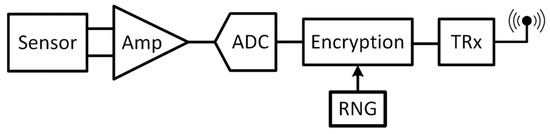
Figure 9.
The typical architecture of a wireless radio-frequency identification (RFID) sensor network with the random number generator for encryption.
4.2. Approach
Whitening the primary features is how creatures efficiently communicate and hide themselves from predators, which appears to be a ubiquitous property of nature. Such effective ways to encrypt the signal, also known as the phenomenon of Chaos, can as essentially be thought of as “deterministic noise”. Dynamics of discrete-time chaotic systems can be governed by nonlinear maps. Figure 10a shows the self-feedback discrete-time chaotic system with a piecewise linear map shown in Figure 10b. The output of the chaotic generator, , is connected to the input of the map function, , as next input . The transformation function, , is given as , where is equal to 1 when ; is equal to −1 when . “” is the maximum output voltage so that the output is bounded by and . Si is the signal to encrypt and it is sampled at fc, while is clocked at fs. When fs is several times higher than fc, the sampled signal will be scrambled and permutated in the loop. The dynamic signal evolves from the underlying principle of self-similarity at different scales, as shown in Figure 10b, where the orbit is generated from an initial condition of 0.7 with a gain close to 2 and as 0.5. Figure 10c shows the output signal is aperiodic and noise-like in time domain, while it is continuous and wideband in frequency domain. The state space trajectories originating from two closely spaced initial conditions diverge exponentially, showing high sensitivity to initial conditions, as shown in Figure 10d. Hence, different deterministic noises can be created with different initial inputs. With matched chaotic generators integrated in both sensors and receivers, the signals can be encrypted and decrypted in real time. Chaotic encryption can be performed before transmission via the edge node radio to produce a transformed waveform that is unintelligible. The receiving node correspondingly performs the converse decryption to recover the original signal, as shown in Figure 11a. The initial states and targeted maps can be setup through synchronization to ensure that two chaotic systems have the same trajectories. The chaotic generator can be realized with the topology similar to the residue amplifier in pipeline ADCs, where the parameter G represents gain, is the reference voltage, and is the offset voltage. To make the system more dynamic, multiple maps can be cascaded to increase the overall gain, as shown in Figure 11b,c. To avoid using power-hungry close-loop amplifiers, multiple-stage architectures using reconfigurable open-loop amplifiers can be utilized to increase the overall gain. The open-loop gain, G, is equal to transconductance, gm, times output impedance, ZL.
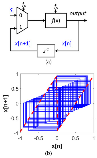
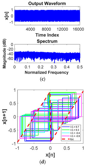
Figure 10.
(a) Self-feedback chaotic system; (b) trajectory with piecewise-linear map; (c) output signal (upper figure) and spectrum (lower figure); (d) orbits with different initial states.
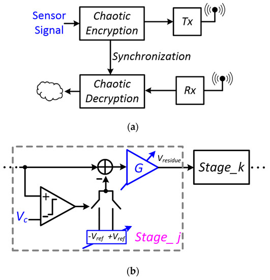
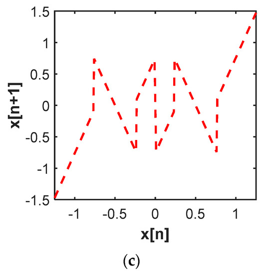
Figure 11.
(a) Chaotic encryption for Tx and Rx; (b) open-loop residue amplifier; (c) multi-stage transformation function.
In order to minimize power consumption, combinatorial randomness of intrinsic transconductance from minimum-sized devices will be deployed to provide maximum programmability, as shown in Figure 12a. Process variations result in a wide-range gm from the selectable devices, where the combinatorial gm can be characterized with decision windows to generate different gains for the transformation function. When signals propagate to the next stage, the first map will be reconfigured to ensure that the overall gain follows the dynamic law without interrupting its operation. Figure 12b shows the control loop to train the transformation function with different maps. The algorithm compares the Xref and Xtrained to update the selection of the combinatorial subset until the average of Xdiff is equal to zero. The transformation functions can be updated from time to time so that the signal can travel in time-varying orbits to enhance the strength of the security. Given that devices are with various intrinsic transconductances after fabrication, different subsets will be enabled for different devices. Hence, every device is unique so that it is inherently embedded with un-clonability. The reconfigurable chaotic system is expected to achieve sub-nW operations by exploring nonlinear dynamical effects and combinatorial intrinsic transconductance.
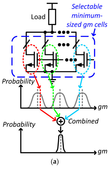
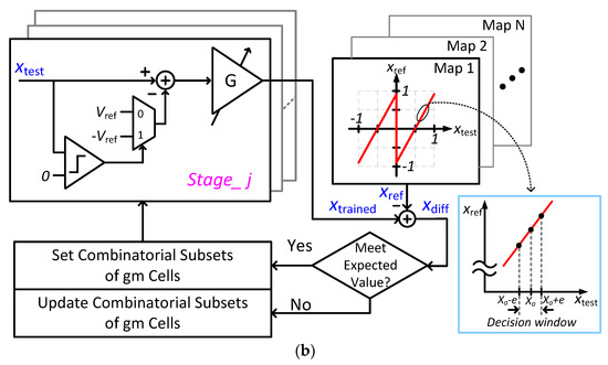
Figure 12.
(a) Utilization of the combinatorial intrinsic characteristics and (b) the training process with different maps.
4.3. Simulation Results
To assess the proposed reconfigurable chaotic system, we have created a compact simulation model of two-stage residue amplifiers based on physical characteristics and different noise levels. Each residue amplifier works at difference phase. As the simulation results shown in Figure 13a, the output signals appear to have the chaotic behavior with zero cross-correlation and impulse-like auto-correlation. To determine how often the chaotic systems need to be synchronized, the internal noise is set to different levels from 6-bit to 16-bit resolution, where the internal clock of the transformation function is 100 times of the input signal. Therefore, for each sampled data, the internal noise is integrated in the loop for one hundred cycles. Figure 13b shows that synchronization rate increases when the internal noise level is higher. For instance, with a 6-bit noise-level, the system needs to be synchronized every ten sampling periods, while with 16-bit resolution, the synchronization cycle extends to 20 sampling periods. The signal can be transformed effectively into deterministic noise without showing intelligible patterns on the power supply. Figure 13c illustrates unsuccessful CPA attacks on the proposed chaotic system with 50,000 traces. These simulation results demonstrate that this approach can counter side-channel attacks. With synchronization between two chaotic systems with combinatorial randomness, the decoded signal has been recovered with less than 1% performance degradation comparing to signals without being scrambled. This data confirms that the proposed approach for improving sensory-interface security with combinatorial randomness is feasible and effective.
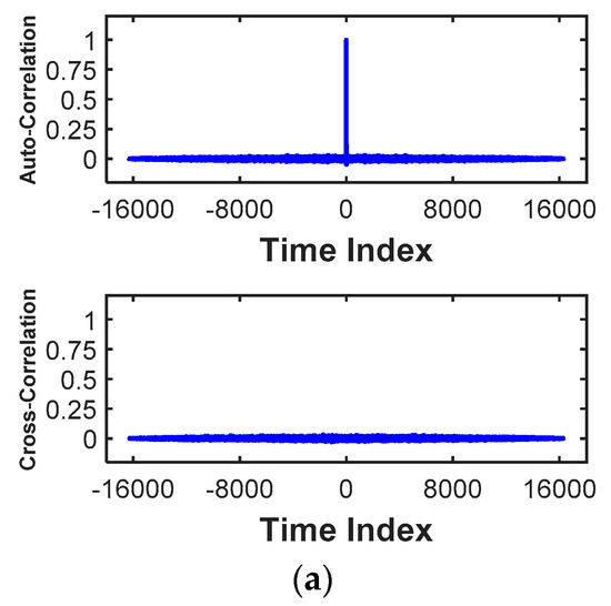
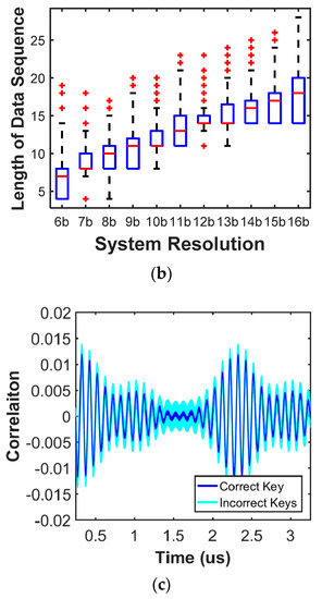
Figure 13.
(a) Upper figure illustrates auto-correlation and lower figure shows cross-correlation, (b) noise levels vs. synchronization rates (length of data), and (c) correlation power analysis (CPA) attacks with 50,000 traces.
5. Conclusions
A calibration methodology based on combinatorial randomness by statistically selecting elements offers an effective approach to mitigate random variation impact on mismatch. While combinatorial randomness has been demonstrated in this paper for comparator offset calibration in flash ADCs and differential pairs in chaos-based TRNGs, the approach can be generally applied to matching of any two or more components for integrated circuit design. The simulation results show that the combinatorial randomness approach for any matching design problem can achieve several orders of magnitude of improvement as compared to other calibration approaches. The fundamental analog differential amplifier validated the mathematical models, and the benefits from random process variations will be more prominent in more advanced technology nodes, such as 28 nm nodes and beyond. The efficacy of combinatorial randomness will increase while more effort is placed on the hardware-algorithm co-design of the integrated circuits.
Author Contributions
Conceptualization, E.C. and V.C.; methodology, E.C. and V.C.; software, E.C.; validation, E.C.; formal analysis, E.C. and V.C.; investigation, E.C.; resources, V.C.; data curation, E.C.; writing—original draft preparation, E.C.; writing—review and editing, V.C.; visualization, E.C.; supervision, V.C.; project administration, V.C.; funding acquisition, V.C. All authors have read and agreed to the published version of the manuscript.
Funding
This research was funded by the National Science Foundation CARRER program, grant number 1953801.
Conflicts of Interest
The authors declare no conflict of interest.
References
- Moore, G. No Exponential is forever: But ‘Forever’ Can Be Delayed! In Proceedings of the IEEE International Solid-State Circuits Conference Digest of Technical Papers, San Francisco, CA, USA, 13 February 2003. [Google Scholar]
- Murmann, B.; Boser, B.E. Digitally Assisted Pipeline ADCs; Springer: New York, NY, USA, 2004. [Google Scholar]
- Pelgrom, M.J.M.; Duinmaijer, A.C.J.; Welbers, A.P.G. Matching Properties of MOS Transistors. IEEE J. Solid-State Circuits 1989, 24, 1433–1439. [Google Scholar] [CrossRef]
- Flynn, M.P.; Donovan, C.; Sattler, L. Digital Calibration Incorporating Redundancy of Flash ADCs. IEEE Trans. Circuits Syst. II Analog Digit. Signal Process. 2003, 50, 205–213. [Google Scholar] [CrossRef]
- Chen, V.H.-C.; Keskin, G.; Pileggi, L.T. Self-Healing Circuits Using Statistical Element Selection. In Analog/RF and Mixed-Signal Circuit Systematic Design; Fakhfakh, M., Tlelo-Cuautle, E., Castro-Lopez, R., Eds.; Springer: Berlin/Heidelberg, Germany, 2013; pp. 53–75. [Google Scholar]
- Chen, V.H.-C.; Pileggi, L. A 69.5 mW 20 GS/s 6b Time-Interleaved ADC with Embedded Time-to-Digital Calibration in 32nm CMOS SOI. IEEE J. Solid-State Circuits 2014, 49, 2891–2901. [Google Scholar] [CrossRef]
- Agarwal, K.; Nassif, S. Characterizing process variation in nanometer CMOS. In Proceedings of the ACM/IEEE Design Automation Conference, New York, NY, USA, 4–8 June 2007. [Google Scholar]
- Scott, G.; Lutze, J.; Rubin, M.; Nouri, F.; Manley, M. NMOS drive current reduction caused by transistor layout and trench isolation induced stress. In Proceedings of the International Electron Devices Meeting (IEDM), Technical Digest, Washington, DC, USA, 5–8 December 1999. [Google Scholar]
- Fukutome, H.; Momiyama, Y.; Satoh, A.; Tamura, Y.; Minakata, H.; Okabe, K.; Mutoh, E.; Suzuki, K.; Usujima, A.; Arimoto, H.; et al. Carrier profile designing to suppress systematic variation related with device layout by controlling STI-enhanced dopant diffusions correlated with point defects. In Proceedings of the 2009 IEEE International Electron Devices Meeting (IEDM), Baltimore, MD, USA, 7–9 December 2009. [Google Scholar]
- Gupta, P.; Heng, F.-L. Toward a systematic-variation aware timing methodology. In Proceedings of the ACM/IEEE Design Automation Conference, San Diego, CA, USA, 7–11 June 2004. [Google Scholar]
- Webb, C. 45 nm design for manufacturing. Intel Technol. J. 2008, 12, 121–130. [Google Scholar]
- Jhaveri, T.; Rovner, V.; Liebmann, L.; Pileggi, L.; Strojwas, A.J.; Hibbeler, J.D. Co-optimization of circuits, layout and lithography for predictive technology scaling beyond gratings. IEEE Trans. Comput.-Aided Des. Integr. Circuits Syst. 2010, 29, 509–527. [Google Scholar] [CrossRef]
- Watt, J.T.; Plummer, J.D. Dispersion of MOS capacitance-voltage characteristics resulting from the random channel dopant ion distribution. IEEE Trans. Electron Devices 1994, 41, 2222–2232. [Google Scholar] [CrossRef]
- Sugii, N.; Tsuchiya, R.; Ishigaki, T.; Morita, Y.; Yoshimoto, H.; Kimura, S. Local variability and scalability in silicon-on-thin-BOX (SOTB) CMOS with small random-dopant fluctuation. IEEE Trans. Electron Devices 2010, 57, 835–845. [Google Scholar] [CrossRef]
- Matsukawa, T.; O’uchi, S.; Endo, K.; Ishikawa, Y.; Yamauchi, H.; Liu, Y.X.; Tsukada, J.; Sakamoto, K.; Masahara, M. Comprehensive analysis of variability sources of FinFET characteristics. In Proceedings of the Symposium on VLSI Technology, Honolulu, HI, USA, 15–17 June 2009. [Google Scholar]
- Chiang, M.-H.; Lin, J.-N.; Kim, K.; Chuang, C.-T. Random dopant fluctuation in limited-width FinFET technologies. IEEE Trans. Electron Devices 2007, 54, 2055–2060. [Google Scholar] [CrossRef]
- Li, Y.; Hwang, C.-H.; Li, T.-Y.; Han, M.-H. Process-variation effect, metal-gate work-function fluctuation, and random-dopant fluctuation in emerging CMOS technologies. IEEE Trans. Electron Devices 2010, 57, 437–447. [Google Scholar] [CrossRef]
- Cheng, K.; Khakifirooz, A.; Kulkarni, P.; Ponoth, S.; Kuss, J.; Shahrjerdi, D.; Edge, L.F.; Kimball, A.; Kanakasabapathy, S.; Xiu, K.; et al. Extremely thin SOI (ETSOI) CMOS with record low variability for low power system-on-chip applications. In Proceedings of the 2009 IEEE International Electron Devices Meeting (IEDM), Baltimore, MD, USA, 7–9 December 2009. [Google Scholar]
- Park, S.; Palaskas, Y.; Flynn, M.P. A 4GS/s 4b flash ADC in 0.18μm CMOS. In Proceedings of the IEEE International Solid-State Circuits Conference Digest of Technical Papers, San Francisco, CA, USA, 6–9 February 2006. [Google Scholar]
- Donovan, C.; Flynn, M.P. A "digital" 6-bit ADC in 0.25-μm CMOS. IEEE J. Solid-State Circuits 2002, 37, 432–437. [Google Scholar] [CrossRef]
- Pernillo, J.; Flynn, M.P. A 1.5-GS/s flash ADC with 57.7-dB SFDR and 6.4-bit ENOB in 90 nm digital CMOS. IEEE Trans. Circuits Syst. Part II Express Briefs 2011, 58, 837–841. [Google Scholar] [CrossRef]
- Ellersick, W.; Yang, C.-K.; Horowitz, M.; Dally, W. GAD: A 12-GS/s CMOS 4-bit A/D converter for an equalized multi-level link. In Proceedings of the Symposium on VLSI Circuits. Digest of Papers, Kyoto, Japan, 17–19 June 1999. [Google Scholar]
- Van der Plas, G.; Decoutere, S.; Donnay, S. A 0.16pJ/conversion-step 2.5mW 1.25GS/s 4b ADC in a 90nm digital CMOS process. In Proceedings of the IEEE International Solid-State Circuits Conference Digest of Technical Papers, San Francisco, CA, USA, 6–9 February 2006. [Google Scholar]
- Kinget, P.R. Device mismatch and tradeoffs in the design of analog circuits. IEEE J. Solid-State Circuits 2005, 40, 1212–1224. [Google Scholar] [CrossRef]
- Chen, C.-Y.; Le, M.Q.; Kim, K.Y. A low power 6-bit flash ADC with reference voltage and common-mode calibration. J. Solid-State Circuits 2009, 44, 1041–1046. [Google Scholar] [CrossRef]
- Evans, D. The Internet of Things How the Next Evolution of the Internet Is Changing Everything. Available online: https://www.cisco.com/c/dam/en_us/about/ac79/docs/innov/IoT_IBSG_0411FINAL.pdf (accessed on 16 May 2020).
- Bauer, H.; Patel, M.; Veira, J. The Internet of Things: Sizing up the Opportunity. Available online: http://www.mckinsey.com/industries/high-tech/our-insights/the-internet-of-things-sizing-up-the-opportunity (accessed on 16 May 2020).
- Burrascano, P.; Callegari, S.; Montisci, A.; Ricci, M.; Versaci, M. Ultrasonic Nondestructive Evaluation Systems; Springer: Cham, Switzerland, 2015. [Google Scholar]
- Versaci, M. Fuzzy approach and Eddy currents NDT/NDE devices in industrial applications. Electron. Lett. 2016, 52, 943–945. [Google Scholar] [CrossRef]
- Rosenfeld, K.; Gavas, E.; Karri, R. Sensor physical unclonable functions. In Proceedings of the IEEE International Symposium on Hardware-Oriented Security and Trust (HOST), Anaheim, CA, USA, 13–14 June 2010. [Google Scholar]
- Kocher, P.; Jaffe, J.; Jun, B. Differential Power Analysis. Advances in Cryptology-Crypto’99. In Proceedings of the 19th Annual International Cryptology Conference, Santa Barbara, CA, USA, 15–19 August 1999. [Google Scholar]
- Brier, E.; Clavier, C.; Olivier, F. Correlation power analysis with a leakage model. In Proceedings of the 6th International Workshop on Cryptographic Hardware and Embedded Systems (CHES), Boston, MA, USA, 11–13 August 2004. [Google Scholar]
- Li, M.; Lou, W.; Ren, K. Data security and privacy in wireless body area networks. IEEE Wirel. Commun. 2010, 17, 51–58. [Google Scholar] [CrossRef]
- Al Ameen, M.; Liu, J.; Kwak, K. Security and privacy issues in wireless sensor networks for healthcare applications. J. Med. Syst. 2012, 36, 93–101. [Google Scholar] [CrossRef] [PubMed]
- Khan, A.H.; Al-Mouhamed, M.A.; Almousa, A.; Fatayar, A.; Ibrahim, A.R.; Siddiqui, A.J. AES-128 ECB encryption on GPUs and effects of input plaintext patterns on performance. In Proceedings of the 15th IEEE/ACIS International Conference on Software Engineering, Artificial Intelligence, Networking and Parallel/Distributed Computing (SNPD), Las Vegas, NV, USA, 30 June–2 July 2014. [Google Scholar]
- Yeager, D.; Zhang, F.; Zarrasvand, A.; George, N.T.; Daniel, T.; Otis, B.P. A 9 μA, addressable Gen2 sensor tag for biosignal acquisition. IEEE J. Solid-State Circuits 2010, 45, 2198–2209. [Google Scholar] [CrossRef]
- Duong, V.-H.; Hieu, N.X.; Lee, H.-S.; Lee, J.-W. A battery-assisted passive EPC Gen-2 RFID sensor tag IC with efficient battery power management and RF energy harvesting. IEEE Trans. Ind. Electron. 2016, 63, 7112–7123. [Google Scholar] [CrossRef]
- Dichtl, M. How to predict the output of a hardware random number generator. In International Workshop on Cryptographic Hardware and Embedded Systems; Springer: Cologne, Germany, 2003. [Google Scholar]
- Petrie, C.S.; Connelly, J.A. A noise-based IC random number generator for applications in cryptography. IEEE Trans. Circuits Syst. I Fundam. Theory Appl. 2000, 47, 615–621. [Google Scholar] [CrossRef]
- Xie, J.; Lee, C.; Feng, H. Design, fabrication and characterization of CMOS MEMS-based thermoelectric power generators. IEEE J. Microelectromech. Syst. 2010, 19, 317–324. [Google Scholar] [CrossRef]
- Bandyopadhyay, S.; Chandrakasan, A.P. Platform architecture for solar, thermal, and vibration energy combining with MPPT and single inductor. IEEE J. Solid-State Circuits 2012, 47, 2199–2215. [Google Scholar] [CrossRef]
- Li, C.-C.; Yuan, M.-S.; Chang, C.-H.; Lin, Y.-T.; Liao, C.-C.; Hsieh, K.; Chen, M.; Staszewski, R.B. A 0.2V Trifilar-Coil DCO with DC-DC converter in 16nm FinFET CMOS with 188dB FOM, 1.3kHz resolution, and frequency pushing of 38MHz/V for energy harvesting applications. In Proceedings of the IEEE International Solid-State Circuits Conference Digest of Technical Papers, San Francisco, CA, USA, 5–9 February 2017. [Google Scholar]
- Lei, K.-M.; Mak, P.-I.; Law, M.-K.; Martins, R.P. A regulation-free sub-0.5-V 16-/24- MHz crystal oscillator with 14.2-nJ startup energy and 31.8-μW steady-state power. IEEE J. Solid-State Circuits 2018, 53, 2624–2635. [Google Scholar] [CrossRef]
- Hsueh, J.-C.; Chen, V. An Ultra-Low Voltage Chaos-Based True Random Number Generator for IoT Applications. Microelectron. J. 2019, 87, 55–64. [Google Scholar] [CrossRef]
© 2020 by the authors. Licensee MDPI, Basel, Switzerland. This article is an open access article distributed under the terms and conditions of the Creative Commons Attribution (CC BY) license (http://creativecommons.org/licenses/by/4.0/).