1. Introduction
The key implementation of cyber physical systems (CPS) is the proper implementation of the physical layer. This layer is responsible for the implementation of key functions of CPS systems. In the simplest case, this layer performs the functions of communication, measurement and usually provides preliminary processing of obtained data (filtration, approximation, etc.). According to the authors, the issue of designing the physical layer has not been sufficiently discussed in the work on cyber physical systems. As a rule, this layer is implemented in embedded systems. This approach has significant limitations such as: the architecture imposed by the manufacturer, which is not always adapted to the requirements of cyber physical systems, limitations resulting from the speed of operation, or in some cases a significant cost of implementation. An alternative to this approach is the implementation of the physical layer using programmable logic devices. This enables the implementation of more complex functionalities, and above all, provides flexibility without degrading the dynamic properties of the solutions obtained. In general, programmable devices are closely related to CPS, as exemplified by Petri nets [
1,
2,
3]. This layer should be characterized by considerable flexibility of some properties [
4] including the implementation of some tasks in a software manner [
5]. In some cases, solutions based on programmable logic devices can only provide adequate flexibility.
Programmable logic devices can be divided into two groups: FPGA (field-programmable gate array) and CPLD (complex programmable logic device).
CPLDs belong to an important group of programmable circuits. CPLDs are not as popular as FPGAs but they have certain features that make them competitive with other circuits. CPLD devices are a good alternative to FPGA when programmable logic is required, but the implemented circuit is not very large. In this situation, CPLD-based solutions can be much cheaper. In addition, CPLD devices significantly reduce power consumption compared to FPGA devices. Both of these features make CPS (cyber physical systems) a natural space for using CPLD devices, in which separate control blocks are implemented in individual CPLD devices. The authors in the article focus on the implementation of the physical layer in CPLD devices. Therefore, we can talk about CPS synthesis [
6,
7] focused on programmable systems. In the case of CPLD devices, such synthesis was shown in [
8], but it only applied to combination circuits without optimization elements. The main disadvantage of CPLDs is the much smaller number of logic resources compared to FPGAs. Restrictions in this field make all optimization algorithms that reduce the number of necessary logic blocks extremely valuable. The above fact has become the motivation to deal with optimization which is the essence of the research presented in the article. In terms of their architecture, CPLDs use the PIA (programmable interconnect array) matrix to enable better control of dynamic features in implemented projects compared with those of FPGAs.
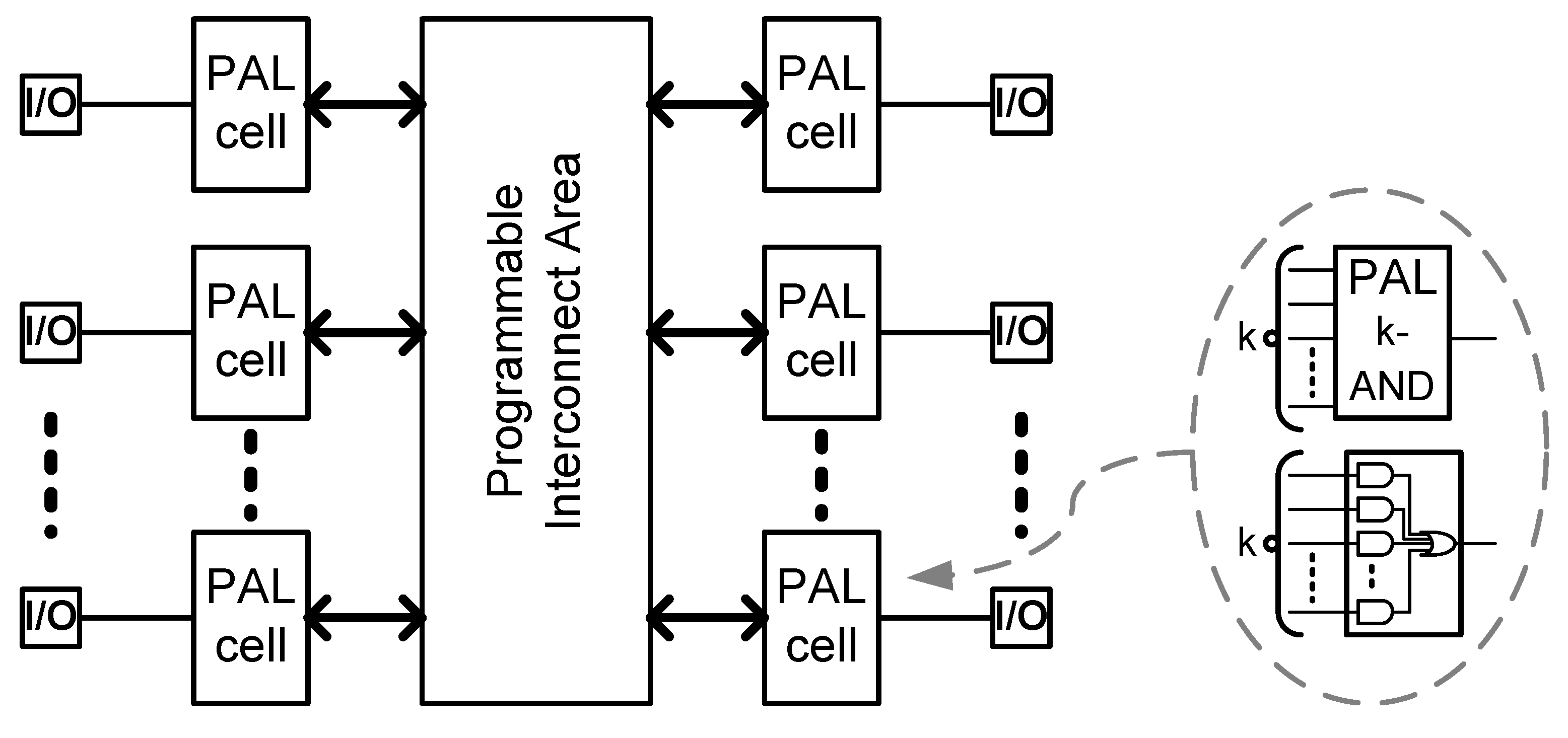
The root of CPLDs is related to PAL-based (programmable array logic) logic cells, which perform functions in the form of the sum of k-products. The structure of the CPLD is shown in
Figure 1. It should be mentioned that the first attempts to combine the best features of both circuits, FPGA and CPLD, appeared in the second half of the 1990s, when the idea of hyper-FPGA circuits was proposed [
9,
10]. The structure of the circuits includes LUT (look-up table) logic blocks associated with FPGA and PAL logic cells associated with CPLD. It turns out that the problem of logic synthesis dedicated to circuits including PAL-based cells remains to this day (it is still possible to limit the number of necessary resources in the implementation process) [
11,
12].
The synthesis process, which is implemented in well-known tools that support the process of design of digital circuits in CPLDs, begins with two-level minimization. The next stage of the synthesis process includes carrying out separate single output functions based on logic blocks that appear in the structure. This approach is logically connected with the inner architecture of CPLDs but introduces limitations into the process of multilevel circuit optimization. The reason for this problem lies in the method of logic synthesis in which the logic resources of a CPLD structure are not considered in the first stages. This synthesis strategy obviously has advantages such as easy solution transfer. However, the main drawback is inefficient use of terms included in the CPLD. Thus, it is necessary to search for synthesis methods that can enable effective implementation of a logic net in the form of the elements available in a given family of CPLDs. Only this approach is able to ensure efficient use of the resources in a programmable structure.
A series of valuable papers have presented various synthesis methods dedicated to optimization of the area of PAL structures. However, these studies were not implemented in commercial tools that support design of circuits and that mainly use the elements of multilevel optimization, synthesis of multivalue circuits combined with coding inputs and outputs, and the strategies of an appropriate partition of PAL matrixes based on decomposition [
13,
14,
15]. The essence of the synthesis is based on appropriate partition of the design and matching of separate extracts to the structure of logic blocks included in the CPLD. A classic synthesis method dedicated to PAL-based CPLD begins with two-level minimization, and it is usually a starting point in the process of technology-based optimization. Academic algorithms for technology-dependent decomposition oriented to CPLD lead to very efficient solutions [
16,
17], but it can be seen in these works that there is space to further improve the efficiency of the solutions obtained. However, the problem is connected to its substantial calculating complexity. The solution might be a logic function description in the form of BDD (binary decision diagram) [
18], or alternatively, the methods of multilevel optimization might improve the results.
The main goal of this paper is to present an original method for technology mapping of circuits in CPLD structures using a new form of the graphs. The original elements of the work are: application of optimization methods for output graphs described in [
19] to optimize the new form of graphs (graph of excitations and outputs) presented in the paper [
8] and the results of experiments (synthesis in commercial tools) showing the effectiveness of the implementation of the considered solutions in CPS.
The proposed logic synthesis method is dedicated to the most popular CPLDs, including PAL-based cells. The proposed method is a generalization of previously developed synthesis algorithms focused on CPLD devices [
20,
21]. In [
20], a concept was proposed that described multioutput combination circuits using an output graph. The theoretical basis for optimization of multilevel combinational circuits is based on the realization of shared implicants associated with each node of the graph of outputs with proof of the theorem on the selection of nodes of the graph of output and is shown in [
21]. These issues are presented in a summary form in
Section 2. After introducing the basic concepts, a simple example presents the essence of the basic concept of combinational circuit optimization using the graph of outputs.
Section 3 proposes a new method of optimization of a graph of outputs that reduces the resources used. The essence of the proposed optimization lies in matching the number of implicants to the number of terms contained in the PAL logic cells. This approach allows for better use of programmable structure resources and thus minimization of area in the target circuit. The idea of a technology mapping method for combinational circuits was extended to sequential circuits.
Section 4 presents the modification of a graph of outputs dedicated to synthesis of sequential circuits and is presented as a new form of a graph of outputs, the so-called graph of excitations and outputs, that describes the process of mapping of sequential circuits in CPLD. The proposed method of describing a multilevel circuit using the graph of excitations and outputs is universal. This approach forms the basis of a multilevel circuit optimization method in which its combination and sequential parts are optimized at the same time. This type of approach creates the possibility of further minimizing the area of the entire circuit.
The rest of the paper is organized as follows.
Section 2 contains the description of graph of outputs for combinational circuits.
Section 3 contains the methods for optimizing this graph.
Section 4 contains the description of the graph of excitations and outputs for sequential circuits.
Section 5 contains the results of the experiments.
Section 6 contains the conclusions.
2. Graph of Outputs in the Process of Synthesis of Combinational Circuits
A characteristic feature of PAL-based cells is that they enable logic functions to be carried out in the form of the sum of terms [
22]. The number of terms included in the PAL-based block is limited and is represented by the parameter
k. The value of the parameter
k is usually low. However, the CPLDs contain mechanisms that are flexible in terms of the choice of terms attached to the OR gate (hardware expanders). The process of carrying out a multioutput function in CPLDs consists of two stages. The first stage carries out minimization of a multioutput function that results in the set of implicants of separate functions belonging to a multioutput function. The second stage is based on mapping of functions in PAL-based cells including a given number of terms. The problem of minimization of a multioutput function is solved [
23]. A series of algorithms offers the ability to obtain excellent synthesis results. The problem of technology mapping is much more complicated. The original mapping methods (in the literature, known as the classical approach) did not co-share PAL-based blocks between logic structures associated with separate functions included in a multioutput function [
22]. This solution is inefficient with respect to the number of PAL-based blocks. Thus, it was necessary to create techniques to use this co-sharing. One of the solutions known from literature is the use of the graph of outputs Go < Y, U> for the mapping of combinational circuits [
17,
21].
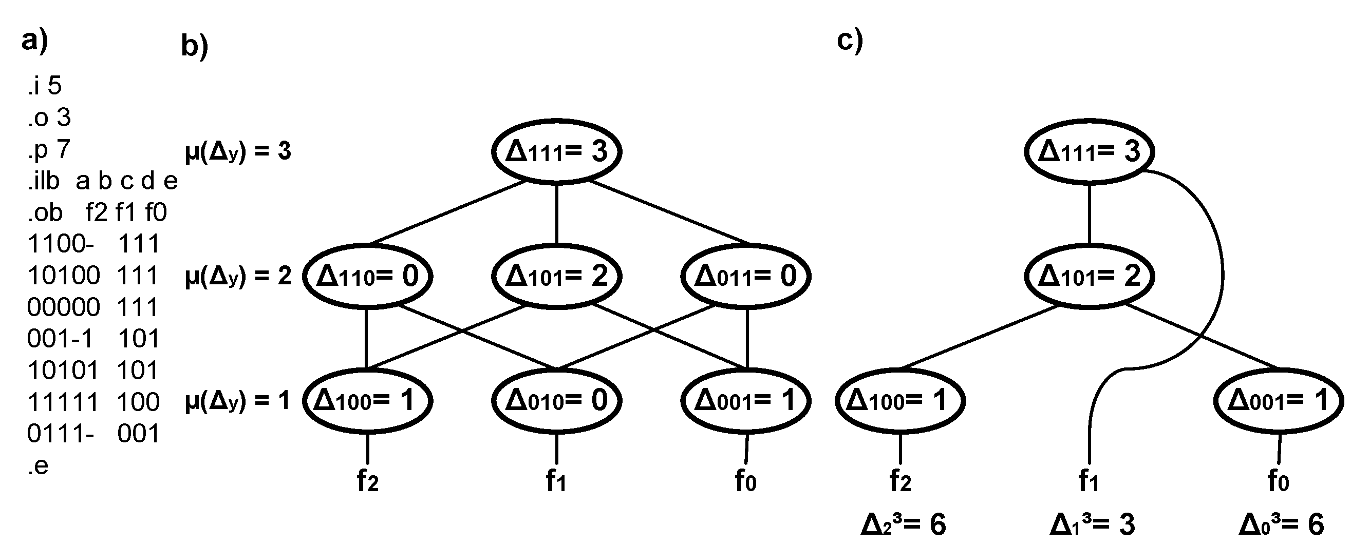
The nodes of a graph of outputs correspond to separate values of an output vector y. The vector represents values of separate functions belonging to a multioutput function. Parameter Δy is ascribed to each node and determines the number of implicants for which the same output vector y occurs. Number 1 in the vector y is a row of a node associated with a given vector μ(Δy). For example, if Δ101, then μ(Δy) = 2. The graph of outputs was arranged in a laminar way such that the nodes in a given level are in the same row. Separate levels were arranged in an ascending order, which depends on μ(Δy), such that the ‘lowest level’ corresponds to μ(Δy) = 1. Separate nodes placed on the next levels are combined with edges. Two nodes, described as Δys and Δyr, respectively, are combined with the edge if the Hamming distance between ys and yr is 1. The nodes for which μ(Δy) = 1 are only associated with a single i-function belonging to m–multioutput function, and thus, parameter Δim might be ascribed to them. The value of Δim is the sum of parameters Δy included in the nodes placed on paths that lead from the analyzed node in the first row (μ(Δy) = 1) to the node placed on the highest row.
It should be mentioned that a graph of outputs might be reduced by removing the nodes for which Δ
y =
0. A multioutput function, the graph of outputs, and a reduced graph of outputs are shown in
Figure 2. Analysis of the graph of
Figure 2c shows that, for example, Δ
23 = Δ
100 + Δ
101 + Δ
111 = 1 + 2 + 3 = 6. A formal description of the graph can be found in previous works [
21].
Based on the separate parameters Δ
im, the number of necessary PAL-based blocks (
δf) needed to carry out each function can be determined separately (1):
where H(x) = 1 when x ≥ 0 and H(x) = 0 when x < 0.
Let us consider a diagram from
Figure 2c. Assuming that
k = 3, the number of necessary PAL-based blocks needed to carry out a separate function is seven.
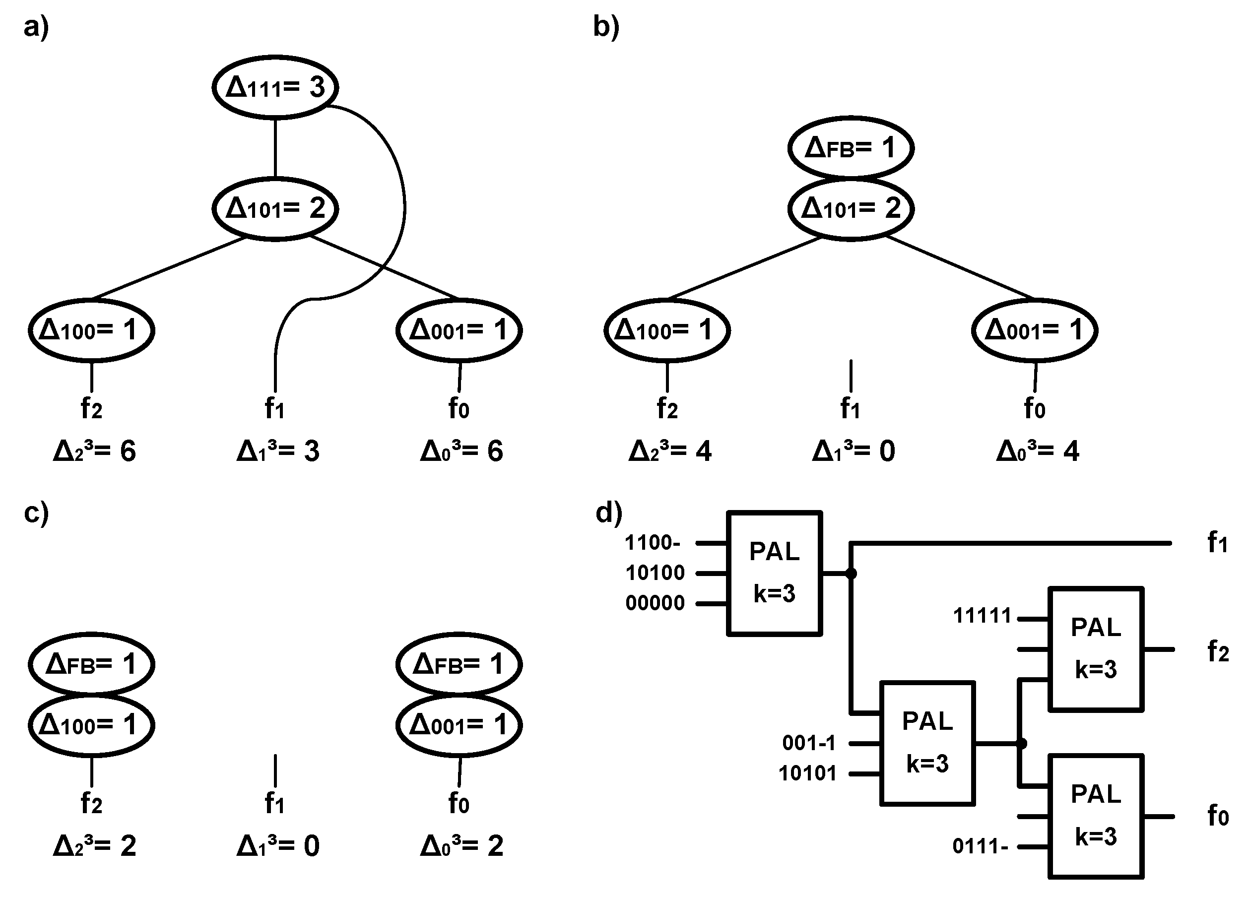
Technology mapping of a multioutput function considers the sharing of PAL-based blocks between separate logic structures associated with the functions included in a multioutput function. This process is applied to the graphs of outputs by replacing chosen nodes with the nodes representing feedback [
21]. The essence of this approach is explained in the following example.
Example:
Let us consider the function carried out on PAL-based blocks
k = 3, as presented in
Figure 2. The analysis of the graph from
Figure 3a starts from the node in the highest row for which Δ
111 =
3. Because the implicants associated with this node, correspond to all multioutput functions, they can be carried out in a separate block shared for all three functions. This node is removed from the graph. Whereas, the node that represents a feedback is added to the nodes to which were led the edges from the removed node. The value of the cofactor Δ
FB is 1 because the set of implicants from a shared block is replaced with a single line that leads to the structure associated with the nodes in lower rows. The Δ
FB represents the use of one term in the PAL logic block that is necessary to feed the signal from the CPLD output to the next PAL-type logic block. The multi-input implicant, used in one-bit feedback from the output of one block to the input of another, can be used to create a multilevel network logic block PAL.
The values of the cofactors Δ
im are modified. As a result, the graph presented in
Figure 3b is created. In the subsequent stage, the node in the second row for
y =
101 is analyzed, and it is shown in
Figure 3b. Carrying out the implicants associated with this node in a shared block for the functions f0 and f2 results in modification of the graph to the form shown in
Figure 3c. Because this graph has no nodes common for several functions, the structures associated with the functions f0 and f2 are carried out separately. Finally, a logic structure that consists of 4 PAL-based blocks was obtained and is presented in
Figure 3d. It can be seen that technology mapping considers sharing of PAL-based blocks using a graph of outputs. As a result, the obtained structure was reduced by three blocks compared with the basic number of blocks (1).
The most accurate description of an algorithm that carries out a multioutput function using a graph of outputs and a mathematical description can be found in previous studies [
17,
21].
3. Optimization of the Mapping Process—Modification of a Graph of Outputs
It is possible to optimize the process of technology mapping of combinational circuits in CPLDs. The essence of optimization is based on better usage of the available resources of PAL-based blocks that are associated with separate nodes of the graph of outputs. The aim of optimization is development of unused terms, which is possible by modifying the set of implicants associated with a given node of the graph of outputs. Let us assume that the node of a graph of outputs is associated with four implicants of the function
y (Δ
y =
4). Let us also presume that it must be mapped in PAL-based blocks
k = 3. Thus, the structure shown in
Figure 4 is obtained.
For this case, shown in
Figure 4, it is necessary to use two PAL-based blocks, but the terms of one of them are not fully used. The structure contains a single unused term that can be developed by modifying other implicants. A highly advantageous solution is to eliminate one of the implicants (Δ
y =
3), which might result in reducing one block of this structure. An excess implicant is one whose removal results in reducing the structure.
To conduct the process of optimization, it is necessary to describe separate nodes of a graph of outputs using an additional set of parameters. Let y be the number of excessive node’s implicants marked as ay and let Ly be the number of unused terms of a logic structure associated with this node. In addition, the number of feedback items, which originate from the structures associated with the nodes of higher rows, are marked as Ny. The process of optimization is passed on ‘carrying’ implicants between nodes in a manner designed to reduce the number of PAL-based blocks. Thus, it is necessary to analyze an output vector of an implicant. Separate output vectors were placed next to the appropriate nodes.
We can distinguish two basic techniques of relocating implicants in a graph of outputs that are the effect of either merging or splitting an output vector.
A merging method is based on an OR function for bits of output vectors of the implicants that underwent merging. As a result, we obtain the vector associated with the node in the higher row compared with the rows of vectors that underwent merging. The implicants that underwent merging are removed from the graphs. The implicant that is the result of merging is placed next to an appropriate node in a graph of outputs. The process of merging might involve only those implicants that have accurate input components, i.e., the same or accurate occurrences of the state ‘-’ at given positions. Merging leads to the relocation of implicants towards the nodes in higher rows.
The method of splitting is based on the partition of an output vector into several output vectors. After the OR operation, we obtain a vector before the partition. The implicant that underwent splitting is deleted from a graph of outputs. The implicants that are the result of splitting are placed next to the appropriate nodes in the graph. The implicants obtained as the result of splitting have the same output vector as the implicant that underwent splitting. The splitting operation leads to relocation of implicants towards the nodes in lower rows.
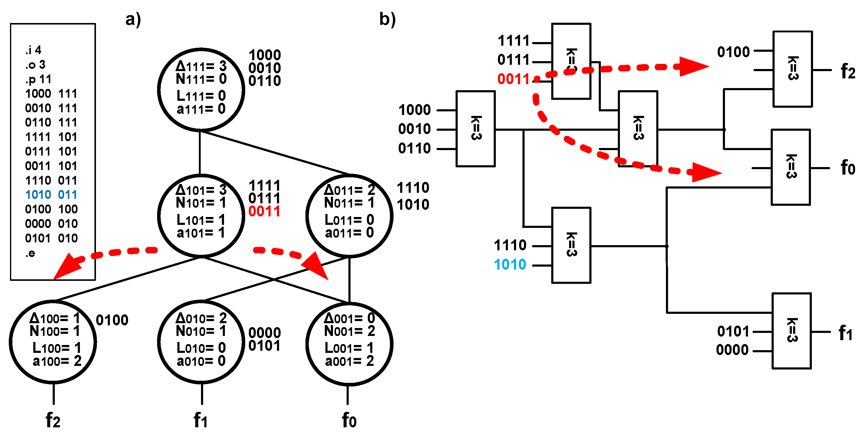
The idea of modifying a graph of outputs using the techniques of splitting and merging is presented in
Figure 5,
Figure 6 and
Figure 7. A multioutput function is described using a graph of outputs in the form shown in
Figure 5a (in addition, a description in the form of a pla file is placed). Technology mapping creates the structure that uses eight PAL-based blocks
k = 3 and is presented on
Figure 5b. The analysis of the graph from
Figure 5a starts with the node in the highest (the third) row. It is observed that cofactors describing the use of terms of a logic structure associated with this node are equal to zero (
a111 =
0,
L111 =
0). Thus, the terms of a PAL-based block are fully used, and no excessive implicants exist. In the subsequent stage, the nodes in the second row are analyzed. The node associated with the vector
y =
011 is described as
L011 =
1, meaning that that there is one unused term in the structure associated with this node. Because the nodes in lower rows are attached to an analyzed node and have the same input vector (1010), it is possible to carry out the process of merging. An excessive redundant implicant (
a010 =
1) exists for the node
y =
010, and its removal might lead to reduction of the structure associated with this node. The process of merging leads to a reduction in the number of PAL-based blocks.
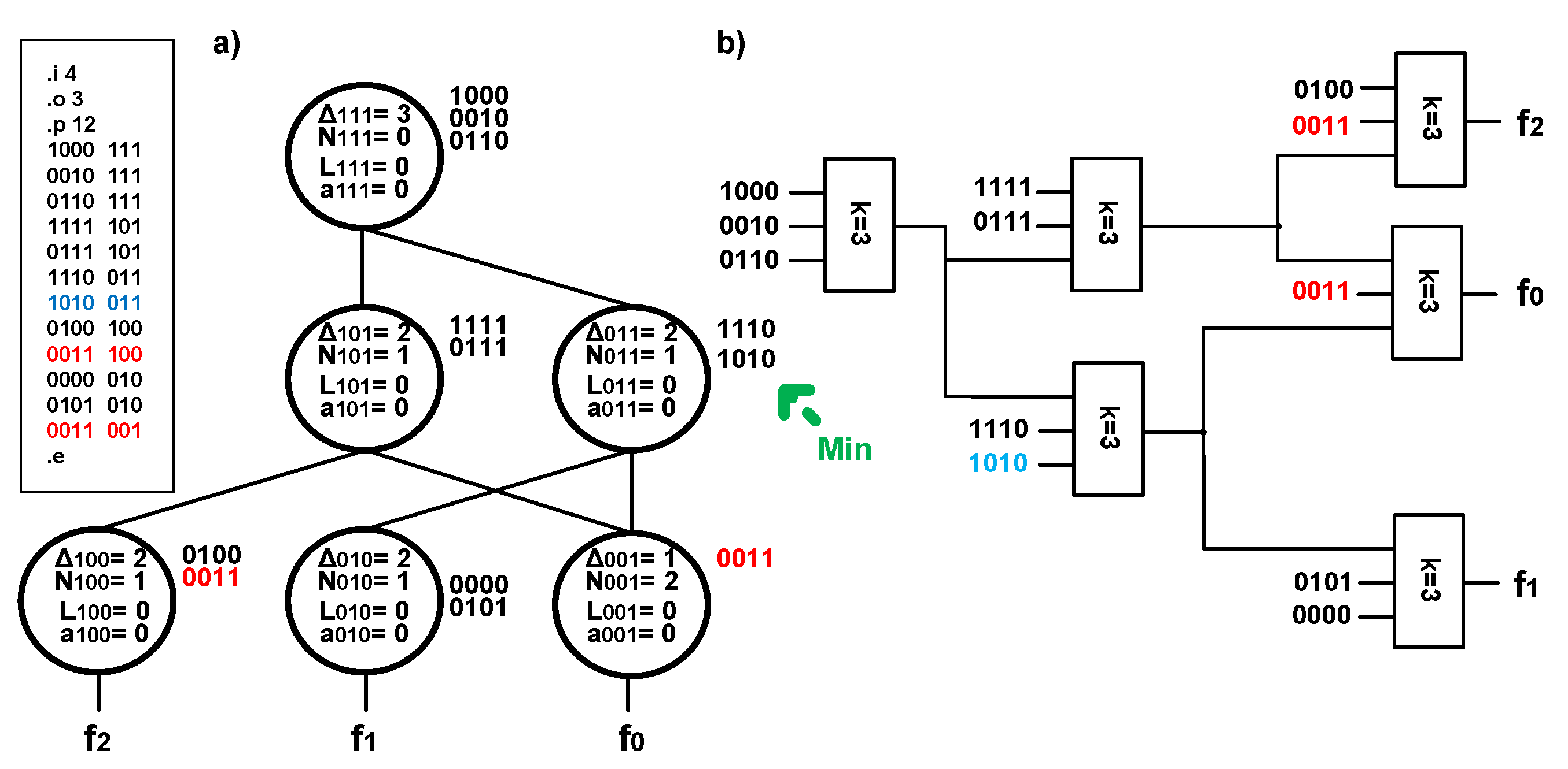
The process of merging modifies the graph of outputs, the description of pla, and the obtained logic structure, as shown in
Figure 6. As presented in
Figure 6b, the number of necessary PAL-based blocks was reduced to seven. Based on analysis of the node in the second row (
y =
101), it is associated with an excessive implicant (
a101 =
1).
Figure 6a shows that the nodes in the first row (
μ(Δ
y) =
1), which are attached to the analyzed node (
y =
100, y =
001), are also associated with logic structures that have unused terms. Thus, it is possible to apply the process of splitting that leads to reduction of a logic structure.
The process of splitting leads to modification of the graph of outputs, the description of pla, and the obtained logic structure, as shown in
Figure 7.
The process of splitting reduced one block in the obtained structure. All nodes of the graph presented in
Figure 7a are marked with the parameters
ay and
Ly, for which the value is zero. In this situation, the process of optimization should be completed. The optimization of mapping of three exemplary multioutput functions reduced the number of PAL-based blocks from eight (
Figure 5) to six (
Figure 7), a reduction of 25%. It is worth mentioning that for the node
y =
011, the implicants have such input vectors that might undergo merging. As a result of merging, two implicants 1110 and 1010, which have input vectors, can be replaced with a single implicant that has an input vector 1–10, and it influences the parameters associated with the analyzed node. Additional examples on the modification of graphs of outputs leading to optimization of technology mapping can be found in previous work [
19].
4. Graph of Excitations-Outputs in a Synthesis Process of Sequential Circuits
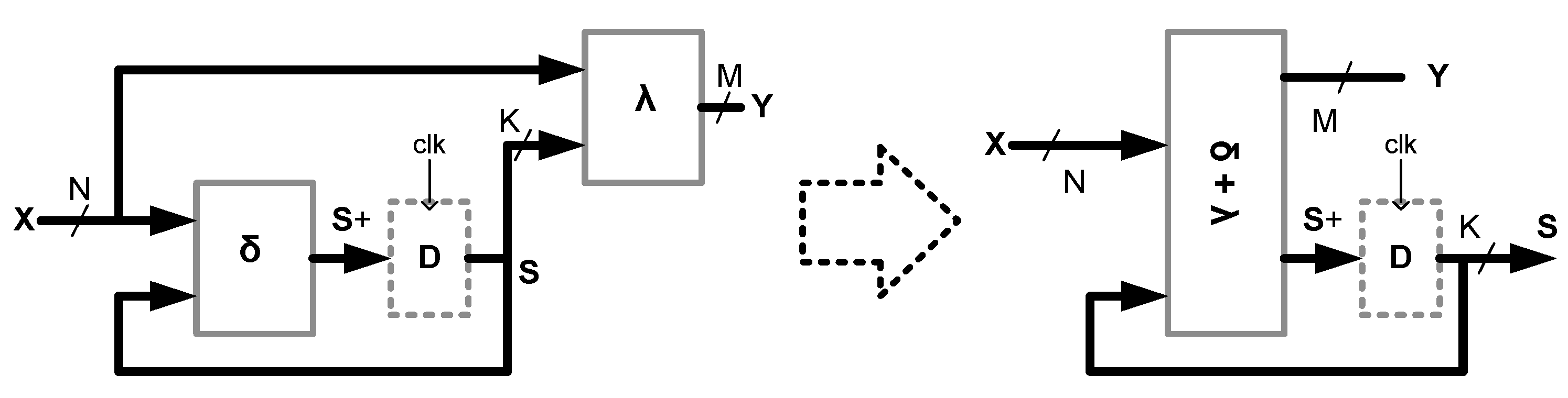
The key element of an FSM automaton is a memory block (D-FF) associated with the inner states of an automaton. In addition, FSM includes a combinational component that maps two multioutput functions. The first function is known as an excitation function δ: B
N+K→ B
K (where N is the number of FSM inputs, K is the number of state bits, B = {0,1}), and it is responsible for the process of changing states inside FSM. The second function is known as an output function λ: B
N+K→ B
M (where M is the number of FSM outputs), and it is responsible for creating an output FSM. It turns out that both multioutput functions can be presented at the same time by creating a new multioutput function δ+λ: B
N+K→ B
K+M, as shown in
Figure 8.
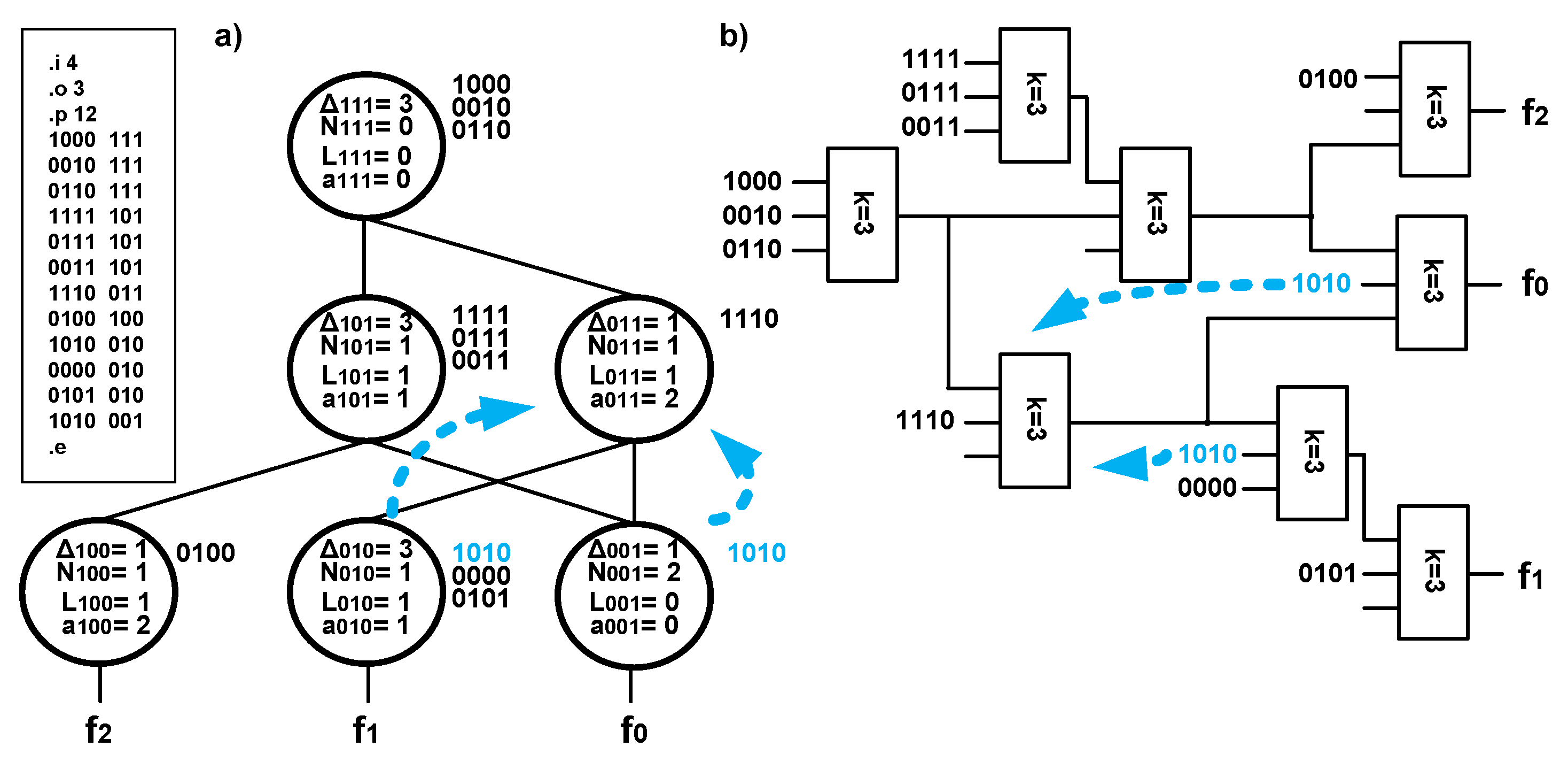
To describe a multioutput function δ + λ, a graph of outputs can be used that has been slightly changed. It is necessary to introduce two types of nodes: combinational nodes (denoted by circles on the graph) and sequential nodes (rectangles). Sequential nodes are placed in the paths associated with the excitation functions of particular D flip-flops. This newly created form of a graph is known as the graph of excitations and outputs [
8]. The description of a multioutput function in the form of a pla file and a graph of excitations and outputs is presented in
Figure 9a (without the nodes Δ
y =
0). Obviously, the description of a multioutput function δ + λ in this form requires new coding of the inner states in FSM.
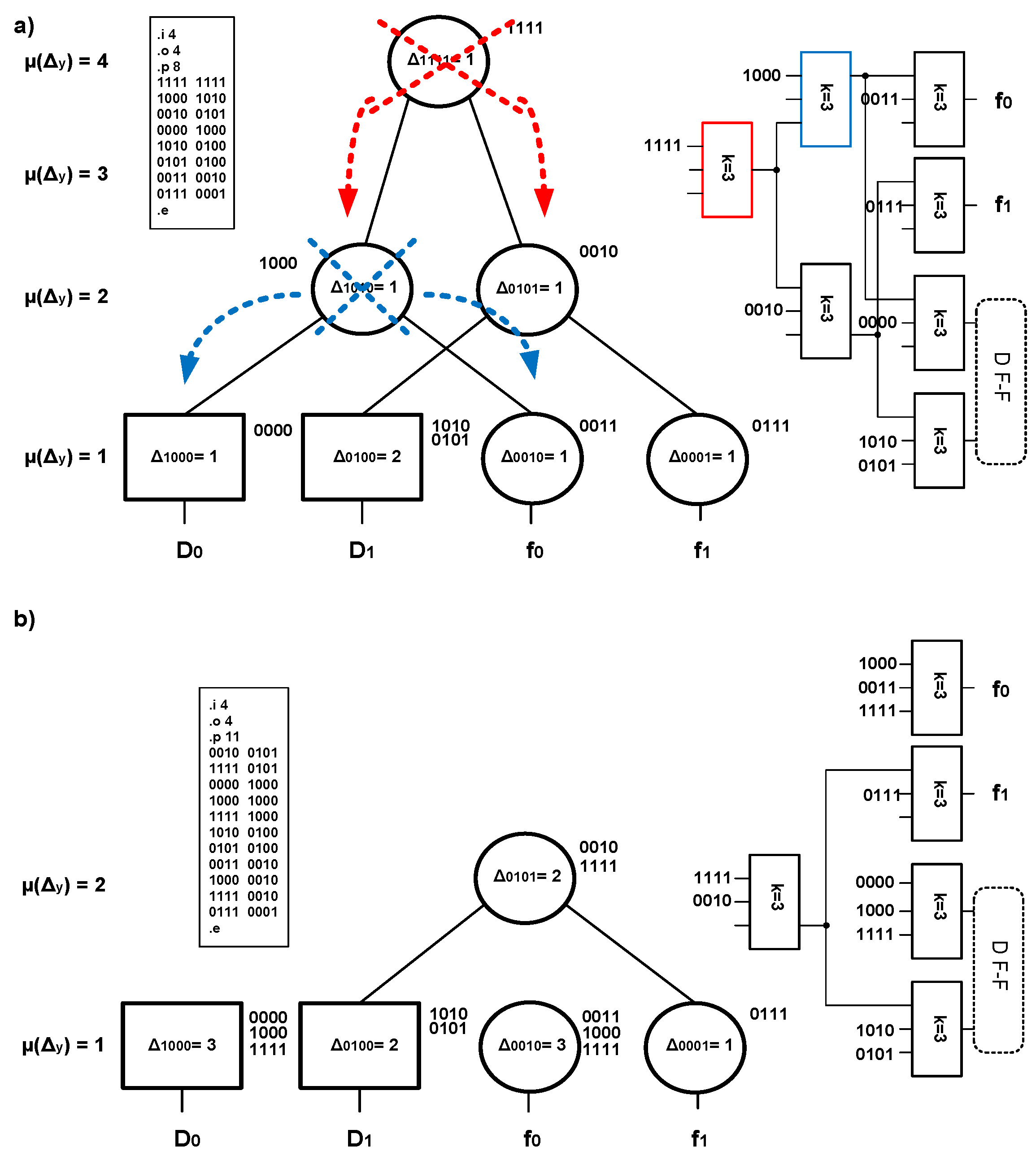
A graph of excitations and outputs might undergo the process of optimization using the methods described in
Section 3. As shown in
Figure 9, the original graph from
Figure 9a underwent optimization such that two nodes (
y =
1111, y =
1010) were subjected to the process of splitting of an output vector. This modification reduced the graph from
Figure 9a and the logic structure from
Figure 9b compared with the structure from
Figure 9a. In general, synthesis of FSM is widely analyzed in many scientific papers [
22,
24,
25,
26,
27]. It should be noted that the proposed optimization integrated with technology mapping might be an essential extension of a series of coding methods of states in FSM and could lead to limitations of the used logic resources of the given CPLDs or minimization of power consumption.
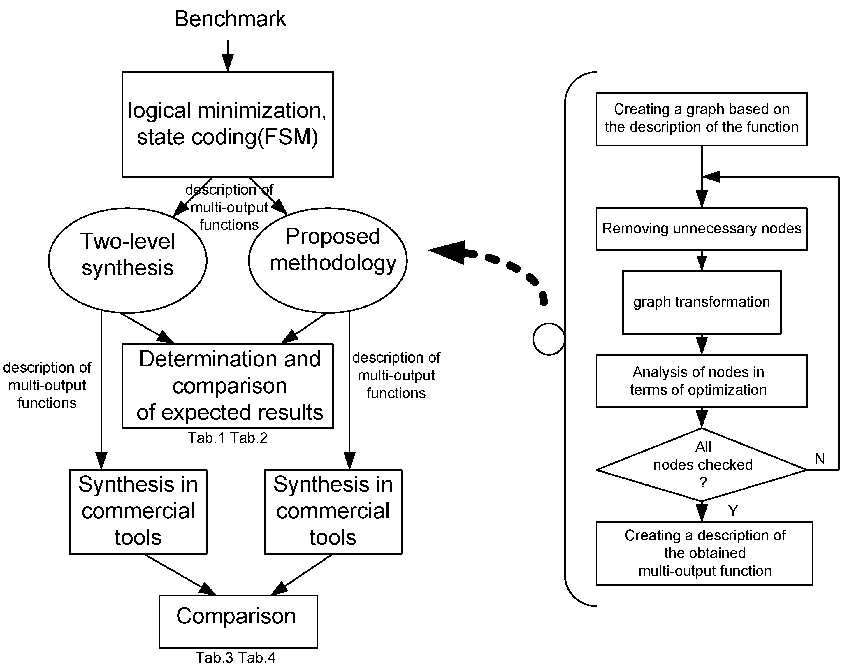
5. Experimental Results
A series of experiments were conducted to compare the efficiency of the method for technology mapping of circuits in CPLDs. We focused on both combinational and sequential circuits. The experiments were conducted on well-known benchmarks [
28]. The results of the comparison are illustrated in
Table 1,
Table 2,
Table 3 and
Table 4.
An appropriate research flowchart showing the essence of conducting experiments is shown in
Figure 10. In addition, this figure presents an outline of the graph analysis algorithm. Depending on the adopted strategy, the process of splitting or merging nodes may play a dominant role. This leads to the appropriate modification of the graph together with the possibility of removing the considered node. The last element of the algorithm is to create a description of the set of functions that can be further synthesized on commercial tools.
Table 1 includes the synthesis results of the chosen combinational circuits using two methods: the method without multilevel optimization (two-level synthesis) and the method using a graph of outputs in technology mapping (proposed approach). The table consists of three parts. The first part includes the features of a benchmark, i.e., its name (NAME), the number of inputs (IN), the number of outputs (OUT) and the number of product terms (p). The second part includes the results of logic synthesis without multilevel optimization. This method is based on two-level optimization and is described in a shortened form (two-level synthesis). The third part of the table includes the results of synthesis using the proposed method. Technology mapping is characterized by three parameters: the number of used PAL-based blocks, which includes five terms (Block), the number of logic levels in the longest path (Level), and the synthesis time (Time).
Analysis of the experimental results clearly indicates that the effect of multilevel optimization is minimization of the number of blocks required to process the benchmarks. In the set of 12 benchmarks, in eight cases (67%), the solution was obtained using a lower number of PAL-based blocks. In three cases (5xp1, b12, duke2), use of a graph of outputs in the process of technology mapping did not lead to a decrease in the number of used blocks. The total number of blocks, given in the last row in
Table 1, indicates that use of the proposed method reduced the number of blocks required to process all the benchmarks at 28% (((1082 − 781)/1082) × 100%)).
The expansion of the number of logic levels is an unfavorable effect of reducing the number of logic blocks. Unfortunately, multilevel optimization prolongs critical paths, which was observed in ten cases (83%). In the other two cases (alu2, b9), the same number of logic levels was obtained. Considering the total number of logic levels obtained for all analyzed benchmarks, the number is 56% higher (((52 − 33)/33) × 100%) in multilevel optimization than in the method based on two-level synthesis.
It is worth emphasizing that multilevel optimization does not prolong synthesis time. The total synthesis time for all analyzed benchmarks slightly differs at approximately 5%. It should also be mentioned that in the largest circuits, the method of multilevel optimization limited the number of logic blocks and was performed in a substantially shorter time than that using a classic attitude with two-level minimization.
A similar comparison was conducted for sequential circuits. A combinational FSM approach, including both a description of a transition block and an output block, underwent synthesis [
8]. An estimated method of coding inner states was assumed, and in cases where this was not possible, a natural binary code was used. In the process of multilevel optimization, a graph of excitations and outputs was used. The first portion of
Table 2 shows the column ‘s’ that includes the number of states of a sequential automaton. The remainder of
Table 2 is the same as
Table 1. The columns named ‘Block’ include the total numbers of PAL-based blocks needed to carry out an appropriate FSM without distinguishing between use of flip-flops or without them.
In the set of analyzed FSMs, we found six cases (50%) for which technology mapping uses a lower number of blocks. In five cases (dk17, ex2, ex3, ex4, mc), the use of the graphs of excitations and outputs in technology mapping increased the number of used blocks. The total numbers of blocks indicate that use of the proposed technology mapping method reduced the number of blocks needed to carry out all the automatons at 16%.
As in the case of combinational circuits, the expansion of the number of logic levels is a side effect of multilevel optimization. Thus, it is necessary to decrease the maximum clock frequency in FSM. Multilevel optimization means that FSM works slowly in eight cases (67%). In other cases, the same number of logic levels was obtained.
In the case of FSMs, multilevel optimization prolongs the synthesis time. In the case of the largest automatons (s822, s830), the synthesis time was slightly prolonged and was 4% and 10%, respectively.
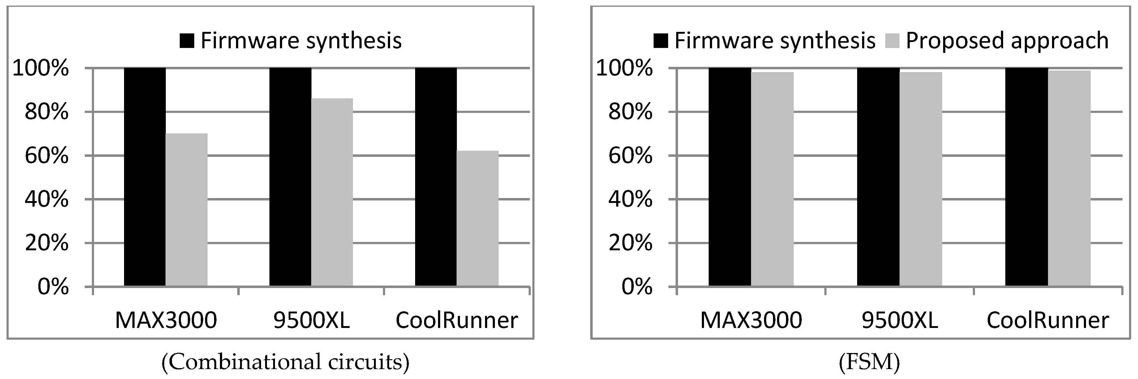
Similar experiments were conducted using Quartus and ISE tools. This time, synthesis was conducted using two methods. In the first case, synthesis was conducted in an appropriate system that supports a synthesis process and uses a description of a circuit in the form of VHDL. In the second case, a description of a structure in VHDL underwent synthesis using a commercial tool. VHDL was created in a prototype programmable tool that performs the multilevel optimization process presented in this paper. The process of optimization was carried out for PAL-based blocks, including five terms as basic logic blocks in commercial circuits that have the same number of terms. In addition, the CPLDs include various types of expanders that offer the possibility of further solutions in commercial tools. The experiments were conducted using the same set of benchmarks for three families of CPLDs: the MAX3000 [
29] family, Altera company, and circuits from families 9500Xl [
30] and CoolRunner II [
31] by Xilinx.
Table 3 includes the synthesis results of combinational circuits. Apart from the characteristic features of benchmarks, we present the numbers of macrocells used to construct the circuits (MC). The circuit from the Max300 family was given a usage percentage of MAX 3512 (%). The circuits by Xilinx were given the number of terms used to carry out separate benchmarks (Pt). The parameters included in
Table 3 were read out from the results of the reports after synthesis in Quartus and ISE.
While carrying out synthesis in Quartus, it was observed that an appropriate description of a circuit, which is the effect of a multilevel optimization, made the results better. Considering the use of macrocells, the result was better in seven cases (58%) compared with solutions in which synthesis was performed by an original description of a circuit in VHDL. In one case (rd73), initial multilevel optimization did not reduce the number of macrocells.
In the case of Xilinx devices, for the circuits from the 9500XL family, the proposed optimization method limited the number of macrocells in eight cases (67%), and the others (33%) showed a slight increase in the number of blocks. For CoolRunner II circuits, the initial multilevel optimization turned out to be advantageous in six cases (50%). In other cases, either the number of blocks was the same (3.3%) or it was increased (17%).
The same experiments were carried out for FSMs, and the results are illustrated in
Table 4.
In the case of FSMs, we observed smaller differences in CPLDs. For Quartus, in most cases, the number of blocks, i.e., as the effect of initial multilevel optimization, was not limited. In two cases (ex2, s1488), we observed a slight reduction in the number of macrocells. In the case of the ISE system, the differences were unnoticeable. In most cases, we observed the use of the same number of macrocells. The group of the analyzed FSM contains cases in which the number of macrocells was limited or increased.
Figure 11 presents a comparison of synthesis experiments carried out using commercial tools.
It was assumed that the results obtained in synthesis using commercial tools without an initial multilevel optimization act as a reference point, i.e., they correspond to the value 100% on the graph.
Analysis of the data presented in
Figure 11 indicates that initial multilevel optimization improved the synthesis results. The situation is the same for both combinational circuits and FSMs. It should be mentioned that the advantages for FSMs are rather limited (2%). However, it should also be emphasized that the methods of multilevel optimization could be more advantageous if the process of technology mapping was integrated with a commercial tool. Multilevel optimization carried out without a commercial tool is not able to fully use the potential of developed methods. The results included in
Table 1 and
Table 2 best illustrate this situation. The proposed method of multilevel optimization reduced a higher number of blocks in combinational circuits (28%) than in the case of sequential circuits (16%). It is clearly observed that in the case of synthesis in FSMs, their potential is more limited than in the case of technology mapping using commercial tools. In the second case, the number of macrocells was reduced at 2%.
7. Future Work
The experimental results clearly indicate that the proposed method of technology mapping is efficient in the way that it uses the area of a programmable structure. A side effect is the expansion of the number of logic levels, which might have a disadvantageous influence on the dynamic features of the solutions. Based on the presented results, situations exist in which the method of technology mapping produces worse results than two-level synthesis. However, no barrier exists to choosing a better solution after carrying out the synthesis using two methods. It is also worth considering that the calculation complexity of the proposed algorithms is comparable to that of the method of technology mapping based on two-level minimization.
The above conclusions encourage further work, but also show the weaknesses of our method. Unfortunately, it does not always lead to better solutions, which would require synthesis by various methods, and after analyzing the result, choosing a better solution. This type of approach is sometimes used, but for the synthesis of complex circuits it is quite tedious. Another disadvantage of the proposed circuit implementation is the higher number of logic levels, which often leads to a slight deterioration of the dynamic properties of the solutions obtained in comparison to alternative methods. The above disadvantages and limitations of the proposed method indicate the direction of further work.
First, we intend to develop a criterion that will allow you to decide on the method of technology mapping of the analyzed functions at the initial stage of the synthesis. It seems that this is possible, because knowing the result of two-level minimization can predict which of the technology mapping methods will lead to more efficient mapping.
The second direction of work will be the search for technology mappings in which minimizing the area goes hand in hand with minimizing the number of logical levels. One idea that could lead to further optimization is the idea of using three-state output buffers in the process of technology mapping. Such buffers are commonly found in the output cells of programmable devices and are very often unused. The concept of using three-state buffers has proven itself in the implementation of combinational circuits implemented in older programmable devices families. It is difficult to say whether it will work out what needs to be checked, also analyzing the issues of power consumption of the solutions obtained.
All planned works are related to the optimization of CPS computing and control systems implemented in programmable devices. They concern the lowest layer of CPS, i.e., the physical layer. In addition, we are considering focusing our research on specific CPS applications that could be effectively implemented in programmable devices.
These conclusions show that an extremely important element of CPS synthesis is appropriate technological mapping focused on the system implementing the function of the CPS physical layer.


