Article

Active Feedback-Driven Defect-Band Steering in Phononic Crystals with Piezoelectric Defects: A Mathematical Approach

Department of Mechanical, Robotics, and Energy Engineering, Dongguk University, Seoul 04620, Republic of Korea
Mathematics 2025, 13(13), 2126; https://doi.org/10.3390/math13132126
Submission received: 21 May 2025 / Revised: 21 June 2025 / Accepted: 27 June 2025 / Published: 29 June 2025
(This article belongs to the Section E2: Control Theory and Mechanics)

Abstract

Defective phononic crystals (PnCs) have garnered significant attention for their ability to localize and amplify elastic wave energy within defect sites or to perform narrowband filtering at defect-band frequencies. The necessity for continuously tunable defect characteristics is driven by the variable excitation frequencies encountered in rotating machinery. Conventional tuning methodologies, including synthetic negative capacitors or inductors integrated with piezoelectric defects, are constrained to fixed, offline, and incremental adjustments. To address these limitations, the present study proposes an active feedback approach that facilitates online, wide-range steering of defect bands in a one-dimensional PnC. Each defect is equipped with a pair of piezoelectric sensors and actuators, governed by three independently tunable feedback gains: displacement, velocity, and acceleration. Real-time sensor signals are transmitted to a multivariable proportional controller, which dynamically modulates local electroelastic stiffness via the actuators. This results in continuous defect-band frequency shifts across the entire band gap, along with on-demand sensitivity modulation. The analytical model that incorporates these feedback gains has been demonstrated to achieve a level of agreement with COMSOL benchmarks that exceeds 99%, while concurrently reducing computation time from hours to seconds. Displacement- and acceleration-controlled gains yield predictable, monotonic up- or down-shifts in defect-band frequency, whereas the velocity-controlled gain permits sensitivity adjustment without frequency drifts. Furthermore, the combined-gain operation enables the concurrent tuning of both the center frequency and the filtering sensitivity, thereby facilitating an instantaneous remote reconfiguration of bandpass filters. This framework establishes a new class of agile, adaptive ultrasonic devices with applications in ultrasonic imaging, structural health monitoring, and prognostics and health management.
MSC:
34A25; 81U15; 82C21

1. Introduction

Extensive investigations in recent decades have demonstrated that phononic crystals (PnCs), consisting of periodically arranged unit cells, can manipulate elastic waves in unconventional ways because of their periodic nature [1,2,3]. This finding has broadened the scope of potential engineering applications. One such method involves using defective PnCs to localize and amplify wave energy within designated regions [4,5]. Conversely, conventional defect-free PnCs exhibit phononic band gaps that impede wave propagation due to their strict periodicity and the resulting constructive and destructive interference patterns [6,7,8].
Defects are introduced into defect-free PnCs by substituting a unit cell with an alternative structure that differs in geometry or material composition [9,10]. The structural configuration resulting from this substitution is designated as a defective PnC. Defective PnCs have been shown to generate one or more defect bands inside phononic band gaps [11,12,13]. It has been previously established that evanescent waves, an inherent property of the band gaps, virtually induce fixed boundary conditions within defective PnCs [14]. This phenomenon leads to resonant motion at each defect-band frequency. This behavior, commonly referred to as a defect mode, results in a pronounced wave localization in and around the defect [15,16,17].
This field is currently undergoing significant evolution, transitioning from initial theoretical explorations and parametric studies to the development of prototypes that leverage the extraordinary properties of PnCs. In recent years, a concerted effort has been made to integrate intelligent materials into PnC designs [18,19,20,21]. This integration signifies a pivotal transition in the trajectory of research, propelling it toward commercialization. These intelligent materials, which manifest mechanical stresses and strains in reaction to external stimuli, can achieve the multiple functionalities of defective PnCs. These materials can be utilized in two primary structural capacities: either as defects or as attachments to defects or unit cells. The present study places particular emphasis on piezoelectric materials, which have garnered significant interest. The exploitation of defect-mode-induced energy localization at specific frequencies in engineering applications includes bandpass filters [22] and ultrasonic receivers [23].
Despite the encouraging outcomes, the bandpass filtering and energy amplification capabilities of defective PnCs are inherently constrained by their limited effective frequency ranges. These systems function optimally only when the uncontrolled excitation frequency matches the prescribed defect-band frequency. Unfortunately, the unchangeable defect-relevant characteristics of fabricated PnCs limit their practical applicability in engineering scenarios where excitation frequencies vary, such as in rotating machinery [24,25]. From a mechanical engineering perspective, one potential solution is to design reconfigurable defective PnCs using an advanced kinematic approach [26,27]. Alternatively, integrating defective PnCs with Winkler foundations enables the external tuning of the effective stiffness of both the unit cell and the defect [28]. However, these strategies inherently introduce additional design complexity or require extremely high manufacturing precision.
Recent investigations have increasingly focused on leveraging the multiphysics interactions of intelligent materials to modify defect-related characteristics through external stimuli without altering the underlying mechanical configuration. For instance, temperature-responsive materials have been integrated into defective PnCs to tune stiffness as a function of temperature [29,30,31], resulting in an approximate 5% shift in the defect band. However, the slow response times of these materials have limited their practical application. Alternatively, the application of magnetic fields to magnetostrictive rods or electric fields to piezoelectric materials and dielectric elastomer layers has been investigated [32,33,34,35]. While these approaches facilitate near-real-time adjustments of defect-band frequencies, the variations are modest, typically ranging from a small percentage to a few tenths of a percentage. This observation underscores the necessity for further advancements to substantially broaden the tunable frequency range.
To address this challenge, two approaches have been recently put forth that utilize electric circuits connected to piezoelectric materials. The initial approach entails the implementation of a synthetic negative capacitor, which abruptly alters the effective stiffness of the piezoelectric materials [36]. This method enables the manipulation of the pre-existing band structures in the absence of electric circuits across the entire band gap. The second approach entails the use of an inductor, where the interplay between the piezoelectric capacitor and an externally connected inductor induces electrical resonance, thereby generating a new defect band [37]. The defect band can be manipulated throughout the band gap by adjusting the inductance value. While circuit-based methods demonstrate the capacity to tune pre-designed PnCs over a substantial frequency range, their reliance on the manual manipulation of circuit parameters, such as potentiometer adjustments or inductor substitutions, restricts their applicability for online or on-demand control when targeting specific frequencies. Consequently, there is an imperative for a methodology that (i) enables remote tuning of the defect-band frequency and (ii) can be adjusted over a wide frequency range.
Therefore, referring to Refs. [38,39,40], this study proposes a methodology that employs active feedback control to dynamically manipulate the energy-localized behavior of defective PnCs in longitudinal waves. The proposed approach is demonstrated using an electrically tunable bandpass filter. To strengthen the fundamental underpinnings of the feedback control approach, a transfer matrix-based analytical model is formulated to capture variations in band structure and transmittance analyses. The system includes bimorph piezoelectric devices strategically positioned on the bottom and top surfaces of the defect. The piezoelectric materials in proximity to the defect function as sensors, while those in more distant regions serve as actuators. The voltage generated by the sensors is amplified using a controller and applied directly to the actuators. This amplification factor, designated as the gain, is instrumental in regulating the degree of electroelastic coupling among the integrated piezoelectric devices, thereby enabling online adjustment of defect bands across entire band gaps. The desirable result is illustrated schematically in Figure 1.
To the best of the author’s knowledge, this work is the first to employ active feedback control for the continuous, wide-range tuning of defect bands in one-dimensional PnCs. Consequently, the absence of feedback-based tuning algorithms renders direct numerical comparisons unfeasible. The simple linear feedback law employed in this study is selected to elucidate the fundamental feasibility of completely remote, on-demand band-tuning. It is anticipated that subsequent studies will build upon this framework to incorporate more advanced control schemes, such as adaptive or optimal controllers. At that point, systematic performance comparisons will become possible.
The ensuing sections are structured as such. In Section 2, the targeted electrically tunable bandpass filters are introduced. The construction of these filters involves a one-dimensional defective PnC, with active feedback control utilized. Section 3 unfolds the proposed analytical model, integrating gains from active feedback control to effectively predict the outcomes in terms of transfer matrix and S-parameter methods. In Section 4, numerical case studies are presented that demonstrate how individual (displacement, velocity, acceleration) and combined feedback gains shift the defect-band frequency and transmittance. These studies illustrate continuous electrical tunability. As delineated in Section 5, the primary findings are summarized, and prospective avenues for future research are proposed.

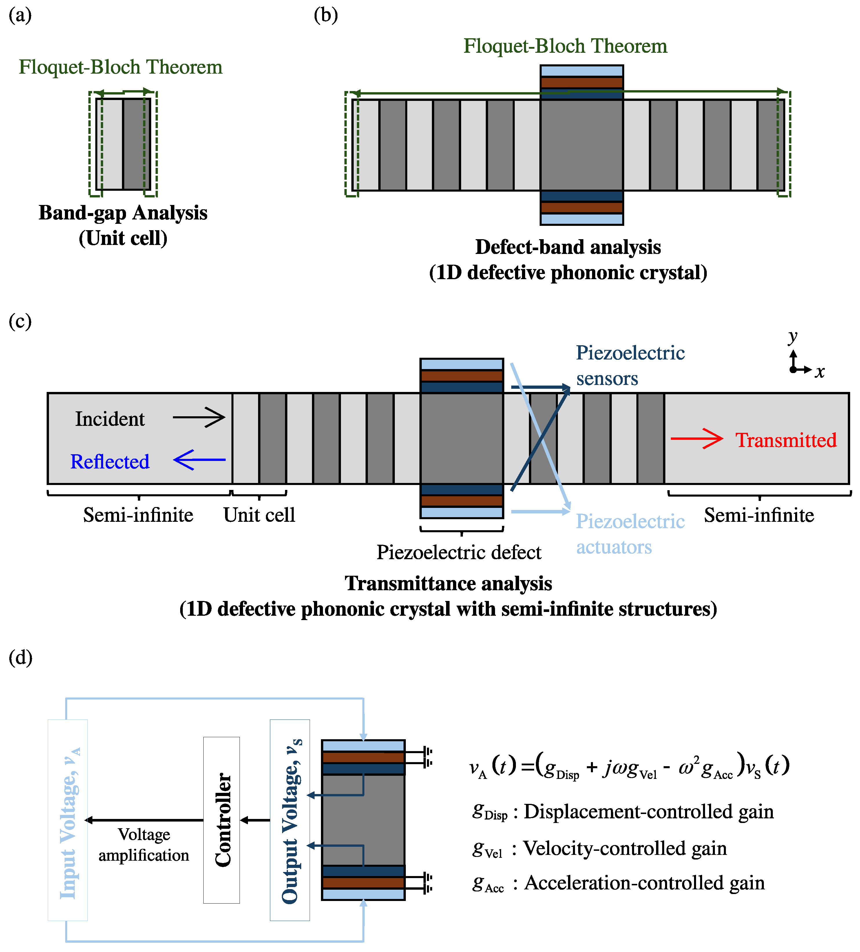
2. Target System Description

As shown in Figure 2, the 1D PnC is constructed by repeating N unit cells, with each unit cell comprising two distinct materials. The alteration of the length of the dark gray structure at the D-th unit cell results in the imposition of a defect, and bimorph piezoelectric devices are fully mounted on its top and bottom areas. Each piezoelectric device under scrutiny is composed of two piezoelectric layers, depicted in light and dark blue, bonded on the upper and lower sides of a thin substrate colored brown. The defect region under investigation, thus, contains seven substructures, each consisting of three materials, collectively referred to as the piezoelectric defect. Two substrates and four piezoelectric layers exhibit, respectively, identical material properties and geometric dimensions, thereby ensuring that these substructures are arranged symmetrically concerning the xy-plane. The piezoelectric layers are composed of piezoceramics, while the remaining elements are metallic.
The dispersion analysis is an investigative method that focuses on understanding band gaps, defect bands, and defect-mode shapes. This analysis is constrained to unit cells and defective PnCs and utilizes periodic boundary conditions, as shown in Figure 2a,b. The transmittance analysis entails the propagation of mechanical waves from the front region (left side) into the defective PnC and through to its rear region (right side). As depicted in Figure 2c, additional configurations include semi-infinite light gray structures. As a result, incident waves and reflected waves are superimposed in the front region, while transmitted waves are present in the rear region. In comparison, finite-length structures pose significant challenges due to boundary conditions that induce additional reflections and resonant motions throughout the entire structure.
The geometric dimensions are specified by the following symbols: ‘l’ for length, ‘h’ for height, and ‘w’ for width, while the cross-sectional area in the yz-plane is denoted by ‘A.’ The material properties are characterized by the mass density (‘ ρ ’) and Young’s modulus (‘Y’). For piezoelectric layers, the piezoelectric coupling coefficient in the 31-mode is indicated by ‘ e PP ,’ and the dielectric constant measured under constant strain is denoted by ‘ ε PP S .’ The corresponding constitutive equations are as follows:
(1a) T m = Y m S m , (1b) T PP = Y PP S PP e PP E PP , D PP = e PP S PP + ε PP S E PP ,
where the subscript ‘m’ is constrained to set {UL, UD, D, PS, SL, SR}. Each string corresponds sequentially to different structural elements, including the light gray and dark gray components within the unit cells, the defect, the substrates used in bimorph piezoelectric devices, and the semi-infinite structures positioned to the left and right. Additionally, the subscript ‘PP’ denotes the piezoelectric layers. Moreover, the subscripts ‘U,’ ‘PD,’ and ‘PnC’ refer to attributes pertinent to the unit cell, the piezoelectric defect, and the overall defective PnC, respectively. ‘T’ and ‘S’ denote the x-axial normal stress and strain, respectively, while ‘E’ and ‘D’ represent the z-axial electric field and electric displacement, respectively. Note that these quantities in Equation (1a,b) are scalars. Although constitutive equations typically take a matrix form, this study simplifies them into three scalar equations by neglecting lateral and shear deformations [41]. This approach is particularly well-suited for investigating longitudinal waves in a relatively low-frequency regime (tens of kHz). The 31-mode in piezoelectric coupling is defined as the piezoelectric material’s inherent characteristics. In this case, the application of an electrical field through the thickness (3-direction) produces a longitudinal strain in the in-plane (1-direction) axis, or vice versa. The coefficient is defined as the quantitative value that represents the interactions between the mechanical and electrical domains.
The present focus is directed toward piezoelectric layers within the defect, as illustrated in Figure 2d. It is hypothesized that the electric fields in these piezoelectric materials are induced exclusively along the z-axis. Consequently, the x-axial normal strain generates the z-axial electric field (from a piezoelectric sensor perspective), or, conversely, the z-axial electric field produces the x-axial normal strain (from a piezoelectric actuator perspective). Furthermore, it is assumed that the thickness of the piezoelectric layers is sufficiently small to ensure a uniform electric field across the entire area. Note that a common rule of thumb is that the thickness of the layer should not exceed approximately 10% of the smallest in-plane dimension. In the case of fields exhibiting a lower ratio, the fringing fields located at the edges contribute an insignificant amount, typically less than a small percentage, to the total field. Consequently, the through-thickness field can be regarded as uniform. Of the four piezoelectric layers, two of them, which are adjacent to the defect, function as sensors (colored dark blue). When these sensors are electrically connected in parallel under open-circuit conditions, they produce an output voltage, denoted as ‘ v S ( t ) .’ This voltage is fed to an external controller, which amplifies it by a factor of ( g Disp + i ω g Vel ω 2 g Acc ), resulting in an amplified voltage, ‘ v A ( t ) = ( g Disp + i ω g Vel ω 2 g Acc ) v S ( t ) .’ The amplified voltage is then supplied to the remaining piezoelectric layers (colored light blue), which are connected in parallel and function as actuators. In this configuration, the gains ‘ g Disp ,’ ‘ g Vel ,’ and ‘ g Acc ’ control the displacement, velocity, and acceleration of the piezoelectric actuators, respectively.
Active feedback control is a system that utilizes real-time sensing and actuation. Piezoelectric sensors embedded in defective PnCs measure the local wavefield (e.g., strain or velocity). These signals are then converted into voltage and subsequently fed into a digital/analog controller that implements a proportional control law. The controller functions to direct the additional piezoelectric actuators to either inject or absorb energy. This continuous loop enables on-demand, software-driven tuning of the defect-band frequency during operation. Conversely, passive control (or passive shunting) utilizes a fixed analog network—–such as an inductor–capacitor–resistor circuit or synthetic negative capacitance—attached to the piezoelectric layers. The dynamic stiffness of the system is determined at the design stage by the selection of circuit components, offering simplicity and independence from external power sources, with the exception of pre-set tuning points. Mathematically, a passive shunt can be conceptualized as a particular instance of zero-order constant feedback. In contrast, active control expands this concept to encompass frequency- or time-varying feedback gains.

3. Analytical Modeling with Active Feedback Control

3.1. Governing Equations and Corresponding Solutions

This subsection commences with an examination of the piezoelectric defect. In accordance with classical rod theory, the displacement field across any cross-section parallel to the yz-plane is assumed to be uniform. Consequently, the x-axial displacement field is expressed as ‘ u PD ( x PD , t ) ,’ where ‘x’ denotes the spatial coordinate and ‘t’ represents time. Under this framework, the output voltage generated by the piezoelectric sensors is denoted as ‘ v S ( t ) ,’ while the input voltage (or the output voltage from the controller) and output electric current for the piezoelectric actuators are expressed as ‘ v A ( t ) ’ and ‘ i A ( t ) ,’ respectively. The uniform electric field within the piezoelectric layers, ‘ E PP ( t ) ,’ is defined as ‘ v PP ( t ) / h PP ,’ where ‘ v PP ( t ) ’ corresponds to either ‘ v S ( t ) ’ or ‘ v A ( t ) ,’ depending on the targeted piezoelectric layers. It is imperative to acknowledge that in instances where spatial information is not incorporated into expressions of electric fields, spatial differentiation may inadvertently result in the elimination of electric field terms. To circumvent this issue, the electric field term is multiplied by a boxcar function, ‘ Π ( x PD ; 0 , l PD ) .’ This function is expressed as ‘ H ( x PD ) H ( x PD l PD ) ,’ where ‘ H ( x PD ) ’ denotes the Heaviside function. The validity of this approach has been substantiated in Refs. [36,37,42,43].
The following mathematical expressions are to be considered: the kinetic energy ‘ K E PD ,’ the potential energy ‘ P E PD ,’ electrical energy ‘ E E PD ,’ and work done ‘ W PD ’ due to applied voltage and generated electric current for piezoelectric actuators:
(2a) K E PD = 1 2 0 l PD ρ A PD u PD t 2 d x PD , (2b) P E PD = 1 2 0 l PD Y A PD u PD x PD 2 + 2 κ PP v S u PD x PD + v A u PD x PD d x PD , (2c) E E PD = 0 l PD C PP l PD v S 2 + v A 2 2 κ PP v S + v A u PD x PD d x PD , (2d) W PD = 0 t v A i A d τ .
In this study, the physical quantities ‘ ( ρ A ) PD ,’ ‘ ( Y A ) PP ,’ ‘ Z PP ,’ ‘ β PP ,’ ‘ C PP ,’ and ‘ κ PP ’ denote, respectively, the equivalent mass ÷ length, the equivalent axial stiffness × length, the equivalent mechanical impedance, the equivalent wavenumber of the piezoelectric defect, the capacitance of one piezoelectric layer, and the electroelastic coupling coefficient with respect to the mechanical equations of motion. The following mathematical expressions are employed to represent these quantities:
(3a) ρ A PD = w PnC ρ D h PnC + 2 ρ PS h PS + 4 ρ PP h PP , (3b) Y A PD = w PnC Y D h PnC + 2 Y PS h PS + 4 Y PP h PP , (3c) Z PD = w PnC ρ D h PnC + 2 ρ PS h PS + 4 ρ PP h PP Y D h PnC + 2 Y PS h PS + 4 Y PP h PP , (3d) β PD = ω ρ D h PnC + 2 ρ PS h PS + 4 ρ PP h PP Y D h PnC + 2 Y PS h PS + 4 Y PP h PP , (3e) C PP = ε PP S w PnC l PD h PP , (3f) κ PP = e PP w PnC .
The extended form of Hamilton’s principle in Equation (4a) enables the subsequent derivation of the electroelastically coupled governing equations, as outlined below:
(4a) t 1 t 2 Δ K E PD P E PD + E E PD + W PD d t = 0 , (4b) ρ A PD 2 u PD t 2 Y A PD 2 u PD x PD 2 = 2 κ PP v S + v A d d x PD , (4c) 0 = C PP d v S d t + κ PP t u PD l PD , t u PD 0 , t , (4d) i A t = 2 C PP d v A d t + 2 κ PP t u PD l PD , t u PD 0 , t .
Note that the detailed derivation process is available in the Supplementary Material. In Equation (4a), the left-hand side corresponds to the standard wave equation for longitudinal waves, while the right-hand side represents the forces applied to the system and includes voltage-related terms induced by piezoelectric effects. This is referred to as the backward coupling. Equation (4c) provides the electrical circuit equation for sensing elements, in which the displacement field generates the output voltage. This is referred to as the forward coupling. These two equations form a complete set of coupled differential equations. Consequently, the hypothesis can be posited that forward and backward couplings occur concurrently in the case of sensors. On the other hand, Equation (4d) pertains to the electrical circuit equation for actuating elements. Piezoelectric actuators are a class of devices in which mechanical displacement generates an electric current; conversely, an electric current does not generate displacement. Instead, it is merely an output. Consequently, only forward coupling exists. While Equation (4d) is instrumental in the context of electrical impedance, it is omitted from the subsequent discussion due to its irrelevance in this particular study. Subsequent to an examination of the relationships between ‘ v S ( t ) ’ and ‘ v A ( t ) ,’ the following rewritten forms of Equation (4c,d) are presented:
(5a) ρ A PD 2 u PD t 2 Y A PD 2 u PD x PD 2 = 2 κ PP 1 + g Disp + i ω g Vel ω 2 g Acc v S d d x PD , (5b) v S t = κ PP C PP u PD l PD , t u PD 0 , t .
It is imperative to underscore that three gains, designated as ‘ g Disp ,’ ‘ g Vel ’, and ‘ g Acc ’ attributable to active feedback control, which constitutes the focal point of this study, are manifest in Equation (5a). Its right-hand side is associated with the piezoelectric effect, signifying that the electroelastic coupling degree of the piezoelectric layers can be arbitrarily adjusted in terms of the mechanical equations of motion through the feedback control approach. This observation suggests that the effectiveness of the proposed approach will be reflected in both the subsequent displacement field and the voltage solutions.
Due to the nonhomogeneous nature of Equation (5a), the displacement field ‘ u PD ( x PD , t ) ’ in Equation (6a) is decomposed into a homogeneous solution ‘ u PD , H ( x PD , t ) ’ and a nonhomogeneous solution ‘ u PD , NH ( x PD , t ) .’ In the context of time-harmonic motions, the homogeneous component can be readily obtained, as presented in Equation (6b). The nonhomogeneous component, which originates from spatially concentrated forces due to the spatial derivative of the boxcar function, is calculated by Equation (6c):
(6a) u PD x PD , t = u PD , H x PD , t + u PD , NH x PD , t , (6b) u PD , H x PD , t = P PD e j β PD x PD + Q PD e j β PD x PD e j ω t , (6c) u PD , NH x PD , t = κ PP 1 + g Disp + i ω g Vel ω 2 g Acc v S j β PD Y A PD e j β PD x PD e j β PD x PD l PD e j ω t .
Subsequently, employing Equation (5b), the output voltage ‘ v S ( t ) ’ can be rewritten as follows:
v S t = κ PP P PD e j β PD l PD + Q PD e j β PD l PD P PD + Q PD C PP 2 κ PP 2 1 + g Disp + i ω g Vel ω 2 g Acc j β PD Y A PD e j β PD l PD 1 e j ω t ,
where the result includes the undetermined displacement coefficients ‘ P PD ’ and ‘ Q PD .’ When the output voltage ‘ v S ( t ) ’ from Equation (7) is substituted back into Equation (6c), the displacement field ‘ u PD ( x PD , t ) ’ is redefined with respect to ‘ P PD ’ and ‘ Q PD .’ It is essential to note that the explicit solutions presented in Equations (6c) and (7) are derived directly from the electroelastically coupled governing equations (i.e., Equation (5a,b)). Consequently, these solutions inherently incorporate the gains ‘ g Disp ,’ ‘ g Vel ,’ and ‘ g Acc .’
For the remaining metallic sections, the displacement field can be obtained straightforwardly by effectively reducing the thickness of the bimorph piezoelectric devices (i.e., h PS 0 and h PP 0 ), thus removing their mechanical and electrostatic couplings. The following equations then specify the resulting displacement field and the corresponding wavenumber for these structures:
(8a) u n x n , t = P n e j β n x n + Q n e j β n x n e j ω t , (8b) β n = ω ρ n Y n ,
where the subscript ‘n’ is constrained to set {UL, UD, SL, SR}.

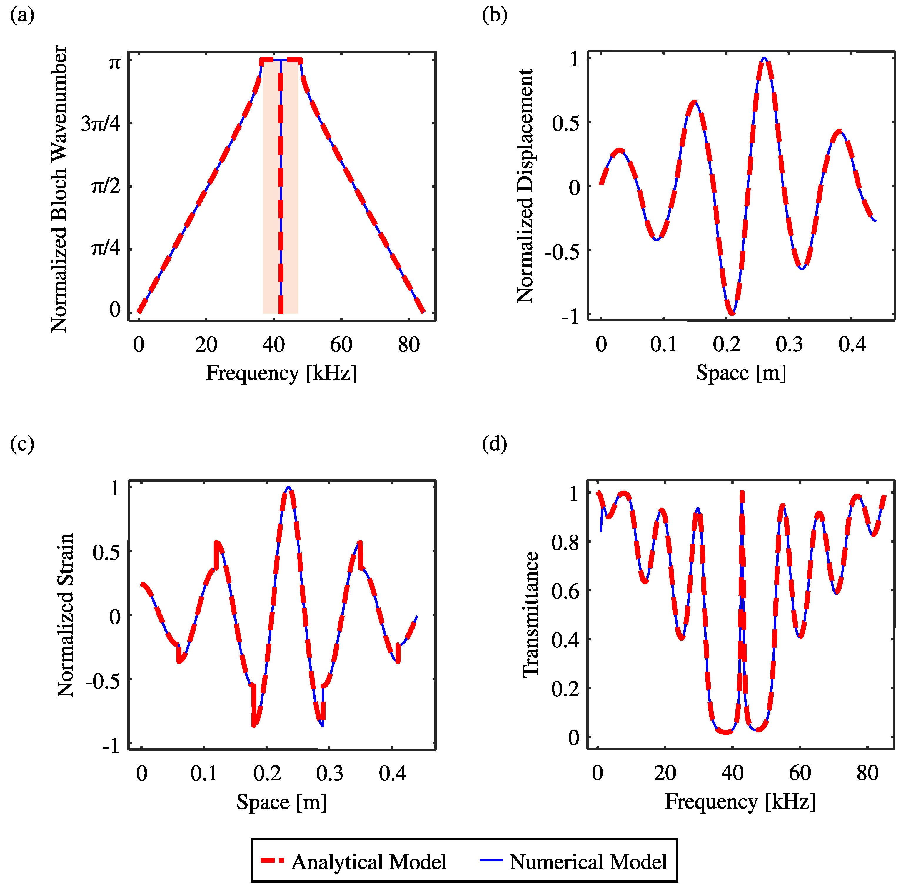
3.2. Prediction in Band Structures and Transmittance FRFs

In the preceding section, two governing equations were formulated to investigate the piezoelectric defect from both mechanical and electrical perspectives, alongside the mechanical equations of motion for the rest of the structure, using the extended Hamilton’s principle. Building on these foundations, the present section introduces a mathematical framework for predicting output responses of defective PnCs, using the explicit solutions derived earlier.
In this work, the transfer-matrix method serves as the computational foundation for predicting both dispersion relations and transmittance FRFs in defective PnCs. In this approach, a one-dimensional structure of homogenous and isotropic material is represented by a 2 × 2 matrix that relates the state vector, comprising mechanical displacement and force, at one boundary to that at the opposite boundary. The transfer-matrix method provides an exact, computationally efficient, and highly modular framework for one-dimensional wave analysis. This framework facilitates the expeditious incorporation of electromechanical coupling and feedback gains at the local level, thereby enabling efficient parameter sweeps that would otherwise be impractical with full finite element models. It is possible to compute band structures by sequentially multiplying these matrices for all cells in a finite or periodic arrangement. This can be achieved by enforcing Bloch-periodic boundary conditions on the global transfer matrix. This process yields dispersion curves and identifies band gaps and defect bands. Furthermore, transmittance FRFs can be obtained by concatenating semi-infinite host matrices with the defective PnC and applying the continuity of displacement and force at each interface. The transfer-matrix framework is readily adaptable to incorporate electroelastic coupling and feedback gains by accounting for the voltage-relevant nonhomogeneous terms within the transfer matrix of the defect. The subsequent analysis employs the transfer-matrix method to generate baseline band diagrams and transmittance FRFs under short-circuit conditions. Subsequently, the model integrates displacement-, velocity-, and acceleration-controlled feedback gains to predict their individual and combined effects on defect-band tuning and filter sensitivity.
The longitudinal wave-specific transfer matrix establishes a relationship between two different quantities (i.e., velocity and force) at both ends—specifically at ‘ x PD = 0 ’ and ‘ x PD = l PD ’—within one-dimensional structures. At any arbitrary spatial position, ‘ x PD ,’ the velocity field ‘ w PD ( x PD , t ) ’ and the corresponding force ‘ f PD ( x PD , t ) ’ are given by the following:
(9a) w PD x PD , t = u PD t , (9b) f PD x PD , t = Y A PD u PD x PD + 2 κ PP 1 + g Disp + i ω g Vel ω 2 g Acc v S .
As indicated in Equation (6a), the displacement field ‘ u PD ( x PD , t ) ’ is expressed with respect to the undetermined displacement coefficients ‘ P PD ’ and ‘ Q PD .’ Consequently, the field quantities in Equation (9a,b) can also be expressed in terms of these coefficients. In this formulation, the 2 × 1 vector representing the velocity and force at any arbitrary spatial position ‘ x PD ’ is obtained by multiplying a 2 × 2 matrix, ‘ CM ( x PD , t ) ,’ which contains the spatial information, and a 2 × 1 vector composed of ‘ P PD ’ and ‘ Q PD .’ Therefore, the velocity and force at the two ends arise solely from changing the spatial information embedded in the 2 × 2 matrix ‘ CM ( x PD , t ) ,’ enabling the derivation of the transfer matrix as follows:
(10a) w PD 0 , t f PD 0 , t = C M PD 0 , t P PD Q PD , w PD l PD , t f PD l PD , t = C M PD l PD , t P PD Q PD , (10b) T M PD = C M PD l PD , t C M PD 0 , t 1 .
The following equation provides a concise explanation of the explicit form of the transfer matrix TM PD ( g Disp , g Vel , g Acc ) for the piezoelectric defect, derived through the process outlined below:
(11a) T M PD g Disp , g Vel , g Acc = cos β PD l PD j sin β PD l PD Z PD j Z PD sin β PD l PD cos β PD l PD + η PD ( g Disp , g Vel , g Acc ) sin β PD l PD j Z PD 1 + cos β PD l PD j Z PD 1 cos β PD l PD sin β PD l PD , (11b) η PD ( g Disp , g Vel , g Acc ) = 2 κ PP 2 1 + g Disp + i ω g Vel ω 2 g Acc ω Z PD 1 cos k PD l PD C PP + 2 κ PP 2 1 + g Disp + i ω g Vel ω 2 g Acc ω Z PD sin k PD l PD ,
where the physical quantity ‘ η PD ( g Disp , g Vel , g Acc ) ’ refers to the electroelastic coupling coefficient in terms of the transfer matrix. The mechanical coupling arising from the bonding effects of the bimorph piezoelectric devices is encapsulated by the effective wavenumber ‘ β PD ’ and the effective mechanical impedance ‘ Z PD .’ Concurrently, the physical quantity ‘ η PD ( g Disp , g Vel , g Acc ) ’ also accounts for the piezoelectric coupling through the coefficient ‘ e PP ’ (or ‘ κ PP ’) and incorporates the gains ‘ g Disp ,’ ‘ g Vel ,’ and ‘ g Acc ,’ which are central to the proposed feedback control strategy. The primary contribution of this study is the introduction of a novel electroelastically coupled transfer matrix that integrates active feedback control. It is further anticipated that the influence of active feedback control will be distinctly observable in both the band structure analysis—based on the transfer matrix method—and the transmittance analysis—employing the S-parameter method—which both utilize this advanced transfer matrix formulation. Additionally, it is noteworthy that the transfer matrix can be simplified to that of metallic structures, as demonstrated below:
T M n = cos β n l n j Z n sin β n l n j Z n sin β n l n cos β n l n ,
where the subscript ‘n’ is constrained to the set {UL, UD}.
As illustrated in Figure 2a,b, the band-structure analysis focuses on two distinct structures: one unit cell and one defective PnC. Two key assumptions are commonly adopted for both structures. First, the velocity and force are continuous at the internal interfaces—i.e., at regions where the material composition varies—ensuring that these fields remain continuous throughout the structure. Second, the field quantities at both ends of each structure satisfy periodic boundary conditions, as prescribed by Floquet–Bloch theory. The integration of these assumptions leads to the following set of eigenvalue problems:
(13a) T M U e j β U Bloch l U I w U 0 , t f U 0 , t = 0 , (13b) T M PnC e j β PnC Bloch l PnC I w PnC 0 , t f PnC 0 , t = 0 , (13c) T M U = T M UD T M UL , (13d) T M PnC g Disp , g Vel , g Acc = T M U N D T M PD g Disp , g Vel , g Acc T M UL T M U D 1 .
In this context, the normalized Bloch wavenumber, denoted as ‘ β l ,’ is real-valued and extends from zero to π [44].
This study utilizes a combination of eigenvalue and eigenvector analyses to investigate the characteristics of phononic band gaps, defect-band frequencies, and defect-mode shapes. The natural frequencies, represented by the eigenvalues in Equation (13a,b), are evaluated as functions of the normalized Bloch wavenumber. In the case of the unit cell, Equation (13a) reveals phononic band gaps, which correspond to frequency ranges that do not appear for any given set of normalized Bloch wavenumbers. By focusing on the frequencies within these band gaps, Equation (13b) then uncovers the defect-band frequencies in defective PnCs that persist across all normalized Bloch wavenumbers—even within the identified band gaps. This stepwise approach is predicated on the underlying principles that govern defect-band formation. This approach—analyzing band gaps in smaller structures and then investigating defect bands in larger systems—provides a time-efficient alternative to performing a comprehensive band-structure analysis across a wide frequency range in larger systems.
Subsequently, the eigenvector derived from Equation (13b) at each defect-band frequency provides the velocity and force at the left boundary (i.e., w PnC ( 0 , t ) and f PnC ( 0 , t ) ). These values form the basis for determining two displacement coefficients in the initial light gray substructure, which then fully specify its displacement field. By applying continuity conditions, the velocity and force at the left boundary of the adjacent dark-gray substructure can be similarly established, thereby defining its displacement field. Repeating this procedure across all substructures of the defective PnC yields the complete displacement field—corresponding to the defect-mode shape. Additional field variables, such as the strain field, can be subsequently evaluated.
In Figure 2c, the S-parameter method is employed in this study to evaluate the frequency response function (FRF) for transmittance. In the front region ( x SL 0 ), the displacement field is represented by ‘ A SL e ( j ( ω t β SL x SL ) ) + B SL e ( j ( ω t + β SL x SL ) ) .’ In the rear region ( x SL 0 ), the displacement field is given by ‘ A SR e ( j ( ω t β SR x SR ) ) .’ The points of ‘ x SL = 0 ’ and ‘ x SR = 0 ’ define the boundaries between the defective PnC and the adjoining semi-infinite regions. The relationship among the displacement coefficients ‘ A SL ,’ ‘ B SL ,’ and ‘ A SR ,’ is established using a 2 × 2 scattering matrix, denoted as ‘ SM PnC ( g Disp , g Vel , , g Acc ) ,’ as shown in Equation (14a). By enforcing the continuity of velocity and force, the scattering matrix ‘ SM PnC ( g Disp , g Vel , g Acc ) ’ can be expressed as the product of the defective PnC-level transfer matrix ‘ TM PnC ( g Disp , g Vel , g Acc ) ’ and the matrices ‘ CM SL ( 0 , t ) ’ and ‘ CM SR ( 0 , t ) ,’ as presented in Equation (14b). Similarly, the 2 × 2 matrix ‘ CM ’ introduced in Equation (10a) defines the relationship between the displacement coefficients within a region and the velocity and force at a specific point in that region. Accordingly, ‘ CM SL ( 0 , t ) ’ and ‘ CM SR ( 0 , t ) ’ are the matrices calculated at the rightmost of the left semi-infinite structure and the leftmost of the right semi-infinite structure, respectively:
(14a) A SR 0 = S M PnC g Disp , g Vel , g Acc A SL B SL , (14b) S M PnC g Disp , g Vel , g Acc = C M SR 0 , t 1 T M PnC g Disp , g Vel , g Acc C M SL 0 , t .
Finally, the transmittance FRF can be given by the following:
A SR g Disp , g Vel , g Acc A SL 2 = det S M PnC g Disp , g Vel , g Acc S M PnC ( g Disp , g Vel , g Acc ) 2 , 2 2 .

4. Effectiveness of Active Feedback Control for Tunable Bandpass Filters

4.1. Numerical Settings for Case Studies

The numerical parameters used in the case studies are delineated, preceding a detailed evaluation of the efficacy of active feedback control in implementing an electrically tunable bandpass filter. Section 4.2 analyzes a configuration in which a defect takes place in the fourth unit cell of a seven-cell array—that is, N = 7 and D = 4 . This parameter setting is reflected in Figure 2, with light gray representing magnesium and dark gray indicating aluminum. For the piezoelectric layers, PZT-5H, a material that has found wide application in piezoelectric sensors and actuators, is employed, while brass serves as the substrate in the bimorph piezoelectric devices. A similar bimorph configuration composed of these materials is detailed in Refs. [45,46,47]. The material properties and geometric specifications are summarized in Table 1, with the corresponding datasheet provided by COMSOL Multiphysics 6.2.
To obtain the band structure and transmittance FRFs using the analytical model described in Section 3, the parameters detailed in Table 1 are substituted into Equations (1a)–(15). One key benefit of this analytical model is its ability to rapidly yield phononic band gaps, defect-band frequencies, defect-mode shapes, and transmittance FRFs across various combinations of the gains ‘ g Disp ,’ ‘ g Vel ’, and ‘ g Acc .’ Although the model is based on several assumptions and may not achieve absolute precision, it is expected to generate results that closely approximate those produced by the numerical model within a specified frequency range. In this study, the analytical model was implemented in MATLAB R2025a, while numerical simulations were performed using COMSOL Multiphysics 6.2. The utilization of COMSOL in the field of PnCs is noteworthy, given its proficiency in multiphysics problems. For a comprehensive exposition on the capabilities of COMSOL Multiphysics in conducting band structure and transmittance analyses, we direct the reader to the Supplementary Material. The computational setup included a MAG B650M MORTAR WIFI motherboard, an AMD Ryzen 9 7900X CPU, a Manli Nebula GeForce RTX 5070 12 GB GDDR7 GPU, and Micron Crucial DDR5-5600 CL46 RAM.

4.2. Tunability Performance Assessment

4.2.1. Preliminary Study Without Active Feedback Control

At the outset, the band structure and transmittance FRF are analyzed without the intervention of active feedback control. In this configuration, the piezoelectric layers remain electrically inert, ensuring that no voltage is generated or applied. Consequently, the manifestation of mechanical bonding effects is constrained to the defect. Within the analytical model, the piezoelectric effects are effectively disabled by setting the piezoelectric coupling coefficient ‘ e PP ’ to zero. This adjustment effectively nullifies the electroelastic coupling coefficient at the transfer-matrix level, designated as ‘ η PD ( g Disp , g Vel , g Acc ) ’ in Equation (11b). Within the COMSOL framework, an analogous outcome is attained by characterizing the piezoelectric material as an anisotropic elastic material. The ensuing results are illustrated in Figure 3.
As illustrated in Figure 3a, the band-structure results derived from both methods are presented. The red dashed lines illustrate the analytical model’s predictions, whereas the blue solid lines delineate the COMSOL simulation results. According to the analytical model, the band-gap frequency spans from 35.47 to 47.98 kHz, punctuated by an interstitial defect band occurring at approximately 42.78 kHz. In contrast, the COMSOL simulations reveal a band gap extending from 35.46 to 47.97 kHz, with a corresponding defect-band frequency also approximating 42.77 kHz. A noteworthy observation is the close alignment between the band gap limits and defect-band frequencies derived from these two approaches, with discrepancies confined to a margin of error of less than 1%.
Figure 3b,c further illustrate the defect-mode shape at the defect-band frequency, revealing a striking agreement between the analytical model and the COMSOL simulation. Specifically, Figure 3b,c illustrate the displacement and strain fields of the defective PnC, respectively. It is noteworthy that the displacement field exhibits nearly perfect point symmetry, while the strain field demonstrates almost perfect line symmetry surrounding the epicenter of the piezoelectric defect. As delineated in Equation (4c,d), this symmetrical attribute is of paramount importance [36]. This symmetry guarantees that the electrical circuit equations yield a valid electric current or voltage by requiring a nonzero displacement disparity between the two extremities of the piezoelectric defect. Consequently, the manner in which the wave energy becomes localized within the piezoelectric defect fundamentally governs the activation of piezoelectric phenomena. The point-symmetric nature of the displacement field (or line-symmetric nature of the strain field) not only serves as an ideal platform for demonstrating piezoelectric effects but also reinforces the relevance of the present case study for exploring active feedback control strategies.
As illustrated in Figure 3d, the transmittance FRF is presented using the same line and color conventions as observed in the preceding figures. It is noteworthy that both modeling approaches yield results that are in remarkable agreement. In this approach, both methods undertake a frequency sweep in 10 Hz increments over a predetermined frequency range, employing a sequential analysis at each step. While COMSOL simulations may require up to an hour to complete, the analytical model delivers its results in mere seconds. This substantial discrepancy underscores the potential of the proposed analytical framework for future applications, particularly in scenarios demanding real-time automatic adjustments of gain in response to external frequency variations. Furthermore, the analysis of both models indicates that an almost perfect transmission is achieved within the narrow frequency region centered on the previously identified defect-band frequency. Conversely, frequencies slightly outside this critical band exhibit near-zero transmittance. This phenomenon is indicative of a bandpass filter based on the defect mode. The primary objective of this study is to electrically manipulate the peak frequency, specifically the defect-band frequency, of this bandpass filter through the implementation of active feedback control. An additional note is that the narrowband capability can be further enhanced by increasing the mechanical impedance difference of the structures within cells or by arranging more cells.

4.2.2. Scenario I—Active Feedback Control Effects of Respective Gains

In this subsection, the variation of the defect-band frequency and the corresponding transmittance value concerning each gain is examined. Specifically, a single gain is varied, while the other two are held constant at zero. The three gain types are displacement-controlled ( g Disp ), velocity-controlled ( g Vel ), and acceleration-controlled ( g Acc ) factors, respectively. Given the analysis in the previous subsection—that the peak frequency in the transmittance FRF coincides with the defect-band frequency in the band structures—the ensuing discussion focuses exclusively on the peak frequency.
As illustrated in Figure 4, a comprehensive synopsis of the findings is provided across six panels. Figure 4a,b illustrate the changes in the peak frequency and the corresponding transmittance value as functions of the displacement-controlled gain ‘ g Disp .’ Figure 4c,d demonstrate these variations for the velocity-controlled gain ‘ g Vel ,’ while Figure 4e,f depict the responses for the acceleration-controlled gain ‘ g Acc .’ In all cases, the red dashed line indicates the results obtained from the analytical model, whereas the blue solid line represents the outcomes from the COMSOL simulations. The x-axis of each figure ranges from negative to positive values, representing the full spectrum of gain variations, while the y-axis captures the frequency ranges (in Figure 4a,c,e) within the band-gap region or the transmittance values (in Figure 4b,d,f). This detailed representation underscores the robustness of the proposed approach in characterizing the electrically tunable energy-localized behavior of defective PnCs with active feedback control, reinforcing the consistency between the analytical predictions and the numerical simulation results. In addition, Figure 4 presents the computed results for all possible combinations of gain and frequency over different ranges—an iterative process that is particularly computationally intensive. In the event that the sweep interval for each gain is set to 1 and the sweep interval for frequency is set to 10 Hz, the proposed analytical model produces results in just ten seconds per figure, whereas COMSOL simulations with identical settings require one or more days. This substantial decrease in computation time validates the efficacy and efficiency of the proposed model.
Starting from Figure 4a,b, a monotonic variation in the peak frequency is evident as the displacement-controlled gain ‘ g Disp ’ undergoes a range of values from −90 to 90. With respect to the zero-valued gain condition, an increase in the gain in the positive direction results in a continuous increase in the peak frequency until it finally disappears when the upper limit of the band gap is reached. Conversely, an increase in the gain in the negative direction results in a continuous decrease in the peak frequency until it disappears at the lower limit of the band gap. This behavior indicates that the active feedback control strategy allows for the arbitrary selection of the operating frequency for the tunable bandpass filter over a wide range within the phononic band gap by allowing for the free adjustment of the degree of electroelastic coupling within the piezoelectric defect. As demonstrated in Figure 4b, this strategy ensures full transmission efficiency, thereby maintaining the functionality of the system.
As illustrated in Figure 4c,d, the outcomes associated with the velocity-controlled gain, denoted by ‘ g Vel ,’ substantially deviate from those attained with the displacement-controlled gain, ‘ g Disp .’ It is important to note that the velocity-controlled gain ‘ g Vel ’ exerts a direct influence on the imaginary part of the electroelastic coupling coefficient, ‘ η PD ( g Disp , g Vel , g Acc ) ,’ within the transfer-matrix formulation. Two notable observations emerge from Figure 4c. First, the peak frequency remains nearly constant as the velocity-controlled gain varies; as the gain transitions from 15 × 10 5 to point 10 × 10 5 , the peak frequency shifts only within a narrow band from 42.86 to 43.36 kHz. Despite this limited variation, the peak eventually disappears when the velocity-controlled gain reaches specific positive and negative threshold values—frequencies that do not correspond to the boundaries of the band gap. Next, Figure 4d reveals an important finding regarding the transmittance values under the influence of the velocity-controlled gain ‘ g Vel ’. When the gain is initially set to zero, an increase in positive gain leads to a monotonically decreasing transmittance, eventually reaching zero. In contrast, an increase in negative gain results in a dramatic increase in transmittance that levels off after a certain threshold (in this study, 2 × 10 5 ).
Turning to Figure 4e,f, the results obtained with acceleration-controlled gain, ‘ g Acc ,’ reveal both similarities and differences when compared to the outcomes derived from displacement-controlled gain, ‘ g Disp .’ Of particular note is the electroelastic coupling coefficient, denoted as ‘ η PD ( g Disp , g Vel , g Acc ) ,’ which demonstrates that the acceleration-controlled gain ‘ g Acc ’ is multiplied by ω 2 prior to its application. Two significant observations emerge from Figure 4e. First, a monotonic variation in the peak frequency is observed over a specified range of ‘ g Acc .’ For positive gain values, the peak frequency decreases monotonically as the gain increases, whereas for negative gain values, the peak frequency increases monotonically with increasing gain. This behavior is particularly noteworthy because the acceleration-controlled gain ‘ g Acc ’ produces the opposite trend relative to the displacement-controlled gain ‘ g Disp .’ Second, the multiplication by ω 2 results in the heightened sensitivity of the peak frequency to variations in ‘ g Acc ,’ compared to the response observed with ‘ g Disp .’ Furthermore, Figure 4f demonstrates that the transmittance value remains constant at one regardless of the acceleration-controlled gain value ‘ g Acc .’
In summary, the defect-band frequency and the transmission amplitude are influenced by each feedback gain. The displacement-controlled gains are illustrated in Figure 4a,b, while the acceleration-controlled gains are shown in Figure 4e,f. It is evident that increasing either of these gains results in a discernible, monotonic shift in the defect-band frequency. Despite this frequency tuning, the transmission amplitude remains equal to the short-circuit (baseline) value, indicating pure frequency control without affecting bandpass filtering magnitude. In the case of velocity-controlled gains illustrated in Figure 4c,d, adjustments to the velocity-controlled gain exert minimal influence on the defect-band frequency. Instead, these adjustments alter the steepness and height of the transmission peak. This phenomenon exemplifies a form of sensitivity control, whereby the bandpass response undergoes a process of sharpening or flattening, while the fundamental frequency remains relatively unaltered.

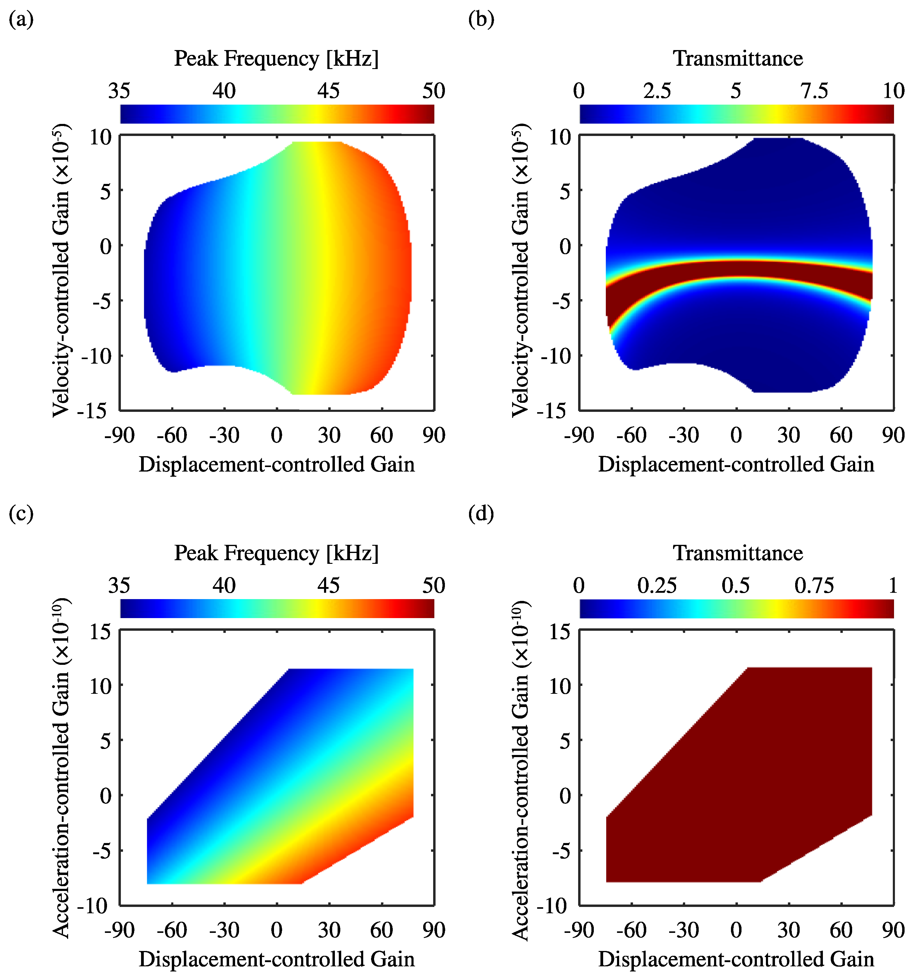
4.2.3. Scenario II—Active Feedback Control Effects of Combined Gains

The preceding section examines the scenario with a single activated gain; the present section extends this analysis to the scenario with two simultaneously activated gains. The results of the aforementioned study can be summarized as follows. The tuning of the defect-band frequency is influenced by both displacement- and acceleration-controlled gains, ‘ g Disp ’ and ‘ g Acc .’ Conversely, the velocity-controlled gain ‘ g Vel ’ exerts a predominant influence on the peak transmittance value. Numerical simulations across a broad range of gain and frequency combinations demonstrate excellent agreement with the proposed analytical model. This validation serves as a foundational step in the direction of an analytical focus on two-gain configurations. The initial configuration assesses the combined impact of displacement- and velocity-controlled gains, ‘ g Disp ’ and ‘ g Vel .’ The second configuration examines the combined effects of displacement- and acceleration-controlled gains, ‘ g Disp ’ and ‘ g Acc .’ It is noteworthy that the findings from the displacement-velocity scenario provide sufficient information about the behavior observed when velocity- and acceleration-controlled gains, ‘ g Vel ’ and ‘ g Acc ,’ are both activated.
Figure 5 shows the results of the combination study. The same gain ranges examined in Figure 4 are applied to evaluate three different two-gain-frequency configurations. All simulations are completed in under twenty minutes, demonstrating computational efficiency suitable for embedding on microcontrollers in real-world applications. While simplifying assumptions may introduce inaccuracies, on-the-fly parameter tuning or model calibration can mitigate any resulting errors. These results further validate the system’s practicality and readiness for deployment.
Figure 5a,b illustrate the dependence of both peak frequency (i.e., defect-band frequency) and peak transmittance value on the displacement- and velocity-controlled gains, ‘ g Disp ’ and ‘ g Vel .’ While every gain combination was evaluated, blank (white) regions denote parameter sets that produce no detectable peak within the predefined band gap. As the displacement-controlled gain ‘ g Disp ’ increases, the peak frequency increases in a consistent manner for a constant-controlled velocity gain ‘ g Vel .’ This relationship is illustrated in Figure 4. In a similar manner, for a fixed displacement-controlled gain ‘ g Disp ,’ the peak frequency vanishes before or after a certain value as the velocity-controlled gain varies ‘ g Vel .’ Interestingly, an unexpected finding emerges from the combination study. In the absence of displacement-controlled gain, i.e., when ‘ g Disp ’ is zero, the velocity-controlled gain ‘ g Vel ’ exerts negligible influence on the defect-band frequency. However, as the displacement-controlled gain ‘ g Disp ’ deviates from zero, the effects of the velocity-controlled gain ‘ g Vel ’ become increasingly pronounced. This results in discernible shifts in the peak frequency. Next, Figure 5b shows that, for any displacement-controlled gain ‘ g Disp ’, there exists a range of velocity-controlled gains ‘ g Vel ’ over which the transmittance exceeds 10, appearing as a distinct red zone. Overlaying this zone onto Figure 5a reveals that particular combinations of displacement- and velocity-controlled gains, ‘ g Disp ’ and ‘ g Vel ,’ both amplify the sensitivity of the narrow bandpass filter and allow for the continuous tuning of the defect-band frequency across the entire phononic bandgap. This capability markedly enhances the performance of remotely tunable bandpass filters and underscores the practical significance of the combination study.
Subsequently, Figure 5c,d illustrate the variation of peak frequency and peak transmittance with displacement- and acceleration-controlled gains, ‘ g Disp ’ and ‘ g Acc .’ As illustrated in Figure 5c, the variation trends of the peak frequency are characterized by a high degree of linearity. Specifically, at a constant displacement-controlled gain ‘ g Disp ,’ an increase in the acceleration-controlled gain ‘ g Acc ’ results in a decrease in the peak frequency. Conversely, at a fixed acceleration gain ‘ g Acc ,’ an increase in the displacement-controlled gain ‘ g Disp ’ leads to an increase in the peak frequency. The dominance of one gain, therefore, determines whether the defect-band frequency shifts up or down, and for certain gain pairs, it even moves outside the band gap. Conversely, Figure 5d demonstrates a uniform transmittance of 1 for all gain combinations. This finding suggests that, while this gain configuration enables the continuous tuning of the defect-band frequency, it does not enhance filter sensitivity.

5. Conclusions

The present study introduces an analytical framework for predicting and electrically tuning defect-relevant characteristics in one-dimensional phononic crystals (PnCs) via active feedback control. The defect-band frequency was shown to shift continuously across the entire band gap when paired piezoelectric sensors and actuators were embedded within the defect, and three independently adjustable feedback gains (displacement, velocity, and acceleration) were applied. The transfer matrix-based analytical model demonstrated sub-percent accuracy relative to COMSOL benchmarks, with relative differences below 1% in both the defect band and transmittance analyses. Notably, the computational time was significantly reduced from hours to seconds, thereby enabling rapid parametric sweeps over the gain and frequency domains. Such rapid sweeps would be impractical with full multiphysics simulations.
Key findings include the following:
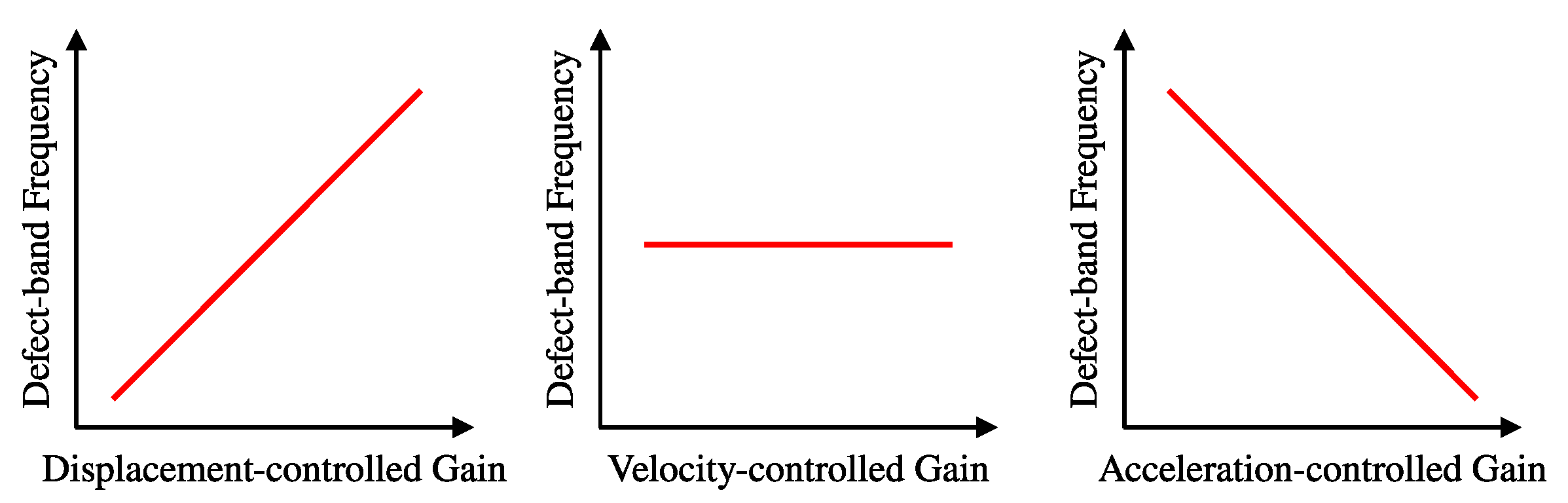
  • Displacement-controlled gain facilitated a unidirectional adjustment of the defect-band frequency, either in an upward or a downward direction, across the entire band gap. Concurrently, this gain ensures the preservation of nearly unity transmittance. Positive gain increased the peak frequency, thereby raising it towards the upper band gap frequency. Conversely, negative gain was demonstrated to decrease the peak frequency, thereby lowering it to the lower band gap frequency.
  • Acceleration-controlled gain generated frequency shifts that were opposite in sign to those from the displacement-controlled gain. This resulted in heightened sensitivity due to the frequency-squared weighting. Nevertheless, complete transmission efficiency was maintained.
  • Velocity-controlled gain was designed to maintain a constant peak frequency while facilitating a wide-range modulation of the transmittance. This innovative feature enabled independent tuning of the filter sensitivity without the need to adjust the operating frequency, thereby enhancing the system’s flexibility and reliability.
  • Combined gains provided synergistic control. Displacement- and velocity-controlled gains permitted the concurrent manipulation of the defect-band frequency and enhancement of the bandpass filtering sensitivity. Conversely, displacement- and acceleration-controlled gains enabled highly linear control of the defect-band frequency without compromising sensitivity. These synergistic effects achieved multi-objective filter reconfiguration.
As part of ongoing research, three control strategies will be implemented and evaluated within a unified experimental framework. First, a passive inductive-resistive circuit will establish the baseline response of the defective PnC. Next, a semi-active configuration featuring a synthetic negative capacitor realized with operational amplifiers will demonstrate intermediate tunability. Ultimately, the incorporation of active configurations that facilitate real-time feedback loops between embedded sensors and actuators will enable real-time and remote defect-band modulation.
The following advantages of the proposed analytical feedback-control approach should be emphasized. First, the analytical model is proposed as a replacement for full multiphysics simulations. This modification has the result that defect-band frequencies and transmittance can now be computed in seconds rather than hours. This, in turn, enables true real-time tunability under changing operating conditions. Second, gain-frequency maps that formerly necessitated days of finite element analysis are now generated in mere seconds, thereby facilitating rapid parametric studies and on-the-fly optimization as stimulus frequencies fluctuate. Finally, the closed-form formulation is sufficiently lightweight to be deployed on low-power microcontrollers, thereby enabling remote, on-demand filter reconfiguration without the need for manual circuitry modifications.
In practice, three main challenges can arise when deploying the analytical transfer-matrix approach. First, sensors and actuators exhibit non-negligible bandwidth limits, electrical and mechanical damping, and measurement noise. Ensuring that the controller gains are implemented without inducing instability (e.g., oscillations or drift) will require a careful design of analog/digital amplifiers and filtering stages. Second, variations in piezoelectric coupling coefficients, adhesive layers, or substrate geometry will shift the true defect-band frequencies and modify the effective mechanical impedance. Addressing these uncertainties necessitates the implementation of an on-site calibration procedure or the utilization of adaptive control algorithms. These algorithms are designed to identify and rectify instances of parameter drift. Lastly, at high gains, the piezoelectric material or the amplifier may enter nonlinear regimes (saturation, hysteresis), and thermal effects (Joule heating in the circuit, hysteretic heating in the ceramics) can alter both electrical and mechanical properties. In order to ensure reliable operation in demanding environments, it is imperative to extend the analytical model to include these nonlinearities or to bind them with robust control techniques. In summary, while the mathematical approach promises sub-percent accuracy and millisecond-scale tuning, implementing it in hardware will demand careful attention to dynamical stability, component tolerances, and nonlinearities.
Future endeavors will encompass the following: (i) the experimental validation of the analytical model under diverse environmental and loading conditions; (ii) the extension of active feedback control schemes to two- and three-dimensional defective PnC architectures; (iii) the incorporation of geometric and material nonlinearities, stochastic material imperfections, and higher-order wave-motion effects for advanced analytical formulation and experimental validation; (iv) the optimization of multi-objective feedback-controller design for robust, real-time operation in the presence of uncertainty; and (v) the integration of the active tuning mechanism into distributed, adaptive sensing networks to enable fully autonomous filter reconfiguration.

Supplementary Materials

The following supporting information can be downloaded at: https://www.mdpi.com/article/10.3390/math13132126/s1, Derivation of Governing Equations and Description of COMSOL Simulation Settings.

Funding

This work was supported by the Basic Science Research Program through the National Research Foundation of Korea (NRF), funded by the Ministry of Education under Grant 2022R1I1A1A01056406.

Data Availability Statement

The original contributions presented in this study are included in the article. Further inquiries can be directed to the corresponding author.

Conflicts of Interest

The author declares no conflicts of interest.

References

  1. Dong, H.W.; Shen, C.; Liu, Z.; Zhao, S.D.; Ren, Z.; Liu, C.X.; He, X.; Cummer, S.A.; Wang, Y.S.; Fang, D.; et al. Inverse design of phononic meta-structured materials. Mater. Today 2024, 80, 824–855. [Google Scholar] [CrossRef]
  2. Huang, W.; Xu, J.; Yao, Y.; Zhang, Y.; Wang, X.; Han, P. Application of phononic crystals in modern engineering vibration and noise control, a review. Noise Vib. Worldw. 2025, 56, 09574565251333071. [Google Scholar] [CrossRef]
  3. Lee, J.; Kim, Y.Y. Elastic metamaterials for guided waves: From fundamentals to applications. Smart Mater. Struct. 2023, 32, 123001. [Google Scholar] [CrossRef]
  4. Akbari-Farahani, F.; Ebrahimi-Nejad, S. From defect mode to topological metamaterials: A state-of-the-art review of phononic crystals & acoustic metamaterials for energy harvesting. Sens. Actuators A Phys. 2024, 365, 114871. [Google Scholar]
  5. Hu, G.; Tang, L.; Liang, J.; Lan, C.; Das, R. Acoustic-elastic metamaterials and phononic crystals for energy harvesting: A review. Smart Mater. Struct. 2021, 30, 085025. [Google Scholar] [CrossRef]
  6. Jam, M.T.; Shodja, H.M.; Sanati, M. Band-structure calculation of SH-waves in 1D hypersonic nano-sized phononic crystals with deformable interfaces. Mech. Mater. 2022, 171, 104359. [Google Scholar] [CrossRef]
  7. Hu, J.; Dong, P.; Cao, J.; Gong, Z.; Hou, R.; Yuan, H. Dynamic bandgap responsiveness of modified re-entrant metamaterials in thermal-mechanical field. J. Mater. Res. Technol. 2024, 30, 7328–7339. [Google Scholar] [CrossRef]
  8. Jiang, Z.; Zhang, F.; Li, K.; Chai, Y.; Li, W.; Gui, Q. A multi-physics overlapping finite element method for band gap analyses of the magneto-electro-elastic radial phononic crystal plates. Thin-Walled Struct. 2025, 210, 112985. [Google Scholar] [CrossRef]
  9. Zhang, S.; Bian, X. Tunable defect states of flexural waves in magnetostrictive phononic crystal beams by magneto-mechanical-thermal coupling loadings. Thin-Walled Struct. 2024, 199, 111848. [Google Scholar] [CrossRef]
  10. Hao, Y.; Huo, Y.; Zhang, W. Locally resonant metamaterial plate with cantilever spiral beam-mass resonators and various piezoelectric defects for energy harvesting. Thin-Walled Struct. 2025, 213, 113259. [Google Scholar] [CrossRef]
  11. Yao, B.; Wang, S.; Hong, J.; Gu, S. Size and temperature effects on band gap analysis of a defective phononic crystal beam. Crystals 2024, 14, 163. [Google Scholar] [CrossRef]
  12. Shen, N.; Cong, Y.; Gu, S.; Zhang, G.; Feng, Z.Q. Design of phononic crystals using superposition of defect and gradient-index for enhanced wave focusing. Smart Mater. Struct. 2024, 33, 085034. [Google Scholar] [CrossRef]
  13. Gao, X.; Qin, J.; Hong, J.; Wang, S.; Zhang, G. Wave propagation characteristics and energy harvesting of magnetically tunable defective phononic crystal microbeams. Acta Mech. 2025, 236, 1579–1597. [Google Scholar] [CrossRef]
  14. Jo, S.H.; Yoon, H.; Shin, Y.C.; Youn, B.D. Revealing defect-mode-enabled energy localization mechanisms of a one-dimensional phononic crystal. Int. J. Mech. Sci. 2022, 215, 106950. [Google Scholar] [CrossRef]
  15. He, Z.; Zhang, G.; Chen, X.; Cong, Y.; Gu, S.; Hong, J. Elastic wave harvesting in piezoelectric-defect-introduced phononic crystal microplates. Int. J. Mech. Sci. 2023, 239, 107892. [Google Scholar] [CrossRef]
  16. Zhang, G.; Gao, X.; Wang, S.; Hong, J. Bandgap and its defect band analysis of flexoelectric effect in phononic crystal plates. Eur. J. Mech.-A/Solids 2024, 104, 105192. [Google Scholar] [CrossRef]
  17. Xiao, J.; Ding, X.; Huang, W.; He, Q.; Shao, Y. Rotating machinery weak fault features enhancement via line-defect phononic crystal sensing. Mech. Syst. Signal Process. 2024, 220, 111657. [Google Scholar] [CrossRef]
  18. Sepehri, S.; Mashhadi, M.M.; Fakhrabadi, M.M.S. Active/passive tuning of wave propagation in phononic microbeams via piezoelectric patches. Mech. Mater. 2022, 167, 104249. [Google Scholar] [CrossRef]
  19. Jin, Y.; Torrent, D.; Rouhani, B.D.; He, L.; Xiang, Y.; Xuan, F.Z.; Gu, Z.; Xue, H.; Zhu, J.; Wu, Q.; et al. The 2024 phononic crystals roadmap. J. Phys. D Appl. Phys. 2025, 58, 113001. [Google Scholar] [CrossRef]
  20. Ji, G.; Huber, J. Recent progress in acoustic metamaterials and active piezoelectric acoustic metamaterials-a review. Appl. Mater. Today 2022, 26, 101260. [Google Scholar] [CrossRef]
  21. Khalid, M.Y.; Arif, Z.U.; Tariq, A.; Hossain, M.; Umer, R.; Bodaghi, M. 3D printing of active mechanical metamaterials: A critical review. Mater. Des. 2024, 246, 113305. [Google Scholar] [CrossRef]
  22. Zhang, X.; Li, Y.; Wang, Y.; Jia, Z.; Luo, Y. Narrow-band filter design of phononic crystals with periodic point defects via topology optimization. Int. J. Mech. Sci. 2021, 212, 106829. [Google Scholar] [CrossRef]
  23. Lucklum, R.; Mukhin, N. Enhanced sensitivity of resonant liquid sensors by phononic crystals. J. Appl. Phys. 2021, 130, 024508. [Google Scholar] [CrossRef]
  24. Na, K.; Kim, Y.; Yoon, H.; Youn, B.D. FASER: Fault-affected signal energy ratio for fault diagnosis of gearboxes under repetitive operating conditions. Expert Syst. Appl. 2024, 238, 122078. [Google Scholar] [CrossRef]
  25. Kim, H.; Park, C.H.; Suh, C.; Chae, M.; Oh, H.J.; Yoon, H.; Youn, B.D. Stator current operation compensation (SCOC): A novel preprocessing method for deep learning-based fault diagnosis of permanent magnet synchronous motors under variable operating conditions. Measurement 2023, 221, 113446. [Google Scholar] [CrossRef]
  26. Yang, J.; Jo, S.H. Experimental validation for mechanically tunable defect bands of a reconfigurable phononic crystal with permanent magnets. Crystals 2024, 14, 701. [Google Scholar] [CrossRef]
  27. Li, Y.; Zhang, X.; Gao, Z.; Luo, Y.; Wang, R. Topology optimization of wide-Frequency tunable phononic crystal resonators with a reconstructable point defect. Adv. Theory Simulations 2025, 2401441. [Google Scholar] [CrossRef]
  28. Zhang, G.; He, Z.; Wang, S.; Hong, J.; Cong, Y.; Gu, S. Elastic foundation-introduced defective phononic crystals for tunable energy harvesting. Mech. Mater. 2024, 191, 104909. [Google Scholar] [CrossRef]
  29. Linyang, G.; Xiaohui, M.; Zhaoqing, C.; Chunlin, X.; Jun, L.; Ran, Z. Tunable a temperature-dependent GST-based metamaterial absorber for switching and sensing applications. J. Mater. Res. Technol. 2021, 14, 772–779. [Google Scholar] [CrossRef]
  30. Geng, Q.; Fong, P.K.; Ning, J.; Shao, Z.; Li, Y. Thermally-induced transitions of multi-frequency defect wave localization and energy harvesting of phononic crystal plate. Int. J. Mech. Sci. 2022, 222, 107253. [Google Scholar] [CrossRef]
  31. Jo, S.H. Temperature-controlled defective phononic crystals with shape memory alloys for tunable ultrasonic sensors. Crystals 2025, 15, 412. [Google Scholar] [CrossRef]
  32. Zhang, S.; Zhang, Z. Magnetically tunable band gaps and defect states of longitudinal waves in hard magnetic soft phononic crystal beams. Eur. J. Mech.-A/Solids 2025, 111, 105575. [Google Scholar] [CrossRef]
  33. Zhang, S.; Bian, X. Magneto-mechanical-thermal coupling tunability of the topological interface state of longitudinal waves in magnetostrictive phononic crystal beams. Mech. Syst. Signal Process. 2024, 212, 111286. [Google Scholar] [CrossRef]
  34. Shakeri, A.; Darbari, S.; Moravvej-Farshi, M. Designing a tunable acoustic resonator based on defect modes, stimulated by selectively biased PZT rods in a 2D phononic crystal. Ultrasonics 2019, 92, 8–12. [Google Scholar] [CrossRef] [PubMed]
  35. Taleb, F.; Darbari, S. Tunable locally resonant surface-acoustic-waveguiding behavior by acoustoelectric interaction in Zn O-based phononic crystal. Phys. Rev. Appl. 2019, 11, 024030. [Google Scholar] [CrossRef]
  36. Jo, S.H.; Park, M.; Kim, M.; Yang, J. Tunable bandpass filters using a defective phononic crystal shunted to synthetic negative capacitance for longitudinal waves. J. Appl. Phys. 2024, 135, 164502. [Google Scholar] [CrossRef]
  37. Jo, S.H. Electrically controllable and reversible coupling degree in a phononic crystal with double piezoelectric defects. Thin-Walled Struct. 2024, 204, 112328. [Google Scholar] [CrossRef]
  38. Mao, J.; Gao, H.; Zhu, J.; Gao, P.; Qu, Y. Analytical modeling of piezoelectric meta-beams with unidirectional circuit for broadband vibration attenuation. Appl. Math. Mech. 2024, 45, 1665–1684. [Google Scholar] [CrossRef]
  39. Zhou, W.; Chen, W.; Chen, Z.; Lim, C. Actively controllable flexural wave band gaps in beam-type acoustic metamaterials with shunted piezoelectric patches. Eur. J. Mech.-A/Solids 2019, 77, 103807. [Google Scholar] [CrossRef]
  40. Wang, X.; Song, L.; Xia, P. Active control of adaptive thin-walled beams incorporating bending-extension elastic coupling via piezoelectrically induced transverse shear. Thin-Walled Struct. 2020, 146, 106455. [Google Scholar] [CrossRef]
  41. Erturk, A.; Inman, D.J. Piezoelectric Energy Harvesting; John Wiley & Sons: Hoboken, NJ, USA, 2011. [Google Scholar]
  42. Yoon, H.; Youn, B.D.; Kim, H.S. Kirchhoff plate theory-based electromechanically-coupled analytical model considering inertia and stiffness effects of a surface-bonded piezoelectric patch. Smart Mater. Struct. 2016, 25, 025017. [Google Scholar] [CrossRef]
  43. Huang, B.; Kim, H.S.; Yoon, G.H. Modeling of a partially debonded piezoelectric actuator in smart composite laminates. Smart Mater. Struct. 2015, 24, 075013. [Google Scholar] [CrossRef]
  44. Shen, W.; Cong, Y.; Gu, S.; Yin, H.; Zhang, G. A generalized supercell model of defect-introduced phononic crystal microplates. Acta Mech. 2024, 235, 1345–1360. [Google Scholar] [CrossRef]
  45. Leadenham, S.; Erturk, A. Unified nonlinear electroelastic dynamics of a bimorph piezoelectric cantilever for energy harvesting, sensing, and actuation. Nonlinear Dyn. 2015, 79, 1727–1743. [Google Scholar] [CrossRef]
  46. Sadaf, A.I.; Ahmed, R.U.; Ahmed, H. Cantilever configurations in vibration-based piezoelectric energy harvesting: A comprehensive review on beam shapes and multi-beam formations. Smart Mater. Struct. 2024, 33, 123001. [Google Scholar] [CrossRef]
  47. Erturk, A.; Inman, D.J. An experimentally validated bimorph cantilever model for piezoelectric energy harvesting from base excitations. Smart Mater. Struct. 2009, 18, 025009. [Google Scholar] [CrossRef]
Figure 1. Expected tuning of the defect-band frequency under different feedback gains. The defect-band frequency will increase monotonically with displacement-controlled gain, remain constant with velocity-controlled gain, and decrease monotonically with acceleration-controlled gain.
Mathematics 13 02126 g001
Figure 2. Schematic overview of a one-dimensional defective PnC with active feedback control for electrically tunable bandpass filters. (a) The band-gap analysis at the unit-cell level: The dispersion relation of the periodic structure delineates the frequency ranges wherein wave propagation is prohibited. (b) The defect-band analysis at the defective PnC level: The introduction of a local defect engenders narrow passbands within the band gap, thereby illustrating the spatial localization via defect modes. (c) The transmittance analysis for a defective PnC with two semi-infinite structures: The corresponding transmittance spectrum highlights the isolated peaks at each defect-band frequency. (d) Active feedback control loop: Real-time voltage output from piezoelectric sensors is processed by a controller and fed back as an input voltage to piezoelectric actuators. This dynamic feedback loop enables the precise modulation of defect-band frequency and filter sharpness.
Mathematics 13 02126 g002
Figure 3. Comparison of analytical (red dashed) and numerical (blue solid) predictions for a defective PnC without electroelastic coupling. (a) Bloch wavenumber–frequency diagram: The shaded region in the figure delineates the phononic band gap, while the vertical line indicates the defect-band frequency at which a localized defect-mode exists. (b) Normalized displacement profile at the defect-band frequency: This phenomenon is indicative of substantial energy localization to the area of the defect. (c) Normalized strain field distribution at the defect-band frequency: This phenomenon signifies the maximum strain experienced at the defect site and the subsequent rapid propagation to neighboring host cells. (d) Transmittance FRF for a finite defective PnC with semi-infinite structures: The presence of a single sharp transmission peak at the defect band frequency is indicative of the accuracy of the transfer matrix predictions, as confirmed by the excellent overlap between the analytical and numerical curves.
Mathematics 13 02126 g003
Figure 4. Analytical (red dashed) versus numerical (blue solid) predictions of active feedback control effects for individual feedback gains (Scenario I). (a,b) Displacement-controlled gain effects: (a) A monotonic upward shift of the defect-band frequency as the gain increases, with excellent agreement between analytical and numerical results, and (b) constant peak transmittance at the short-circuit level despite variations in gains, demonstrating pure frequency tuning. (c,d) Velocity-controlled gain effects: (c) A negligible change in the defect-band frequency across the range of gains, indicating decoupled sensitivity control, and (d) a significant modulation of peak transmittance with gains, demonstrating adjustable filter sharpness independent of frequency. (e,f) Acceleration-controlled gain effects: (e) A monotonic downward shift of the defect-band frequency with increasing gain, which closely matches both analytical and numerical predictions, and (f) stable peak transmittance at the baseline level as the gain varies, confirming that the gain controls frequency without altering filtering magnitude.
Mathematics 13 02126 g004
Figure 5. Analytical predictions of active feedback control effects for combined gains (Scenario II). (a,b) Displacement- and velocity-controlled gain effects: (a) Defect-band frequency variation under simultaneous adjustment of the combined gains, showing a predictable upward shift dominated by the displacement-controlled gain with a negligible frequency drift from the velocity-controlled gain, and (b) peak transmittance modulation under the combined gains, illustrating that the velocity-controlled gain tailors filter sharpness while the displacement-controlled gain has minimal impact on amplitude. (c,d) Displacement- and acceleration-controlled gain effects: (c) Defect-band frequency shifts resulting from the combined gains, demonstrating additive tuning actions—upward by the displacement-controlled gain and downward by the acceleration-controlled gain—with analytical and numerical curves in strong agreement, and (d) peak transmittance remains constant across varied, combined gains, confirming that combined frequency tuning does not affect filtering sensitivity.
Mathematics 13 02126 g005
Table 1. Detailed information of system parameters, material properties, and geometric specifications.
System parameters
The number of unit cells, N 7
Defect location, D 4
Mechanical properties
MagnesiumDensity, ρ UL 1770 kg/m3
Elastic constant, Y UL 45 GPa
AluminumDensity, ρ UD 2700 kg/m3
Elastic constant, Y UD 70 GPa
BrassDensity, ρ PS 8730 kg/m3
Elastic constant, Y PS 91 GPa
PZT-5HDensity, ρ PP 7500 kg/m3
Elastic constant, Y PP 60.6 GPa
Electrical properties
PZT-5HPiezoelectric coupling coefficient, e PP −16.6 C/m2
Dielectric constant, ε PP S 25.55 nF/m
Geometric dimensions
WidthOverall structure, w PnC 5 mm
LengthLight gray structure, l UL 30 mm
Dark gray structure, l UD 30 mm
Piezoelectric defect, l PD 50 mm
HeightDefective PnC, h PnC 5 mm
Substrate, h PS 0.2 mm
Piezoelectric layer, h PP 0.2 mm
Disclaimer/Publisher’s Note: The statements, opinions and data contained in all publications are solely those of the individual author(s) and contributor(s) and not of MDPI and/or the editor(s). MDPI and/or the editor(s) disclaim responsibility for any injury to people or property resulting from any ideas, methods, instructions or products referred to in the content.

