Article

Defect-Band Splitting of a One-Dimensional Phononic Crystal with Double Defects for Bending-Wave Excitation

1
Department of Mechanical, Robotics, and Energy Engineering, Dongguk University, Seoul 04620, Republic of Korea
2
Department of Mechanical Engineering, Seoul National University, Seoul 08826, Republic of Korea
3
Institute of Advanced Machines and Design, Seoul National University, Seoul 08826, Republic of Korea
*
Author to whom correspondence should be addressed.
Mathematics 2023, 11(18), 3852; https://doi.org/10.3390/math11183852
Submission received: 18 August 2023 / Revised: 4 September 2023 / Accepted: 7 September 2023 / Published: 8 September 2023
(This article belongs to the Special Issue Analytical Simulation of Structural Dynamics and Vibration)

Abstract

:
Extensive prior research has delved into the localization of elastic wave energy through defect modes within phononic crystals (PnCs). The amalgamation of defective PnCs with piezoelectric materials has opened new avenues for conceptual innovations catering to energy harvesters, wave filters, and ultrasonic receivers. A recent departure from this conventional paradigm involves designing an ultrasonic actuator that excites elastic waves. However, previous efforts have mostly focused on single-defect scenarios for bending-wave excitation. To push the boundaries, this research takes a step forward by extending PnC design to include double piezoelectric defects. This advancement allows ultrasonic actuators to effectively operate across multiple frequencies. An analytical model originally developed for a single-defect situation via Euler–Bernoulli beam theory is adapted to fit within the framework of a double-defect set-up, predicting wave-excitation performance. Furthermore, a comprehensive study is executed to analyze how changes in input voltage configurations impact the output responses. The ultimate goal is to create ultrasonic transducers that could have practical applications in nondestructive testing for monitoring structural health and in ultrasonic imaging for medical purposes.

1. Introduction

Phononic crystals (PnCs) have captured substantial interest in contemporary research [1,2]. They consist of specifically designed unit cells arranged in a periodic fashion, enabling researchers to push the limits of technology in controlling the flow (e.g., propagating direction and energy density) of elastic waves. A fascinating area of exploration focuses on localizing and amplifying wave energy in specific regions by intentionally introducing one or more defects in PnCs [3,4]. The ordered arrangement of unit cells in defect-free PnCs plays a crucial role in creating band gaps through Bragg scattering, which occurs when propagating waves interact with periodic structures [5,6]. It is essential to clarify that when we mention ‘a single defect’, we refer to an engineered situation where one unit cell’s geometric values and/or material are altered. This introduction of a single defect leads to the formation of passbands inside the band gaps. These bands are called as ‘defect bands’, which are characterized by nearly flat slopes [7,8]. Consequently, the respective defect bands manifest resonating motions of the defect, called ‘defect-mode shapes’. Such a fascinating nature opens the door for a high level of localization of elastic waves within the unwanted areas.
Recent explorations have been dedicated to understanding the consequences of ‘double defects’ in elastic domains [9,10]. Double defects involve the introduction of an additional defect with the same configuration as the initial defect but positioned differently within the PnC. Within this context, researchers have discovered two remarkable phenomena. First, each defect band, which materializes when a single defect is present, undergoes a captivating split, resulting in the formation of two distinct bands. Second, both defects showcase the occurrence of energy concentration at their respective split defect bands. Here, one intriguing point is that they demonstrate differing symmetric behaviors (line symmetry versus point symmetry) in their respective displacement/velocity/stress/strain fields. These remarkable traits have been corroborated through theoretical simulations and experimental demonstrations [11,12]. These characteristics empower a PnC integrated with double defects to function as a potent amplifier of mechanical energy across several frequencies, surpassing the capabilities of the previous single-defect method.
Furthermore, integrating piezoelectric materials, renowned for their intelligent properties [13,14], into the design step of defective PnCs starts devising various engineering prototypes that harness the potential of defect-mode-induced wave localization [15,16,17,18]. These piezoelectric materials can serve as useful defects themselves or be strategically attached to defect sites. Throughout this paper, a defect containing a piezoelectric material is termed a ‘piezoelectric defect’. Within this domain, two primary research themes have emerged. The first one involves amplifying electrical outputs generated through direct piezoelectric effects. Researchers aim to enhance the efficiency and sensitivity of energy conversion [19,20]. The second one centers on environmentally controlling the properties of defect bands, which represent narrowband regions with high values in the frequency–response curve of the transmittance of mechanical power [21,22]. Engineers can achieve environment-adaptive wave propagation and power transmission through defective PnCs. These research areas primarily revolve around scenarios in which incident elastic waves interact with defective PnCs. Notably, considerable regard has been directed toward devising energy harvesters, ultrasonic receivers, and bandpass filters.
A groundbreaking shift has recently emerged in a novel area of research, focused on exciting and amplifying elastic waves through converse piezoelectric effects [23,24]. In contrast to the aforementioned themes, this topic explores scenarios where piezoelectric materials are exposed to external input voltage sources, with the goal of advancing ultrasonic actuators. However, this area shows promising potential with only a handful of studies conducted so far. To demonstrate the significant impact of defective PnCs on the excitation of longitudinal waves, two analytical approaches rooted in the Rayleigh–Love theory have been presented [25,26]. These approaches account for single or double defects. Additionally, an initial analytical approach based on the fundamental Euler–Bernoulli beam theory has been introduced to showcase the bending-wave-excitation phenomenon and to improve its output performance compared to cases without defective PnCs [27]. In simulations, the velocity amplitude of generated bending waves is amplified nearly ten times. However, the investigation of bending-wave excitation has been limited to scenarios involving a single defect. Addressing this research gap becomes the driving force behind the present study, aiming to expand the understanding of bending-wave-excitation behaviors within PnCs with double defects.
Hence, the primary objective of this endeavor is to devise an advanced ultrasonic actuator concept, which harnesses the double-defect modes inherent in a one-dimensional PnC for the explicit purpose of exciting bending waves. The overarching goal here is to facilitate efficient operation at not just one, but two or potentially multiple frequencies by skillfully capitalizing on the distinct characteristics of defect-band splitting. This research is centered on two pivotal aspects: (i) developing an analytical approach to predict the wave-excitation performance of a PnC containing double piezoelectric defects via the Euler–Bernoulli beam theory [27] and (ii) confirming the enhancement of the output performance compared to scenarios in which the PnC is not present. The analytical approach under consideration is based on the transfer-matrix and scattering parameter methods, which are well-known mathematical techniques in circuit theory and waveguide modeling [28,29]. These approaches require the derivation of governing equations (e.g., wave equation and electrical circuit equation) and their explicit solutions. To corroborate the proposed analytical approach’s validity and efficacy, a comparative study is conducted, pitting its outcomes against results obtained via the finite element method [30,31]. The salient advantage of this analytical approach lies in its ability to considerably reduce computation time while retaining exceptional predictive capabilities, well within the bounds of acceptable ranges defined by underlying modeling assumptions.
Section 2 introduces the target system of an advanced ultrasonic actuator concept, employing a double-piezoelectric-defect arrangement. Section 3 and Section 4 elaborate on the enhanced analytical approach tailored for the double-defect case and provide corresponding numerical validation results, respectively. In Section 5, the summary of this study is presented, along with a listing of potential future avenues that can further advance the field of ultrasonic actuators incorporating defective PnCs.

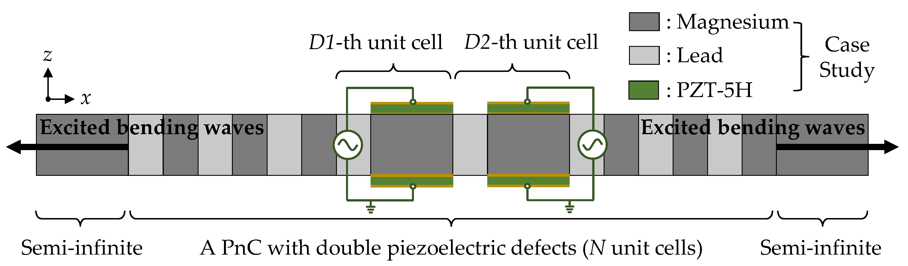
2. Target System Description

Figure 1 illustrates a one-dimensional system featuring a double-defect-introduced PnC, where bimorph piezoelectric elements are externally placed at each defect site to excite bending waves. These piezoelectric elements comprise piezoceramic materials (e.g., PZT (lead zirconate titanate)), while metallic materials comprise the remaining beams. The unit cell consists of two beams represented by light and dark gray colors, respectively, with all beams, except for the piezoelectric elements, having a constant rectangular cross-section. Arranging N unit cells along the 1-axis forms a defect-free PnC. To create double defects within the PnC, the lengths of the dark beams in the D1-th and D2-th unit cells (where D2 > D1) are modified in a same manner. Note that the physical quantities D1 and D2 present the order (integer number) of the unit cells in which each defect is introduced. Two identical dark green piezoelectric elements, sharing the same configuration and specification, are layered onto the upper and lower surfaces of each defect, covering the entire region. Gold-colored electrodes are positioned on the top and bottom of each piezoelectric element. In the engineering set-up, semi-infinite dark gray beams are attached at both ends of the PnC with double piezoelectric defects, enabling bending waves to propagate outward without reflections caused by finite conditions. This configuration facilitates the analysis of the unique wave-excitation capabilities of the PnC with double piezoelectric defects. Previous research has demonstrated that the occurrence of defect-mode-enabled wave localization and defect-band splitting in defective PnCs is independent of whether finite or semi-infinite conditions are considered, and this has been confirmed through numerical analysis and experiments [11].
In this system, all piezoelectric elements undergo 3-axial electric polarization, brought to life by independent external input voltage sources, vPD1(t) and vPD2(t). Each voltage source is linked between the uppermost and lowermost surfaces of each piezoelectric defect using electric cables, electrically connecting the two elements in series while the elements are mechanically positioned in parallel [32]. The intrigue lies in the opposite signs of their respective piezoelectric coupling coefficients. Consequently, each element in the piezoelectric defect experiences contrasting mechanical deformations. This is the piezoelectric elements’ basic principle of 31-mode-based bending-wave excitation [33,34].
Notations bearing the subscripts ‘DU’, ‘LU’, ‘D’, ‘P’, ‘LS’, and ‘RS’ indicate the physical attributes of the dark and light gray beams within the unit cell, the defect, the piezoelectric element, and the left and right semi-infinite structures, respectively. Here, one defect and the enclosed bimorph piezoelectric elements behave as one equivalent beam, thanks to the assumption of perfect bonding. Then, the notations bearing the subscript ‘PD’ pertain to their equivalent characteristics. In detail, the subscripts ‘PD1′ and ‘PD2′ correspond to the piezoelectric defects positioned at D1-th and D2-th unit cells, respectively. The notation ‘l’ denotes the length. The unit-cell size ‘lUC’ is lDU + lLU. The overall length ‘lPnC’ of the PnC is computed as NlUnit + 2(lPDlDU). Apart from four piezoelectric elements, the height of each beam is represented by ‘hPnC’. The notation ‘wPnC’ designates the overall width. It is noteworthy that the slenderness ratio ‘l/h’ should be the same as or exceeds ten in compliance with assumptions of the Euler–Bernoulli beam theory [35]. The notations ‘S’ and ‘I’ stand for the cross-sectional area and the second moment of area, respectively. The notations ‘ρ’ and ‘Y’ signify the mass density and Young’s modulus of the metals, respectively. The notations ‘ c 11 E ’, and ‘e31’ for the piezoelectric elements denote the 1-axial elastic modulus and the piezoelectric coupling coefficient, respectively.
The physical quantities under analysis can be classified into two categories. The first involves quantifying defect bands and examining their defect-mode shapes through dispersion analysis without input voltage sources. This analysis will be presented in Section 3.1 and Section 4.2. The second category focuses on quantifying the velocity amplitude of waves computed at the semi-infinite beams during wave-excitation analysis with input voltage sources. Section 3.2 and Section 4.3 elaborate on this analysis.

3. Transfer-Matrix- and S-Parameter-Based Analytical Approaches

3.1. Transfer-Matrix-Method-Based Prediction in Dispersion Analysis

Throughout this paper, the Cartesian coordinate system is considered. In both space and time, the transverse displacement along the 3-axis is described as ‘u(x, t)’. Keeping in mind the Euler–Bernoulli beam theory, we embark upon the mathematical derivation of the angular rotation (spatial slope), internal bending moment, and shear force, symbolized by ‘θ(x, t)’, ‘m(x, t)’, and ‘q(x, t)’, respectively [36]. These quantities come from the first, second, and third spatial derivatives of the transverse displacement u(x, t), respectively. It is important to note that this paper follows a specific sign convection. The internal shear force q(x, t) is the negative of the third derivative of the transverse displacement u(x, t), while all other field quantities have a positive sign. For a simple beam in the absence of an input voltage, this aspect can be summarized as [37]:
θ x , t = u x , t x , m x , t = YI 2 u x , t x 2 , q x , t = YI 3 u x , t x 3 .
A detailed description of the modeling assumptions and setting is provided in Appendix A. This appendix covers the derivation of governing equations for bending waves and their transverse displacement solutions in the presence and absence of the piezoelectric effects.
A transfer matrix, labeled as ‘TM’, is a powerful mathematical entity that elucidates the explicit correlation between designated field quantities computed at the opposing terminations of a given, one-dimensional structure [35,38,39,40]. The governing equation defined in Equation (A4) for bending waves stands as a fourth-order partial (or ordinary) differential equation, resulting in the development of a 4 × 4 transfer matrix. In this paper, we direct our attention towards four crucial physical parameters, namely transverse displacement u(x, t), angular rotation θ(x, t), internal bending moment m(x, t), and internal shear force q(x, t). Additionally, the spotlight shines solely on a unit cell or a double-defect-introduced PnC, driven by the desire to discern their innate characteristics through the investigation of their dispersion relations. Consequently, the presence of semi-infinite structures and input voltage source is deliberately disregarded. Therefore, only the homogenous solution in the transverse displacement is taken into account. Note that the superscript ‘DA’ succinctly abbreviates the realm of dispersion analysis.
The transfer-matrix approach presented here is a versatile method applicable to all beams, even when considering the presence of piezoelectric defects without input voltage sources. To simplify notation, the subscripts are omitted. The first step involves establishing a 4 × 4 matrix ‘FMDA(x, ω)’ that builds a connection between the vector encompassing these four field quantities and another vector comprising four transverse displacement coefficients at an arbitrary space x. By utilizing this FMDA(x, ω), we derive a specialized 4 × 4 transfer matrix TMDA(ω), specifically designed to describe bending waves in each beam, as follows:
T M DA ω = F M DA x = l , ω F M DA x = 0 + , ω 1 ,
where the matrix FMDA(x, ω) can be readily derived with the help of Equation (1) as:
F M DA x , ω = D M DA ω C M DA x , ω ,
D M DA ω = 1 0 0 0 0 1 0 0 0 0 YI 0 0 0 0 YI ,
C M DA x , ω = exp kx exp kx exp jkx exp jkx kexp kx kexp kx jkexp jkx jkexp jkx k 2 exp kx k 2 exp kx k 2 exp jkx k 2 exp jkx k 3 exp kx k 3 exp kx j k 3 exp jkx j k 3 exp jkx .
Of significant importance is the critical assumption regarding the continuous nature of the four field quantities along the periodic beams. This assumption plays a vital role in ensuring smooth continuity at each interface where different beam materials intersect, resulting in a simplified calculation process for transfer matrices at both the unit cell and PnC with double piezoelectric defects. To be precise, we refer to these transfer matrices as ‘ T M DPnC DA ω DPnC ’ and ‘ T M DPnC DA ω DPnC ’, as they serve to establish the definitive correlation between the four field quantities located at the extreme left and right of the unit cell (with the subscript ‘UC’) and defective PnC (with the subscript ‘DPnC’), respectively, as follows:
T M UC DA ω UC = T M DU DA ω UC T M LU DA ω UC ,
T M DPnC DA ω DPnC = T M UC DA ω DPnC N D 2 T M PD 2 DA ω DPnC T M LU DA ω DPnC × T M UC DA ω DPnC D 2 D 1 1 T M PD 1 DA ω DPnC T M LU DA ω DPnC × T M UC DA ω DPnC D 1 1 .
To successfully utilize the supercell technique, leveraging the Floquet–Bloch theorem becomes imperative [3]. This involves formulating two distinct eigenvalue problems, as illustrated below:
T M UC DA ω UC exp j k UC DA l UC I 4 × 4 f q UC DA x UC = 0 + , ω UC = 0 4 × 1 ,
T M DPnC DA ω DPnC exp j k DPnC DA l DPnC I 4 × 4 f q DPnC DA x DPnC = 0 + , ω DPnC = 0 4 × 1 ,
where the 4 × 4 identity matrix represented by ‘I4×4’ and the 4 × 1 zero vector denoted as ‘04×1’ hold significant importance. The 4 × 1 vector ‘fq’ conveniently holds the values of four distinct field quantities at an arbitrary spatial position. Additionally, ‘xUC = 0+’ and ‘xDPnC = 0+’ explicitly indicates each left end. The normalized Bloch wavenumbers, ‘ k UC DA ’ and ‘ k DPnC DA ’, are constrained to the interval between zero to π. To find the dispersion curves for both the unit cell and the PnC with double piezoelectric defects, a numerical solution of the characteristic equation (Equations (8) and (9)) yields normalized Bloch wavenumbers linked to eigenvalues at each frequency. This computational approach facilitates the visualization of the respective dispersion curves. Notably, Equation (8) serves to identify band gaps, which correspond to frequency ranges that deviate from real-valued Bloch wavenumbers. Conversely, Equation (9) effectively pinpoints defect bands, where real-valued Bloch wavenumbers are present, but exclusively within the confines of the band gaps. Additionally, upon solving the eigenvalue problem at the PnC level, an eigenvector emerges, each associated with different defect-band frequencies. The initial beam is the starting point, wherein the transverse displacement coefficients are determined and the displacement field is specified by multiplying the eigenvector with the inverse of the matrix F M LU DA ( x LU DA = 0+, ωDPnC). Subsequently, the resulting eigenvector is further multiplied by the transfer matrix T M LU DA (ωDPnC) of the initial beam, yielding field quantities at the left end of the next beam. By repeatedly applying this process for each beam, the overall transverse displacement field, commonly referred to as the defect-mode shape, can be obtained.

3.2. Prediction in Wave-Excitation Analysis

This study centers on the examination under the influence of input voltage sources. While the preceding section employs the transfer-matrix method, we now introduce the S-parameter method. This method represents an enhanced version of the transfer-matrix technique, meticulously tailored to situations that encompass external inputs (e.g., forces). The S-parameter method elucidates distinct attributes that distinguish it from the previous section [41,42,43,44]. First, it crucially incorporates the nonhomogeneous solution, accounting for piezoelectric coupling effects, denoted in Equation (A6). Second, notable adjustments are applied to the vectors or matrices of fqDA, FMDA, and TMDA, with specific adaptations to accommodate input voltage sources. Last, a perceptive consideration arises, addressing the impact of semi-infinite host beams on the landscape of wave excitation and propagation. As a side note, the superscript ‘WA’ succinctly abbreviates the realm of wave-excitation analysis.
Within this context, a newly established 6 × 1 vector, denoted as fqWA(x, ω), comes into prominence. Its exact formulation is delineated as fqWA(x, ω)= [uWA (x, ω); θWA (x, ω); mWA(x, t); qWA(x, ω); vPD1(ω); v PD2(ω)]. It is of paramount significance to underscore that the input voltages vPD1(ω) and vPD2(ω) retain their status as user-defined scalar quantities. In contrast, the remaining constituents, entailing evaluative computation, encapsulate the field variables contingent upon the spatial coordinate x and the frequency ω. The introduction of these input voltages necessitates adjustments to the field properties characterized by the angular rotation θWA(x, ω), internal bending moment mWA(x, ω), and internal shear force qWA(x, ω), as elaborated upon subsequently:
θ a WA = d u a WA d x a , m a WA = YI PD d 2 u a WA d x a 2 κ P v a , q a WA = YI PD d 3 u a WA d x a 3 , θ b WA = d u b WA d x b , m b WA = Y b I PnC d 2 u b WA d x b 3 , q b WA = Y b I PnC d 3 u b WA d x b 3 .
It is pertinent to recall that the transverse displacement fields, denoted as u PD 1 WA (xPD1, ω) and u PD 2 WA (xPD2, ω), are inherently underpinned by a nonhomogeneous solution. In contrast to the procedure in dispersion analysis, it is noteworthy that Equation (10) presents supplementary terms, represented as κPvPD1(ω) and κPv PD2(ω), within the context of internal bending moments. This distinctive characteristic imparts discernible alterations to the matrices of significance.
The transfer matrix, denoted as TMWA(ω) takes on the structure of a 6 × 6 matrix. This matrix serves a pivotal role as it establishes a link between two 6 × 1 vectors, namely fqWA(x = 0+, ω) assessed at the left end of a beam, and fqWA(x = l, ω) computed at its right end. In a parallel manner to the discussion in Section 3.2, a redefined form of the 6 × 6 matrix FMWA(x, ω), is tailored to seamlessly integrate with the current context. This refined matrix configuration gives rise to the modified transfer matrix TMWA(ω), encompassing:
T M WA ω = F M WA x = l , ω F M WA x = 0 + , ω 1 ,
where FMWA(ω) can be readily derived with the assistance of Equation (10) leading to:
F M WA x , ω = D M WA ω C M WA x , ω ,
D M a WA ω = D M a DA ω P D M a WA 0 2 × 4 I 2 × 2 , D M b WA ω = D M b DA ω 0 4 × 2 0 2 × 4 I 2 × 2 ,
C M a WA x a , ω = C M a DA x a , ω P C M a WA x a , ω 0 2 × 4 I 2 × 2 , C M b WA x b , ω = C M b DA x b , ω 0 4 × 2 0 2 × 4 I 2 × 2 ,
where the 4 × 2 matrices P D M PD1 WA , P D M PD2 WA , P C M PD1 WA (xPD1, ω), and P C M PD2 WA (xPD2, ω) are expressed as:
P D M PD1 WA = 0 0 0 0 κ P 0 0 0 , P C M PD1 WA x PD 1 , ω = u PD1 , NH WA x PD1 , ω 0 d u PD1 , NH WA x PD1 , ω d x PD1 0 d 2 u PD1 , NH WA x PD1 , ω d x PD1 2 0 d 3 u PD1 , NH WA x PD1 , ω d x PD1 3 0 ,
P D M PD2 WA = 0 0 0 0 0 κ P 0 0 , P C M PD2 WA x PD2 , ω = 0 u PD2 , NH WA x PD1 , ω 0 d u PD2 , NH WA x PD2 , ω d x PD2 0 d 2 u PD2 , NH WA x PD2 , ω d x PD2 2 0 d 3 u PD2 , NH WA x PD2 , ω d x PD2 3 .
Reverting to the transfer matrix TMWA(ω), it serves as the intermediary connecting six distinct physical entities. These encompass four attributes pertaining to the field, alongside two input voltages, strategically positioned at each extremity of the PnC with double piezoelectric defects. By adhering to the principle of continuity, these very same six variables can also be ascertained at the distant rightmost point of the semi-infinite host beam on the left side, and similarly at the remote leftmost juncture of the semi-infinite host beam on the right side. Consequently, the waves that become excited within these semi-infinite host beams unveil the expressions denoting the transverse displacement field, as presented herewith:
u c WA x c , ω = P c , HY WA ω exp k c ω x c + Q c , HY WA ω exp k c ω x c     + P c , TR WA ω exp j k c ω x c + Q c , TR WA ω exp j k c ω x c ,
where the subscript ‘c’ belongs to the set {LS, RS}. Next, we engage a scattering matrix denoted as SMWA(ω). This scattering matrix adopts the structure of a 6 × 6 array, operating as a conduit connecting two distinct 6 × 1 vectors. The first vector comprises the coefficients that signify the transverse displacement, along with the input voltage, localized at the first (or second) piezoelectric defect. The second vector encompasses the four coefficients for transverse displacement and the input voltage associated with each respective semi-infinite host beam. By leveraging the principle of continuity and employing advanced mathematical methodologies, a sequence of matrices, denoted as SMWA(ω), can be systematically derived as follows:
S M LS WA ω = F M LS WA x LS = 0 + , ω 1 T M UC WA ω 1 D 1 × T M LU WA ω 1 F M PD1 WA x PD1 = 0 + , ω ,
S M RS WA ω = F M RS WA x RS = 0 + , ω 1 T M UC WA ω N D 2 × T M PD2 WA ω T M LU WA ω T M UC WA ω D 2 D 1 1 F M PD1 WA x PD1 = l PD , ω .
It should be mentioned that Equations (18) and (19) aim to establish a connection between the first piezoelectric defect and semi-infinite host beams. The modification of the formulations in Equations (18) and (19) to consider the second piezoelectric defect, in lieu of the preceding one, is also allowable. As we progress, it becomes imperative to accommodate the distinctive attributes of the semi-infinite host beams. It is evident that the leftward host beam should exclusively accommodate propagating waves and evanescent waves directed towards the left. Similarly, our focus shifts to the rightward host beam, where the consideration revolves around propagating waves that travel along the right direction and evanescent waves whose amplitude exponentially decays along the right direction. This implies that the values of the displacement coefficients PLS,HY(ω), PLS,TR(ω), QRS,HY(ω), and QRS,TR(ω), as outlined in Equation (17), should all be rendered null. These coefficients are associated with reflective waves and hold no significance within this context. By harnessing this understanding and substituting it into Equations (18) and (19), a distinct set of four equations is derived. Consequently, we establish a pathway to ascertain the transverse displacement coefficients for the first piezoelectric defect. These coefficients are expressed through the following equations:
P PD1 , HY WA ω Q PD1 , HY WA ω P PD1 , TR WA ω Q PD1 , TR WA ω = S M LS WA ω 1 , 1 S M LS WA ω 1 , 4 S M LS WA ω 3 , 1 S M LS WA ω 3 , 4 S M RS WA ω 2 , 1 S M RS WA ω 2 , 4 S M RS WA ω 4 , 1 S M RS WA ω 4 , 4 1 × S M LS WA ω 1 , 5 S M LS WA ω 1 , 6 S M LS WA ω 3 , 5 S M LS WA ω 3 , 6 S M RS WA ω 2 , 5 S M RS WA ω 2 , 6 S M RS WA ω 4 , 5 S M RS WA ω 4 , 6 v PD1 ω v PD2 ω .
The pivotal displacement coefficients that define the attributes of the semi-infinite host beams can be systematically determined using the following equation:
Q LS , HY WA ω Q LS , TR WA ω P RS , HY WA ω P RS , TR WA ω = S M LS WA ω 2 , 1 S M LS WA ω 2 , 4 S M LS WA ω 4 , 1 S M LS WA ω 4 , 4 S M RS WA ω 1 , 1 S M RS WA ω 1 , 4 S M RS WA ω 3 , 1 S M RS WA ω 3 , 4 P PD1 , HY WA ω Q PD1 , HY WA ω P PD1 , TR WA ω Q PD1 , TR WA ω + S M LS WA ω 2 , 5 S M LS WA ω 2 , 6 S M LS WA ω 4 , 5 S M LS WA ω 4 , 6 S M RS WA ω 1 , 5 S M RS WA ω 1 , 6 S M RS WA ω 3 , 5 S M RS WA ω 3 , 6 v PD1 ω v PD2 ω .
Notwithstanding their displacement amplitudes, evanescent waves are devoid of the ability to transmit wave energy. Aligning with the solution derived in Equation (21), this study introduces the notion of the wave-excitation performance as the magnitude of transverse velocity observed within propagating waves. This definition holds pertinence when the point of observation is situated at a considerable distance from the PnC with double piezoelectric defects. This concept is quantified through the expressions Q LS , TR WA (ω) and P RS , TR WA (ω), serving as reference points for gauging the efficacy of ultrasonic actuators integrated with defective PnCs.

4. Finite-Element-Method-Based Validation

4.1. Evaluation Setting

In terms of dimensions, both dark and light gray beams are 10 mm in length. Additionally, the piezoelectric defect is 30 mm in length. One piezoelectric element is 0.25 mm in height, while the remaining beams have a height of 1 mm. Aligning with the Euler–Bernoulli beam theory from a structural perspective, each piezoelectric defect maintains a slenderness ratio of 20, whereas the remaining beams uphold a slenderness ratio of 10. Regardless of their type, all beams share a uniform width of 5 mm.
The beams come in two distinct shades: dark gray beams, crafted from magnesium, and light gray beams, composed of lead. The bimorph piezoelectric patches employ PZT-5H as their primary material, a widely favored choice for sensing and actuating systems. Here are the specific details regarding their mechanical and electrical properties: for magnesium, the values are (density, Young’s modulus) = (1770 kg/m3, 45 GPa); for lead, they are (density, Young’s modulus) = (11,340 kg/m3, 16 GPa); and for PZT-5H, the values are (density, elastic constant, piezoelectric coupling coefficient) = (7500 kg/m3, 60.60 GPa, −16.60 C/m2). These values are extracted from the data repository within Comsol Multiphysics 6.1. Note that the simulation setting in Comsol is provided in Appendix B.
The following sections elaborate on the iterative assembly of nine unit cells, leading to the formation of a defect-free PnC. Throughout this process, the lengths of the dark gray beams within the fourth and fifth unit cells are extended, with full-length bimorph piezoelectric elements being affixed. Of importance is the emphasis on the maintenance of structural symmetry within the wave generation system, even when confronted with the presence of double defects. This symmetrical arrangement becomes evident as the double defects are introduced at specific coordinates: (i) D1 = (N + 1)/2 − 1 − K and (N + 2)/2 + K for cases of odd N, where K represents a non-negative integer. This firmly established symmetrical configuration serves a dual purpose. It effectively safeguards against structural influences while simultaneously providing clear insight into the intricate interplay between applied input voltages on individual piezoelectric defects and the resulting velocity amplitude of excited bending waves as they propagate outward. Furthermore, the previous study that investigates the efficacy of the PnC with double piezoelectric defects demonstrates that this specific symmetry configuration exhibits the most favorable performance in exciting longitudinal waves [25,27]. Note that in this scenario of defect introduction, an even number of N always results in a non-symmetric configuration.
It is important to highlight that we have delineated two distinct comparison groups for evaluation. The first group centers on the scenario where the defective PnC is absent. This comparison will be explored in Section 4.3, serving as the foundation for understanding the amplified wave-excitation capabilities conferred by the defective PnC. Conversely, the second comparison group pertains to the single-defect scenario, a configuration of nine unit cells with one defect introduced in the fourth unit cell. Given the inherent non-symmetrical arrangement, noticeable disparities are anticipated in the output responses of the left and right semi-infinite host beams. This particular comparison group will be scrutinized in Section 4.2 and Section 4.3, providing empirical support for the efficacy of defect-band splitting in both dispersion and wave-excitation analyses. As a supplementary observation, it is noteworthy to mention that in the absence of piezoelectric elements, the velocity amplitude remains perpetually at zero due to the non-excitation of waves. This outcome is inherently self-evident and, thus, does not constitute a component of the aforementioned comparison groups.

4.2. Validation Results in Dispersion Analysis

In Figure 2, we observe dispersion curves illustrating three distinct engineering scenarios: the unit cell represented by solid black lines (analytical approach) and black circles (numerical approach), the single-defect case depicted with solid blue lines and blue squares (numerical approach), and the double-defect case shown via solid red lines and blue triangles (numerical approach). Clearly, a distinct band gap emerges, highlighted in gray. When considering the single-defect case, one defect band takes place, which subsequently divides into two distinct defect bands as we transition into the double-defect scenario. The presence of intermediary beams between these double defects gives rise to a mechanical interaction akin to coupling, leading to the intriguing phenomenon of defect-band splitting. This transition from single defect to double defect can be likened to an expansion in the degrees of freedom, akin to observations in vibration engineering when progressing from one to two within the context of a discrete mass–spring system. Figure 3 vividly portrays the defect-mode shapes, showcasing the single- and double-defect scenarios. The outcomes presented through the analytical approach (solid red line in the single-defect scenario and solid blue lines in the double-defect scenario) closely align with those obtained from finite-element-method analysis (dashed black lines), underscoring the analytical method’s meaningfulness. Furthermore, the analytical approach demonstrates impressive computational efficiency, requiring a computation time less of than a second per system. In contrast, the numerical model demands considerably more time, taking 1 min and 4 min for band-gap and defect-band analyses, respectively. This emphasizes the significant advantage of the analytical approach in terms of computational speed for dispersion analysis, while maintaining a high level of predictive accuracy.
Upon examining Figure 2, the proposed analytical approach unveils the appearance of a band gap, spanning from 1.54 kHz to 3.33 kHz. The defect band is precisely identified at 2.45 kHz in the single-defect scenario. Upon the introduction of a double defect, this defect band undergoes a notable split, resulting in two discrete bands: 1.98 kHz and 2.84 kHz. Meanwhile, by employing the finite element method, the calculated values are as follows: 1.54–3.30 kHz for the band gap, 2.44 kHz for a single-defect band, and 1.97 kHz and 2.81 kHz for the split double-defect bands. Remarkably, these outcomes demonstrate negligible relative errors, each very near the 1% margin.
Delving into Figure 3a, a captivating picture unfolds, representing the piezoelectric defect’s capacity to amplify its transverse displacement significantly within the PnC. Notably, this transverse displacement field closely resembles the characteristics of energy-localized behaviors, specifically those characterized by line symmetry. This observation inherently signifies the emergence of energy localization attributed to the single-defect mode. Transitioning to remaining figures, the analogous transverse displacement fields are shown in each piezoelectric defect, mirroring what is depicted in Figure 3a. However, the context of double defects introduces a perspective to focus on, where transverse displacement fields adopt either point- (Figure 3b) or line-symmetric (Figure 3c) patterns with respect to their center situated between the defects. This observation leads to two compelling insights. First, Figure 3b depicts that the double defects operate in perfect synchronization, with both defects concurrently generating maximum or minimum transverse displacements, each in opposing directions, while Figure 3c presents that each defect independently displays both maximum and minimum transverse displacements simultaneously. Second, the maximum transverse displacement occurs at 85 mm in Figure 3a, precisely at the center of the single defect. Conversely, in Figure 3b, the maximum value is located at 89.7 mm, and in Figure 3c, it is situated at 81.8 mm within the first piezoelectric defect. The intricate interaction between the double defects introduces a subtle location difference of approximately 4 mm.

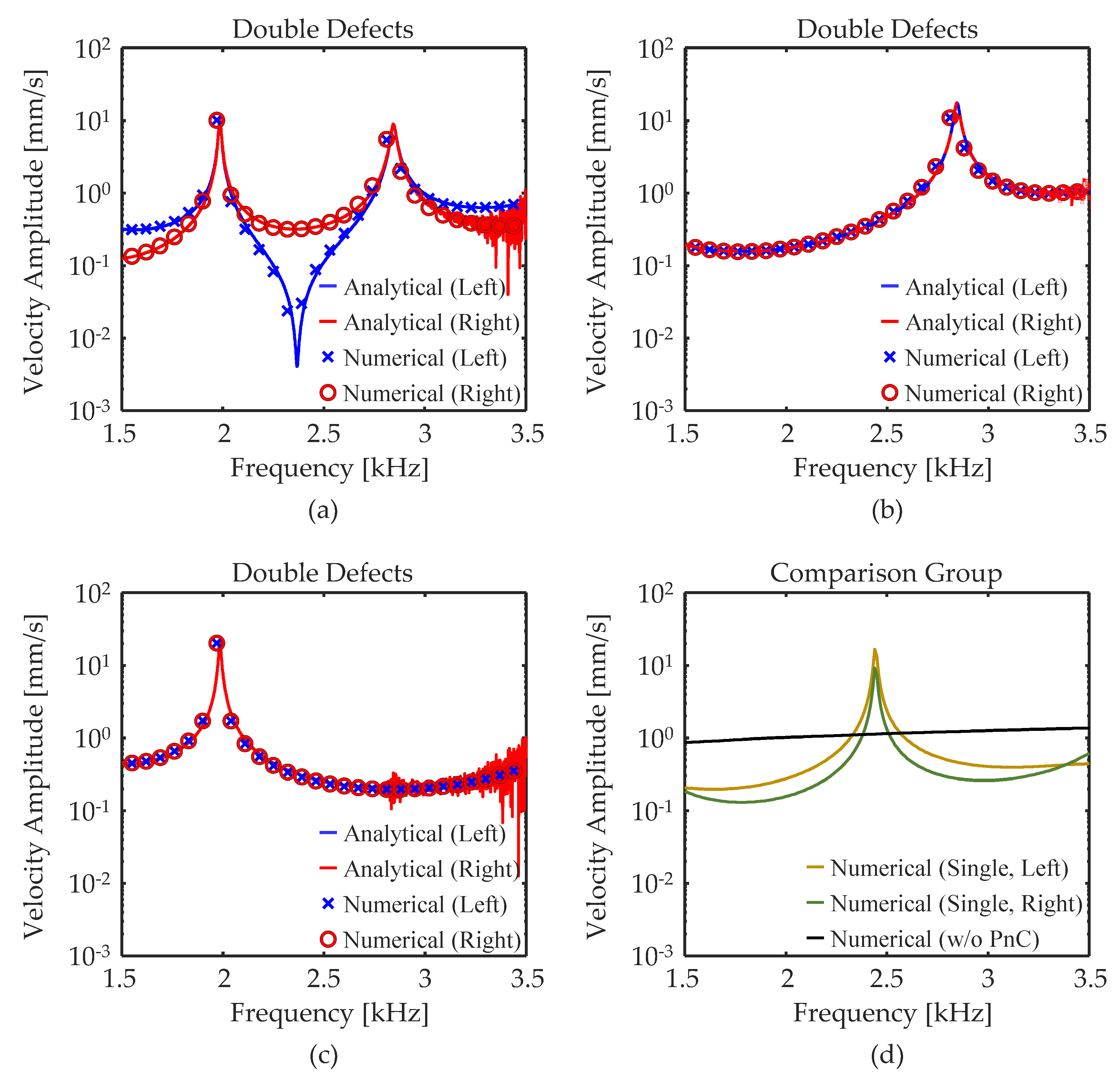
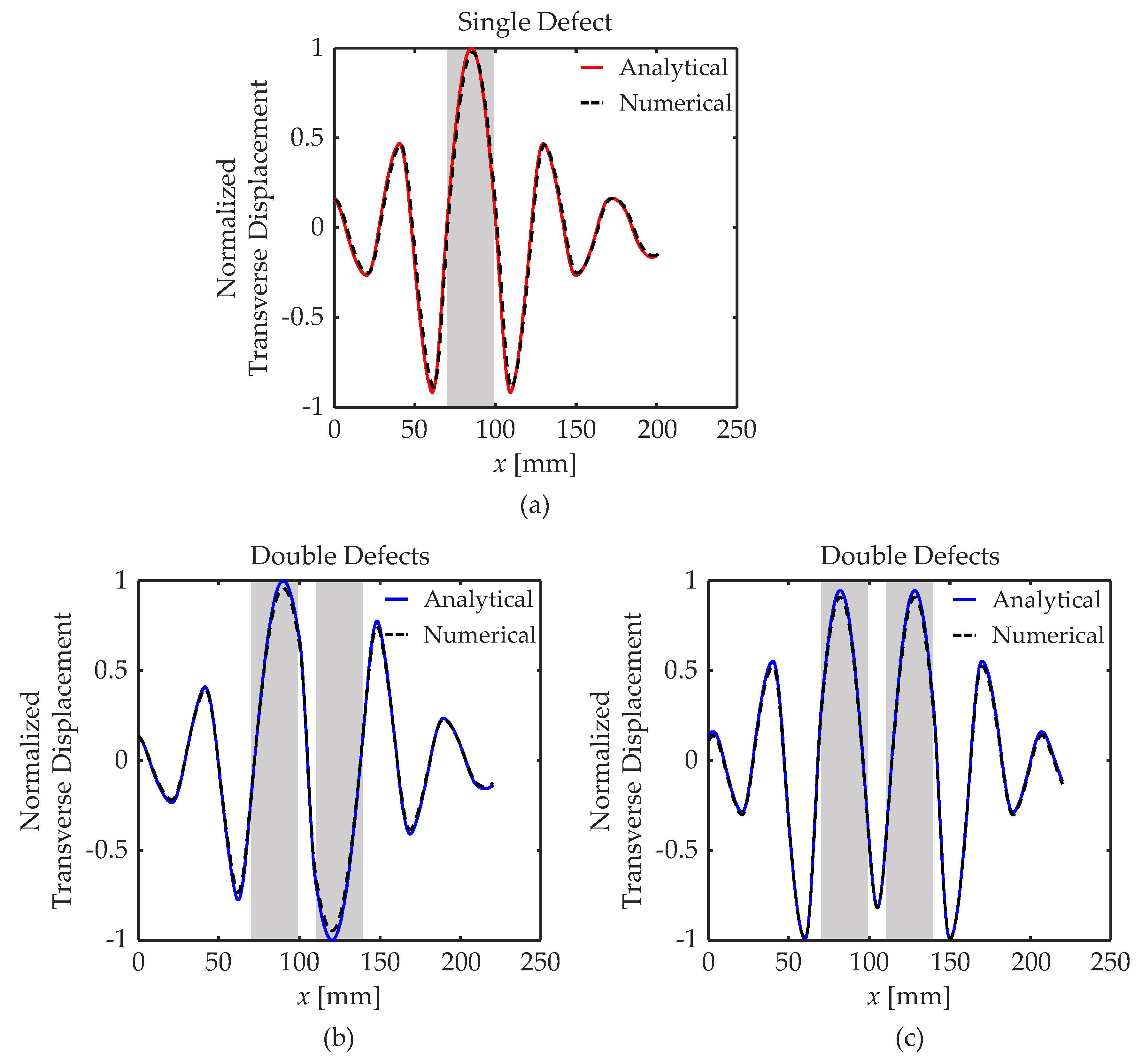
4.3. Validation Results in Wave-Excitation Analysis

In this section, our focus turns to exploring four distinct input voltage configurations: (vPD1(ω), vPD2(ω)) = (1 V, 0 V), (1 V, 1 V), and (1 V, −1 V). Visual representations in Figure 4a–c offer a glimpse into the frequency response functions (FRFs), displaying transverse velocity amplitudes of propagating waves outside the PnC with double piezoelectric defects for each setting. In addition, the velocity–amplitude FRFs of two comparison groups are plotted in Figure 4d. The outcomes of our study firmly establish that the results emanating from our analytical approach align well with those extracted through the numerical approach. Moreover, the analytical approach delivers each figure in under 2 s, whereas the finite element method necessitates a significant time investment of 18 min. Both models share an identical frequency spacing of 10 Hz from 1.5 kHz to 3.5 kHz, yet to ensure a lucid comparative assessment, we opt to present fewer dotted plots. This underscores the remarkable prowess of the highly predictive analytical approach, significantly truncating the computational time in wave-excitation analysis.
An important query may arise as to why the outcome for the scenario where (vPD1(ω), vPD2(ω)) = (0 V, 1 V) is omitted. In comparison to the findings depicted in Figure 4a encompassing the situation of (vPD1(ω), vPD2(ω)) = (1 V, 0 V), any modifications will be confined solely to the color representation. The plots illustrating the FRFs for transverse velocity amplitude will remain invariant. This intriguing observation comes from the fact that the perspective of observing the defective PnC from the front (rear) for the configuration of (vPD1(ω), vPD2(ω)) = (0 V, 1 V) aligns precisely with its rear (front) view for the configuration of (vPD1(ω), vPD2(ω)) = (1 V, 0 V). Certainly, these aforementioned characteristics have already been corroborated in a prior reference [25], which comprehensively explores the excitation of longitudinal waves through a PnC featuring double piezoelectric defects.
Examination of Figure 4a reveals some noteworthy observations. First, a discernable occurrence emerges in the form of two prominent peak frequencies, specifically 1.98 kHz and 2.84 kHz for the analytical approach and 1.97 kHz and 2.81 kHz for the numerical approach. Strikingly, these peak frequencies align seamlessly with the defect-band frequencies outlined in Figure 2 and Figure 3. Such alignment provides an unequivocal underpinning of the pivotal role played by the defect modes in elevating the wave-excitation efficacy. Second, a comparative assessment against the scenario devoid of the PnC, as depicted in Figure 4d, imparts a remarkable amplification factor—10.7-fold at 1.98 kHz and 7.2-fold at 2.84 kHz. Additionally, deviating from the single-defect scenario, the utilization of double defects affords a distinct advantage: it functions as an ultrasonic actuator across two frequencies. Third, it is imperative to underscore that despite the symmetrical structural arrangement, discernible distinctions manifest in the overall velocity-amplitude FRFs exhibited by the left and right semi-infinite beams. This discrepancy arises due to the asymmetry in the input voltage settings corresponding to the external mechanical load. Last, a point of intrigue arises from the synchronization observed in the velocity amplitudes at each of the peak frequencies. This coherence serves as evidence of the double-defect modes visualized in Figure 3b,c. A parallel analogy can be drawn to vibration engineering. In this context, the resonance frequency, under forced vibrations, reflects the oscillating motions inherent in a normal mode operating at a natural frequency under free vibrations.
In contrast, Figure 3b,c introduce two distinct features that deviate from the observations presented in Figure 3a. First, a significant insight pertains to the alignment of the overall velocity-amplitude FRFs observed within each respective host beam. This alignment stems from the inherent point or line symmetry exhibited in both the structural and electrical configurations. This symmetrical attribute, which governs both mechanical and electrical aspects, serves as the foundational premise for the subsequent analysis. Second, each FRF reveals the presence of one single peak—2.84 kHz in Figure 4b and 1.98 kHz in Figure 4c. This observation is accentuated by a noteworthy finding: the velocity amplitude at each respective peak frequency undergoes a twofold amplification—21.4 times in Figure 4b and 14.4 times in Figure 4c. This intriguing phenomenon can be elucidated through an understanding of the sign characteristics exhibited by the piezoelectric-effect-induced and defect-mode-induced strain fields. Notably, the frequencies of 1.98 kHz and 2.84 kHz, emblematic of the point- and line-symmetric behaviors engendered by the double defects in Figure 3b,c, respectively, play a pivotal role in this context. The input setting of (vPD1, vPD2) = (1 V, 1 V) establishes an equivalence in the strain fields exhibited by the piezoelectric defects. However, a pivotal distinction arises in the context of the defect-mode shape at 1.98 kHz (Figure 3b)—it manifests dissimilar strain fields within each defect, characterized by opposing signs. This discrepancy in strain signs leads to the inability of the defect mode to be excited at 1.98 kHz. A similar scenario unfolds regarding the absence of generation of the line-symmetric defect-mode shape at 2.84 kHz (Figure 3c) within the input setting of (vPD1, vPD2) = (1 V, −1 V). It is pertinent to dispel potential confusion: the non-generation of defect modes does not result from the destructive interference of bending waves emanating from each piezoelectric defect. Instead, it emanates from the inherent non-induction of the defect modes themselves. In summation, given the pronounced engineering implications, PnCs with double piezoelectric defects manifest the capability to discerningly determine a solitary peak frequency contingent on the input voltage configuration, thereby diverging from the single-defect scenario. This characteristic acquires enhanced prominence as the design framework of PnC-based ultrasonic actuators expands to encompass multiple defects.
Please note that, as the frequency increases, the predictive capability of the analytical approach model becomes unstable. In simpler terms, the velocity amplitude tends to fluctuate with different frequencies. According to the Euler–Bernoulli beam theory, there is a consistent increase in wavenumber as the frequency rises, as found in Equations (A7) and (A9). The Euler–Bernoulli beam theory demonstrates a consistent rise in wavenumber in reaction to increasing frequency. Additionally, the displacement field solutions in Equations (A6) and (A8) always involve unchanged hyperbolic and trigonometric functions, regardless of frequency changes. The presence of these hyperbolic characteristics, combined with significant wavenumbers, leads to unstable matrix operations. As a result, the velocity-amplitude values become unreliable beyond a specific frequency threshold. This is where the disadvantage of the analytical model based on Euler–Bernoulli beam theory becomes evident. To tackle this issue, it is recommended to explore the Timoshenko beam theory as an alternative approach and utilize additional mathematical techniques for alleviating the instability.

5. Conclusions

This undertaking establishes a significant connection, bridging a phononic crystal (PnC) with double defects and an ultrasonic actuator designed to excite bending waves. We developed an analytical approach based on the Euler–Bernoulli beam theory to predict various aspects like defect bands, defect-mode shapes, and velocity amplitudes of the excited bending waves. In evaluating the foresight offered by our analytical approach, this study confirmed that the outcomes projected by our model closely aligned with results obtained through a finite-element-method analysis. The disparity between numerical and analytical representations remained well below 1%. It is important to recognize, however, that the unwavering accuracy of this analytical model is not universally guaranteed due to its reliance on foundational modeling assumptions. Rather than aiming for absolute precision, our objective is to provide an initial framework for approximate predictions and guiding principles when designing ultrasonic actuators incorporating defective PnCs. The analytical approach serves as a preliminary means to offer predictive insights and guidelines, setting the stage for more intricate numerical techniques in the future. One notable advantage of our proposed method is its ability to significantly reduce computational resources, making it an attractive choice for preliminary design considerations.
Further investigations are suggested to enhance and build upon the findings presented in this study. The following directions for future exploration are put forward. First, a primary focus should be on refining the designs of finite-sized ultrasonic actuators. This involves a meticulous design optimization process aimed at maximizing the velocity amplitude at specific frequencies. Second, another promising avenue for expansion is to consider scenarios with multiple piezoelectric defects. This extended design approach has the potential to capture multiple peak-frequency values or widen the available frequency spectrum of ultrasonic actuators, akin to the principles applied in broadband energy harvesting. Last, the utilization of defective PnCs with an elastic foundation offers the dual benefits of reducing and environment-adaptively adjusting defect-band frequencies. These unique attributes have the potential to significantly broaden the scope of applications for ultrasonic actuators within various industries.

Author Contributions

Conceptualization, S.-H.J. and D.L.; methodology, S.-H.J. and D.L.; software, S.-H.J.; validation, D.L.; formal analysis, S.-H.J.; investigation, D.L.; writing—original draft preparation, S.-H.J.; writing—review and editing, S.-H.J.; visualization, D.L.; supervision, B.D.Y.; project administration, S.-H.J. and B.D.Y.; funding acquisition, S.-H.J. and B.D.Y. All authors have read and agreed to the published version of the manuscript.

Funding

This work was supported in part by the National Research Foundation of Korea (NRF), funded by the Ministry of Education under Grant 2022R1I1A1A01056406 and funded by the Korea Government (Ministry of Science and ICT) under Grant 2021R1A4A2001824 and 2020R1A2C3003644, and in part by the Dongguk University Research Fund of 2023.

Data Availability Statement

Not applicable.

Conflicts of Interest

The authors declare no conflict of interest.

Appendix A

Modeling Setting and Assumption

This appendix provides a basic understanding for Section 3.1 and Section 3.2. Beginning with one piezoelectric defect, its transverse motion is governed by Newton’s second law, and its governing equation becomes:
w PnC ρ D h PnC + 2 ρ P h P 2 u a x a , t t 2 = 2 m a x a , t x a 2 ,
where the subscript ‘a’ belongs to the set {PD1, PD2} [32]. In the context of bending waves and under the assumption of the small deformation theory, the internal bending moment ma(xa, t) can be expressed using the linear constitutive equation and the displacement–strain relationship for the metals and piezoelectric materials in terms of the transverse displacement ua(xa, t) [45,46]:
m a x a ,   t = w PnC h PnC / 2 h PnC / 2 z D 2 Y D 2 u a x a , t x a 2 d z D + h PnC / 2 h P h PnC / 2 z P 2 c 11 E 2 u a x a , t x a 2 + sgn z P z P e 31 E P x a , z P , t d z P + h PnC / 2 h PnC / 2 + h P z P 2 c 11 E 2 u a x a , t x a 2 + sgn z P z P e 31 E P x a , z P , t d z P .
Here, ‘sgn(z)’ stands for the sign of z. For sufficiently thin piezoelectric elements, it is assumed that the electric field becomes uniform within its internal domain. Through a series connection, the difference in electric potentials between the uppermost surface of the top element and the lowermost surface of the bottom element is aligned with an input voltage. Hence, the formulation of the electric field ‘EP(xPD, zP, t)’ is given by:
E P x a , z P , t = v t 2 h P H x a H x a l PD .
We denote the Heaviside step function as ‘H(x)’, and utilize it to define the spatial region associated with each piezoelectric element, represented by ‘H(xa) − H(xalPD).’ Prior research on piezoelectric effects has widely adopted such mathematical approaches to ensure the inclusion of piezoelectricity-related terms during spatial differential processes. Indeed, some analytical models, particularly those addressing longitudinal waves and transverse vibrations, have appealed remarkable agreement with finite-element-method results [25,26,47,48].
By substituting Equations (A2) and (A3) into Equation (A1), the governing equation is thus reformulated as follows:
ρ S PD 2 u a x a , t t 2 + YI PD 4 u a x a , t x a 4 = κ P v t d δ x a d x a d δ x a l PD d x a ,
where ‘δ(x)’ is the Dirac delta function. For one piezoelectric defect, the terms ‘(ρS)PD’ and ‘(YI)PD’ represent the homogenized mass per unit length and bending stiffness, respectively. The term ‘κP’ quantifies the degree of electroelastic coupling of the series-connected bimorph piezoelectric elements. To summarize, these physical quantities can be described as follows:
ρ S PD = w PnC ρ D h PnC + 2 ρ P h P , YI PD = w PnC Y D h PnC 3 12 + 2 c 11 E 3 h PnC + 2 h P 2 3 h PnC 2 3 , κ P = w PnC e 31 h PnC + h P 2 .
When the wave-excitation system is subjected to time-harmonic motions such that ‘u(x, t) = u(x)exp(−jωt)’, the displacement solution to Equation (A4) can be divided into two groups: homogeneous and nonhomogeneous solutions. A typical homogeneous solution ‘ua,H(xa, ω)’ to Equation (A4) comprises a linear combination of the hyperbolic and trigonometric functions. A nonhomogeneous solution ‘ua,NH(xa, ω)’ to Equation (A4) can be expressed using Green’s function [49,50]. Equation (A4) represents the introduction of two spatially concentrated bending moments in the opposite direction but with the same magnitude as κPv(ω). Consequently, the total transverse displacement field ‘ua(xa, ω)’ within one piezoelectric defect can be expressed as:
u a x a , ω = u a , H x a , ω + v a ω u a , NH x a , ω u a , H x a , ω = P a , HY ω exp k PD ω x a + Q a , HY ω exp k PD ω x a + P a , TR ω exp j k PD ω x a + Q PD , TR ω exp j k PD ω x a u a , NH x a , ω = κ P 4 YI PD k PD 2 ω exp k PD ω x a + exp k PD ω x a + l PD exp j k PD ω x a + exp j k PD ω x a + l PD ,
where the wavenumber kPD(ω) used in the Euler–Bernoulli beam theory is [51]:
k PD ω = ρ S PD ω 2 YI PD 4 .
The subscripts ‘HY’ and ‘TR’ are indeed short forms for the hyperbolic function and trigonometric function, respectively.
In order to determine the transverse displacement of remaining beams without the piezoelectric elements, the simple removal of the terms associated with the piezoelectric elements is performed. The mechanical domain effects are disregarded by setting the height of the piezoelectric elements to zero. Moreover, the electrical domain effects are naturally eliminated due to the zero value of the piezoelectric coupling coefficient. As a result, the expression for the transverse displacement field of these beams takes the same form as the homogenous solution in Equation (A6) as follows:
u b x b , ω = P b , HY ω exp k b ω x b + Q b , HY ω exp k b ω x b + P b , TR ω exp j k b ω x b + Q b , TR ω exp j k b ω x b ,
where the subscript ‘b’ belongs to the set {DU, LU, LS, RS}. The spatial positions are defined as follows: xDU ∈ (0, lDU), xLU ∈ (0, lLU), xLS ∈ (−, 0), and xRS ∈ (0, ). The wavenumber kb(ω) used in the Euler–Bernoulli beam theory is [51]:
k b ω = ρ b S PnC ω 2 Y b I PnC 4 .
To progress with the analysis, it becomes crucial to characterize the frequency-dependent transverse displacement coefficients PHY(ω), QHY(ω), PTR(ω), and QTR(ω) in Equations (A6) and (A8). Section 3.1 and Section 3.2 concentrate on the dispersion and wave-excitation analyses, respectively. Using the transfer-matrix and S-parameter methods, we determine the four displacement coefficients for each beam and describe in detail how to compute desired outputs.

Appendix B

Comsol Setting

In line with established practices within the domain of analytical and semi-analytical models, a validation process is implemented to assess both the significance of the PnC with piezoelectric double defects for ultrasonic actuators and the efficacy of the enhanced model. To facilitate this investigation, the widely recognized software Comsol Multiphysics 6.1 is employed. Comsol Multiphysics is extensively utilized for predictive analysis in elastic wave propagation systems [52,53] and configurations incorporating intelligent materials [54,55]. The key configuration parameters utilized within the software are as follows: the analyses are conducted within a two-dimensional spatial domain under the plane-stress condition. Dispersion analysis in Figure A1a is carried out using the ‘Eigenfrequency’ solver in the ‘Solid Mechanics’ physics, augmented by the ‘Periodic Condition’ feature. Shifting to the ‘Frequency Domain’ solver, simultaneous operation of the ‘Solid Mechanics’ and ‘Electrostatics’ physics, along with the ‘Multiphysics (Piezoelectric Effects)’, facilitates the analysis of wave excitation in Figure A1b. To emulate semi-infinite conditions on both sides of the bending-wave-excitation system, a ‘Perfectly Matched Layer’ setting is applied to the domains outside the defective PnC. Displacement fields and electric potential are discretized using quadratic serendipity. The mesh size, established through convergence testing, is set at one tenth of the lattice constant. For a comprehensive grasp of the intricate Comsol settings, a valuable reference, available in Refs. [25,26,27], can provide deeper insights and understanding.
Figure A1. Basic settings of Comsol Multiphysics 6.1 in (a) dispersion analysis and (b) wave-excitation analysis.
Mathematics 11 03852 g0a1

References

  1. Kennedy, J.; Lim, C. Machine learning and deep learning in phononic crystals and metamaterials: A review. Mater. Today Commun. 2022, 33, 104606. [Google Scholar]
  2. Muhammad; Lim, C. From photonic crystals to seismic metamaterials: A review via phononic crystals and acoustic metamaterials. Arch. Comput. Methods Eng. 2022, 29, 1137–1198. [Google Scholar] [CrossRef]
  3. Jo, S.-H.; Yoon, H.; Shin, Y.C.; Youn, B.D. Revealing defect-mode-enabled energy localization mechanisms of a one-dimensional phononic crystal. Int. J. Mech. Sci. 2022, 215, 106950. [Google Scholar] [CrossRef]
  4. Geng, Q.; Fong, P.-K.; Ning, J.; Shao, Z.; Li, Y. Thermally-induced transitions of multi-frequency defect wave localization and energy harvesting of phononic crystal plate. Int. J. Mech. Sci. 2022, 222, 107253. [Google Scholar] [CrossRef]
  5. Park, S.; Jeon, W. Ultra-wide low-frequency band gap in a tapered phononic beam. J. Sound Vib. 2021, 499, 115977. [Google Scholar] [CrossRef]
  6. Sun, Y.; Yu, Y.; Zuo, Y.; Qiu, L.; Dong, M.; Ye, J.; Yang, J. Band gap and experimental study in phononic crystals with super-cell structure. Results Phys. 2019, 13, 102200. [Google Scholar] [CrossRef]
  7. He, Z.; Zhang, G.; Chen, X.; Cong, Y.; Gu, S.; Hong, J. Elastic wave harvesting in piezoelectric-defect-introduced phononic crystal microplates. Int. J. Mech. Sci. 2023, 239, 107892. [Google Scholar] [CrossRef]
  8. Reetz, C.; Fischer, R.; Assumpcao, G.G.; McNally, D.P.; Burns, P.S.; Sankey, J.C.; Regal, C.A. Analysis of membrane phononic crystals with wide band gaps and low-mass defects. Phys. Rev. Appl. 2019, 12, 044027. [Google Scholar] [CrossRef]
  9. Wu, F.; Liu, Z.; Liu, Y. Splitting and tuning characteristics of the point defect modes in two-dimensional phononic crystals. Phys. Rev. E 2004, 69, 066609. [Google Scholar] [CrossRef]
  10. Aly, A.H.; Mehaney, A. Phononic crystals with one-dimensional defect as sensor materials. Indian J. Phys. 2017, 91, 1021–1028. [Google Scholar] [CrossRef]
  11. Jo, S.-H.; Shin, Y.C.; Choi, W.; Yoon, H.; Youn, B.D.; Kim, M. Double defects-induced elastic wave coupling and energy localization in a phononic crystal. Nano Converg. 2021, 8, 27. [Google Scholar] [CrossRef] [PubMed]
  12. Geng, Q.; Wang, T.; Wu, L.; Li, Y. Defect coupling behavior and flexural wave energy harvesting of phononic crystal beams with double defects in thermal environments. J. Phys. D Appl. Phys. 2021, 54, 225501. [Google Scholar] [CrossRef]
  13. Habib, M.; Lantgios, I.; Hornbostel, K. A review of ceramic, polymer and composite piezoelectric materials. J. Phys. D Appl. Phys. 2022, 55, 423002. [Google Scholar] [CrossRef]
  14. Chen, L.; Liu, H.; Qi, H.; Chen, J. High-electromechanical performance for high-power piezoelectric applications: Fundamental, progress, and perspective. Prog. Mater. Sci. 2022, 127, 100944. [Google Scholar] [CrossRef]
  15. Thomes, R.L.; Beli, D.; Sugino, C.; Erturk, A.; Junior, C.D.M. Programmable moving defect for spatiotemporal wave localization in piezoelectric metamaterials. Phys. Rev. Appl. 2023, 19, 064031. [Google Scholar] [CrossRef]
  16. Thomes, R.L.; Beli, D.; Junior, C.D.M. Space–time wave localization in electromechanical metamaterial beams with programmable defects. Mech. Syst. Signal Process. 2022, 167, 108550. [Google Scholar] [CrossRef]
  17. Jo, S.-H.; Youn, B.D. An explicit solution for the design of a target-frequency-customized, piezoelectric-defect-introduced phononic crystal for elastic wave energy harvesting. J. Appl. Phys. 2021, 130, 184902. [Google Scholar] [CrossRef]
  18. Jo, S.-H.; Youn, B.D. An improved analytical model that considers lateral effects of a phononic crystal with a piezoelectric defect for elastic wave energy harvesting. Int. J. Mech. Sci. 2021, 205, 106593. [Google Scholar] [CrossRef]
  19. Lee, G.; Park, J.; Choi, W.; Ji, B.; Kim, M.; Rho, J. Multiband elastic wave energy localization for highly amplified piezoelectric energy harvesting using trampoline metamaterials. Mech. Syst. Signal Process. 2023, 200, 110593. [Google Scholar] [CrossRef]
  20. Park, H.W.; Seung, H.M.; Choi, W.; Kim, M.; Oh, J.H. Highly tunable low frequency metamaterial cavity for vibration localization. Sci. Rep. 2022, 12, 9714. [Google Scholar] [CrossRef]
  21. Aly, A.H.; Nagaty, A.; Mehaney, A. One-dimensional phononic crystals that incorporate a defective piezoelectric/piezomagnetic as a new sensor. Eur. Phys. J. B 2018, 91, 211. [Google Scholar] [CrossRef]
  22. Aly, A.H.; Nagaty, A.; Mehaney, A. Thermal properties of one-dimensional piezoelectric phononic crystal. Eur. Phys. J. B 2018, 91, 251. [Google Scholar] [CrossRef]
  23. Jin, H.; Gao, X.; Ren, K.; Liu, J.; Qiao, L.; Liu, M.; Chen, W.; He, Y.; Dong, S.; Xu, Z. Review on piezoelectric actuators based on high-performance piezoelectric materials. IEEE Trans. Ultrason. Ferroelectr. Freq. Control 2022, 69, 3057–3069. [Google Scholar] [CrossRef] [PubMed]
  24. Aabid, A.; Hrairi, M.; Mohamed Ali, S.J.; Ibrahim, Y.E. Review of piezoelectric actuator applications in damaged structures: Challenges and opportunities. ACS Omega 2023, 8, 2844–2860. [Google Scholar] [CrossRef] [PubMed]
  25. Jo, S.-H.; Lee, D.; Yoon, H.; Youn, B.D. Double piezoelectric defects in phononic crystals for ultrasonic transducers. J. Phys. D Appl. Phys. 2023, 56, 74002. [Google Scholar] [CrossRef]
  26. Jo, S.-H.; Youn, B.D. Enhanced ultrasonic wave generation using energy-localized behaviors of phononic crystals. Int. J. Mech. Sci. 2022, 228, 107483. [Google Scholar] [CrossRef]
  27. Jo, S.; Lee, D. Flexural-wave-generation using a phononic crystal with a piezoelectric defect. Appl. Math. Mech. 2023, 44, 1241–1262. [Google Scholar] [CrossRef]
  28. Grover, S.; Moddel, G. Engineering the current–voltage characteristics of metal–insulator–metal diodes using double-insulator tunnel barriers. Solid-State Electron. 2012, 67, 94–99. [Google Scholar] [CrossRef]
  29. Haynes, M.; Moghaddam, M. Multipole and S-parameter antenna and propagation model. IEEE Trans. Antennas Propag. 2010, 59, 225–235. [Google Scholar] [CrossRef]
  30. Ali, A.; Pasha, R.A.; Elahi, H.; Sheeraz, M.A.; Bibi, S.; Hassan, Z.U.; Eugeni, M.; Gaudenzi, P. Investigation of deformation in bimorph piezoelectric actuator: Analytical, numerical and experimental approach. Integr. Ferroelectr. 2019, 201, 94–109. [Google Scholar] [CrossRef]
  31. Asadi Dereshgi, H.; Dal, H.; Sayan, M.E. Analytical analysis of a circular unimorph piezoelectric actuator in the range of low voltages and pressures. Microsyst. Technol. 2020, 26, 2453–2464. [Google Scholar] [CrossRef]
  32. Erturk, A.; Inman, D.J. An experimentally validated bimorph cantilever model for piezoelectric energy harvesting from base excitations. Smart Mater. Struct. 2009, 18, 025009. [Google Scholar] [CrossRef]
  33. Gao, X.; Yang, J.; Wu, J.; Xin, X.; Li, Z.; Yuan, X.; Shen, X.; Dong, S. Piezoelectric actuators and motors: Materials, designs, and applications. Adv. Mater. Technol. 2020, 5, 1900716. [Google Scholar] [CrossRef]
  34. Zhang, S.; Liu, Y.; Deng, J.; Tian, X.; Gao, X. Development of a two-DOF inertial rotary motor using a piezoelectric actuator constructed on four bimorphs. Mech. Syst. Signal Process. 2021, 149, 107213. [Google Scholar] [CrossRef]
  35. Zhou, W.; Lim, C. Topological edge modeling and localization of protected interface modes in 1D phononic crystals for longitudinal and bending elastic waves. Int. J. Mech. Sci. 2019, 159, 359–372. [Google Scholar]
  36. Liang, X.; Wang, T.; Jiang, X.; Liu, Z.; Ruan, Y.; Deng, Y. A numerical method for flexural vibration band gaps in a phononic crystal beam with locally resonant oscillators. Crystals 2019, 9, 293. [Google Scholar] [CrossRef]
  37. Guo, Y.; Li, L.; Chuang, K.-C. Analysis of bending waves in phononic crystal beams with defects. Crystals 2018, 8, 21. [Google Scholar] [CrossRef]
  38. Han, L.; Zhang, Y.; Ni, Z.-Q.; Zhang, Z.-M.; Jiang, L.-H. A modified transfer matrix method for the study of the bending vibration band structure in phononic crystal Euler beams. Phys. B Condens. Matter 2012, 407, 4579–4583. [Google Scholar] [CrossRef]
  39. Yu, P.; Wang, L.; Zhang, S.; Jin, J. Transfer matrix modeling and experimental verification of forked piezoelectric actuators. Int. J. Mech. Sci. 2022, 232, 107604. [Google Scholar] [CrossRef]
  40. Boiangiu, M.; Ceausu, V.; Untaroiu, C.D. A transfer matrix method for free vibration analysis of Euler-Bernoulli beams with variable cross section. J. Vib. Control 2016, 22, 2591–2602. [Google Scholar] [CrossRef]
  41. Lee, H.J.; Lee, J.K.; Kim, Y.Y. Elastic metamaterial-based impedance-varying phononic bandgap structures for bandpass filters. J. Sound Vib. 2015, 353, 58–74. [Google Scholar] [CrossRef]
  42. Lucklum, R.; Ke, M.; Zubtsov, M. Two-dimensional phononic crystal sensor based on a cavity mode. Sens. Actuators B Chem. 2012, 171, 271–277. [Google Scholar] [CrossRef]
  43. Lee, H.J.; Lee, H.S.; Ma, P.S.; Kim, Y.Y. Effective material parameter retrieval of anisotropic elastic metamaterials with inherent nonlocality. J. Appl. Phys. 2016, 120, 104902. [Google Scholar] [CrossRef]
  44. Kweun, J.M.; Lee, H.J.; Oh, J.H.; Seung, H.M.; Kim, Y.Y. Transmodal Fabry-Pérot resonance: Theory and realization with elastic metamaterials. Phys. Rev. Lett. 2017, 118, 205901. [Google Scholar] [CrossRef] [PubMed]
  45. Wang, G. Analysis of bimorph piezoelectric beam energy harvesters using Timoshenko and Euler–Bernoulli beam theory. J. Intell. Mater. Syst. Struct. 2013, 24, 226–239. [Google Scholar] [CrossRef]
  46. Erturk, A. Assumed-modes modeling of piezoelectric energy harvesters: Euler–Bernoulli, Rayleigh, and Timoshenko models with axial deformations. Comput. Struct. 2012, 106, 214–227. [Google Scholar] [CrossRef]
  47. Hosseini, R.; Hamedi, M. Improvements in energy harvesting capabilities by using different shapes of piezoelectric bimorphs. J. Micromechanics Microengineering 2015, 25, 125008. [Google Scholar] [CrossRef]
  48. Abdelkefi, A.; Yan, Z.; Hajj, M.R. Modeling and nonlinear analysis of piezoelectric energy harvesting from transverse galloping. Smart Mater. Struct. 2013, 22, 025016. [Google Scholar] [CrossRef]
  49. Ghannadiasl, A.; Ajirlou, S.K. Forced vibration of multi-span cracked Euler–Bernoulli beams using dynamic Green function formulation. Appl. Acoust. 2019, 148, 484–494. [Google Scholar] [CrossRef]
  50. Mazilu, T. Numerically stable form of Green’s function for a free-free uniform Timoshenko beam. Mathematics 2022, 11, 86. [Google Scholar] [CrossRef]
  51. Ni, Z.-Q.; Zhang, Y.; Jiang, L.-H.; Han, L. Bending vibration band structure of phononic crystal beam by modified transfer matrix method. Int. J. Mod. Phys. B 2014, 28, 1450093. [Google Scholar] [CrossRef]
  52. Kim, H.J.; Park, C.I.; Kim, K.; Kim, Y.Y. Meta-ring for enhancing emission efficiency of omnidirectional SH waves. Int. J. Mech. Sci. 2023, 251, 108354. [Google Scholar] [CrossRef]
  53. Kim, S.Y.; Oh, Y.B.; Lee, J.S.; Kim, Y.Y. Anomalous mode-converting reflection of elastic waves using strip-type metagratings. Mech. Syst. Signal Process. 2023, 186, 109867. [Google Scholar] [CrossRef]
  54. Hosseinkhani, A.; Ebrahimian, F.; Younesian, D.; Moayedizadeh, A. Defected meta-lattice structures for the enhanced localized vibrational energy harvesting. Nano Energy 2022, 100, 107488. [Google Scholar] [CrossRef]
  55. Shao, H.; Chen, G.; He, H. Elastic wave localization and energy harvesting defined by piezoelectric patches on phononic crystal waveguide. Phys. Lett. A 2021, 403, 127366. [Google Scholar] [CrossRef]
Figure 1. A schematic portrayal of an advanced ultrasonic actuator concept that leverages a PnC with double piezoelectric defects for bending-wave excitation.
Mathematics 11 03852 g001
Figure 2. Results in dispersion curves, involving one band gap at the unit-cell level, one defect band at the single-defect-introduced PnC level, and two defect bands at the double-defect-introduced PnC level.
Mathematics 11 03852 g002
Figure 3. Results in defect-mode shapes: (a) the single-defect modes at 2.45 kHz (analytical approach) and 2.44 kHz (numerical approach), (b) the point-symmetric double-defect modes at 1.98 kHz (analytical approach) and 1.97 kHz (numerical approach), and (c) the line-symmetric double-defect modes at 2.84 kHz (analytical approach) and 2.81 kHz (numerical approach). The gray-shaded area presents the domain of the piezoelectric defects.
Mathematics 11 03852 g003
Figure 4. Results in velocity–amplitude FRFs in the case of (a) (vPD1(ω), vPD2(ω)) = (1 V, 0 V), (b) (vPD1(ω), vPD2(ω)) = (1 V, 1 V), (c) (vPD1(ω), vPD2(ω)) = (1 V, −1 V), and (d) a PnC with a single piezoelectric defect and infinite beam with bimorph piezoelectric elements in the absence of the defective PnC. (ac) Present the results in the case of double defects; the terms ‘Left’ and ‘Right’ refer to the left-sided and right-sided semi-infinite structures. (d) Shows the results in the case of a single defect and in the absence of the PnC.
Mathematics 11 03852 g004
Disclaimer/Publisher’s Note: The statements, opinions and data contained in all publications are solely those of the individual author(s) and contributor(s) and not of MDPI and/or the editor(s). MDPI and/or the editor(s) disclaim responsibility for any injury to people or property resulting from any ideas, methods, instructions or products referred to in the content.

