Article

Continuous-Control-Set Model Predictive Control for Three-Level DC–DC Converter with Unbalanced Loads in Bipolar Electric Vehicle Charging Stations

1
Department of Electrical Engineering, National Kaohsiung University of Science and Technology, Kaohsiung City 807618, Taiwan
2
Department of Electronics and Electrical Engineering, Technical University of Catalonia, 08800 Villanova, Spain
3
Center for Research on Microgrids, Department of Energy Technology, Aalborg University, 9220 Aalborg, Denmark
4
Department of Mathematical Methods and Operations Research, University of Zilina, Univerzitna 8215/1, SK-01026 Zilina, Slovakia
5
Electrical Engineering Department, Faculty of Engineering at Shoubra, Benha University, Cairo 11629, Egypt
*
Authors to whom correspondence should be addressed.
Mathematics 2022, 10(19), 3444; https://doi.org/10.3390/math10193444
Submission received: 22 August 2022 / Revised: 14 September 2022 / Accepted: 19 September 2022 / Published: 22 September 2022
(This article belongs to the Special Issue Model Predictive Control and Optimization for Cyber-Physical Systems)

Abstract

:
Zero-emission transportation is currently a public priority, especially in big cities. For this reason, the use of electric vehicles (EVs) is receiving much attention. To facilitate the adoption of EVs, a proper charging infrastructure together with energy management is essential. This article proposes a design guideline for a direct current (DC) charging station with bipolar properties. A bipolar system can convert a two-wire system into three wires in a microgrid system with a neutral line. The configuration of the bipolar system supports different loads; therefore, the unbalanced operation is inherent to the system. The proposed bipolar DC charging station (CS) has a three-level balancing converter that reduces the step-down effort chargers. Moreover, this paper proposes the continuous-control-set model predictive control (CCS-MPC)-based balancing strategy that allows the handling of different output loads while keeping the neutral-line voltage efficiently regulated with improved dynamic performance compared to a traditional controller. Stability and parameter robustness analyses are also performed for the control parameter selection. To ensure the performance of the proposed method, both simulation and experimental results are presented and compared with those obtained from the traditional methods.
MSC:
93-08; 93B35; 93B45; 93B52; 93B53; 93B55

1. Introduction

Due to the rapidly increasing number of electric vehicles (EVs) and increased depletion of fossil fuels, the demand for renewable energy source (RES)-based EV charging stations (CSs) is also rising to alleviate the anxiety of EV drivers [1]. Surveys [2,3,4] depict that the number of available CSs, the charging time, and the range per charge are the biggest concerns of consumers, which also impact the sale of EVs. There is an urgent need to deploy fast CS infrastructure to increase the sale of EVs and reduce the charging time [5]. In addition, the development of RESs such as photovoltaic (PV), hydrogen fuel cell, and DC bus systems have made the distribution system more manageable than conventional distribution systems [6]. Compared to AC distribution systems, RES-based DC power distribution architectures have more advantages, such as fewer power conversion modes with high power-conversion efficiency and lower cost.
There are two basic topologies of fast CSs: unipolar, using two-level converters, and/or bipolar, using three-level converters [2]. The latter topology has considerable advantages compared to the unipolar type. It offers better power quality, fewer switching power losses, more flexibility to connect loads to the DC bus, and distinct DC voltage levels [7]. Moreover, the bipolar DC bus architecture is more reliable than the unipolar system as it can operate with only one DC bus (positive or negative) in case of a fault [8]. Consequently, the bipolar system is widely used in DC power systems. For example, IBM and Intel have equipped their data centers with bipolar systems. Similarly, it has also been applied in DC transmission systems such as the ±500 kV Rihand–Dadri transmission project in India, and ±800 kV Jinping Suzhou transmission project in China. However, bipolar topology has an inherent voltage imbalance issue on the positive and negative DC buses because of independent DC buses that can become visible due to stochastic EVs’ charging occurrences and their different load characteristics [2,9,10]. The stochastic nature of charging behavior affects the power quality, increases the voltage stress on power switches, increases the risk of problems with grid side currents, and makes the bipolar system unbalanced.
The aforementioned unbalancing issue can be addressed by employing bipolar DC CSs topologies suggesting to deploy neutral-point-clamped (NPC) converter with three levels of DC–DC converters [2,11]. A typical example of the voltage imbalance problem in the bipolar DC bus system by deploying NPC with three-level DC–DC converters is explored in [1]. However, the NPC converter has voltage-balancing limits, so it cannot be relied upon to balance the DC bus voltage under all operating conditions by considering the random arrival of EVs. Similarly, [6] solved the same problem by applying additional balancing circuits with an NPC converter, but it has the drawback of increased costs and poor efficiency. In [9], the bipolar DC bus was balanced using an energy storage system (ESS) with an NPC and integrated inductors. In addition, interleaved multiphase buck converters have been applied in two-level charging stations due to their voltage-matching capabilities to share high power among multiple nodes. Three-level non-isolated converters have also been widely used in high-power and high-voltage applications to decrease the voltage stress on semiconductor devices and to improve power ratings [12].
The applications of voltage balancers with conventional linear control systems are gaining more attention for developing bipolar DC microgrids [13,14,15,16]. For example, a simple dual-buck voltage balancer has been proposed and successfully applied in a DC microgrid in [14]. Likewise, the buck/boost type of voltage balancing converter topology has been used to balance the bipolar DC system [14,17] to handle high-power fast CSs for EVs. Moreover, the voltage balancer is upgraded by applying multi-level converter topologies, leading to a higher capacity with different voltage levels. All of these aforementioned studies used a linear control, while the proportional integral (PI) controller is tuned-based on the operation points, and does not have the ability to deal with the system constraints. Consequently, the system performance and transient response is reduced in the existence of external disturbance and sudden load fluctuations [18]. Alternatively, optimization algorithms such as meta-heuristics can be used to control the tuning process for DC systems, thus improving the transient response to external disturbances such as sudden load changes [19,20]. However, those optimal tuning processes are still based on the desired operation points and they are not robust to parameter uncertainties. Moreover, recent work based on neuroadaptive learning for nonlinear systems to handle a disturbance has been studied in [21]. These adaptive controllers can be trained to handle mismatch disturbances. However, those methods require high computational power, compromising the stability of high-frequency system applications. Instead, a wider bandwidth control can be accomplished by the MPC while using smaller stability measures in the tuning steps [22].
Recently, model predictive control (MPC) has been recognized as a powerful tool for controlling high-power converters. MPC is very appropriate to control power electronic systems due is its fundamental characteristics, such as high bandwidth control, faster transient response, and the ability to account in a simple way for system constraints and non-linearities [23]. In addition, the other prominent features of MPC are the robustness of the system parameter variations, design simplicity, flexibility to include system constraints, and system non-linearities. Likewise, MPC can also help to achieve multiple control objectives by utilizing cost functions [24]. Therefore, this practice has been frequently applied to control power converters such as NPC [25,26,27] active neutral-clamped converters [28], cascade half-bridge converters [29], modular multi-level converters [30,31], and flying capacitors [32] to balance and control the current and voltage.
From the perspective of power electronic converters, MPC can attain two forms: (1) finite-set model predictive control (FCS-MPC) and (2) continuous-control-set model predictive control (CCS-MPC) [24,33]. The cost function is calculated and minimized for a finite number of switching states in the case of the FCS-MPC strategy. This strategy employs a comparator as an alternative to a modulator to determine the optimal switching frequency, which increases the computational burden and some non-desirable components [24]. However, the CCS-MPC approach can help to address the issues associated with the FCS-MPC approach more conveniently, since this control strategy predicts state variables using a discrete state model of the power converters where the state-space variables can be estimated using a conventional state observer [23]. The cost function is calculated and minimized inside the prediction horizon for obtaining vectors of future control actions. According to the receding horizon control, only the first sample of the vector is used as a space vector modulator, which leads to a fixed switching frequency; therefore, it offers less computational burden. One can always refer to a detailed comparative analysis conducted in [34,35] to compare the dynamic performance and make an appropriate choice of a power converter for a given application. Owing to the increasing use of CCS-MPC in industrial applications [35], the decoupling of switching frequency from the controller sampling time helps to operate the converter at the fixed switching frequency and enhances the control flexibility. With these benefits, it is necessary to emphasize that the FCS-MPC has been studied for a bipolar DC microgrid under a variable switching frequency, which may lead to increased computational cost [36,37]. Nevertheless, the implementation of CCS-MPC has not been very well explored for bipolar DC microgrid applications. Therefore, this paper proposes an enhanced CCS-MPC-based control strategy with a half-bridge balancing converter. This method has a high utilization of DC–DC converters to reduce the energy loss and improve the utilization of the DC power supply. Consequently, the bipolar DC CS has unique benefits in cost, power supply flexibility, and security. In a bipolar DC CS, there is coupling between the positive and the negative poles. The imbalance of the output voltages from positive and negative power supplies, loads, and line resistance can cause an unbalanced current in the neutral line, resulting in voltage deviations on the bipolar DC bus from the rated value. The proposed method has demonstrated its effectiveness in controlling power converters with a faster transient response and achieves an excellent dynamic performance without the need for any stability analysis. Moreover, the proposed CCS-MPC reduces the steady-state oscillation and increases the robustness against parameter uncertainties compared to previous methods [13,14,15,16]. In addition, the involvement of a simple cost function approach helps to avoid the tedious controller design methods such as Bode plot and Nyquist analysis approaches. CCS-MPC techniques have been widely used in different systems, but their application in bipolar DC microgrids still requires further effort and attention. The proposed control strategy opens up a new research topic for implementing the CCS-MPC in bipolar DC microgrids, as the bipolar DC bus suffers from intermittent operations due to the unbalanced power distribution between the DC buses. The three-level balancing converter combined with CCS-MPC provides a higher degree of freedom to accurately control the bipolar system during sudden load changes to achieve a better voltage balance. These asymmetrical operations can cause an unbalance in the three-phase voltage that deteriorates the power quality and leads to a premature failure of semiconductor devices. The application of the CCS-MPC approach will allow excellent output voltage regulations during load fluctuations.
The key contribution of this article is the design of a CCS-MPC controller for a bipolar EV charging station with the following properties:
  • Robustness of the output voltage over sudden load changes.
  • Robustness against model parameter uncertainties.
  • A fixed switching frequency is achievable with a reduced computational burden.
  • The implementation of a CCS-MPC control scheme maintains the bipolar DC bus with better damping performance than an optimal PI controller.
  • The steady-state oscillations are reduced compared to an optimal PI controller.
The organization of this paper is as follows: the generic topological description of the proposed DC CS is introduced in Section 2. The CCS-MPC-based control scheme with stability analysis applied to the half-bridge balancing converter is described in Section 3. Subsequently, the operating modes of the balancing converter are analyzed in Section 4. The numerical results, control parameter robustness analysis, and comparison of the proposed controller with the optimal PI controller based on the genetic algorithm (GA) are carried out in Section 5. Finally, the valuable interpretations of the proposed work are summarized in Section 6.

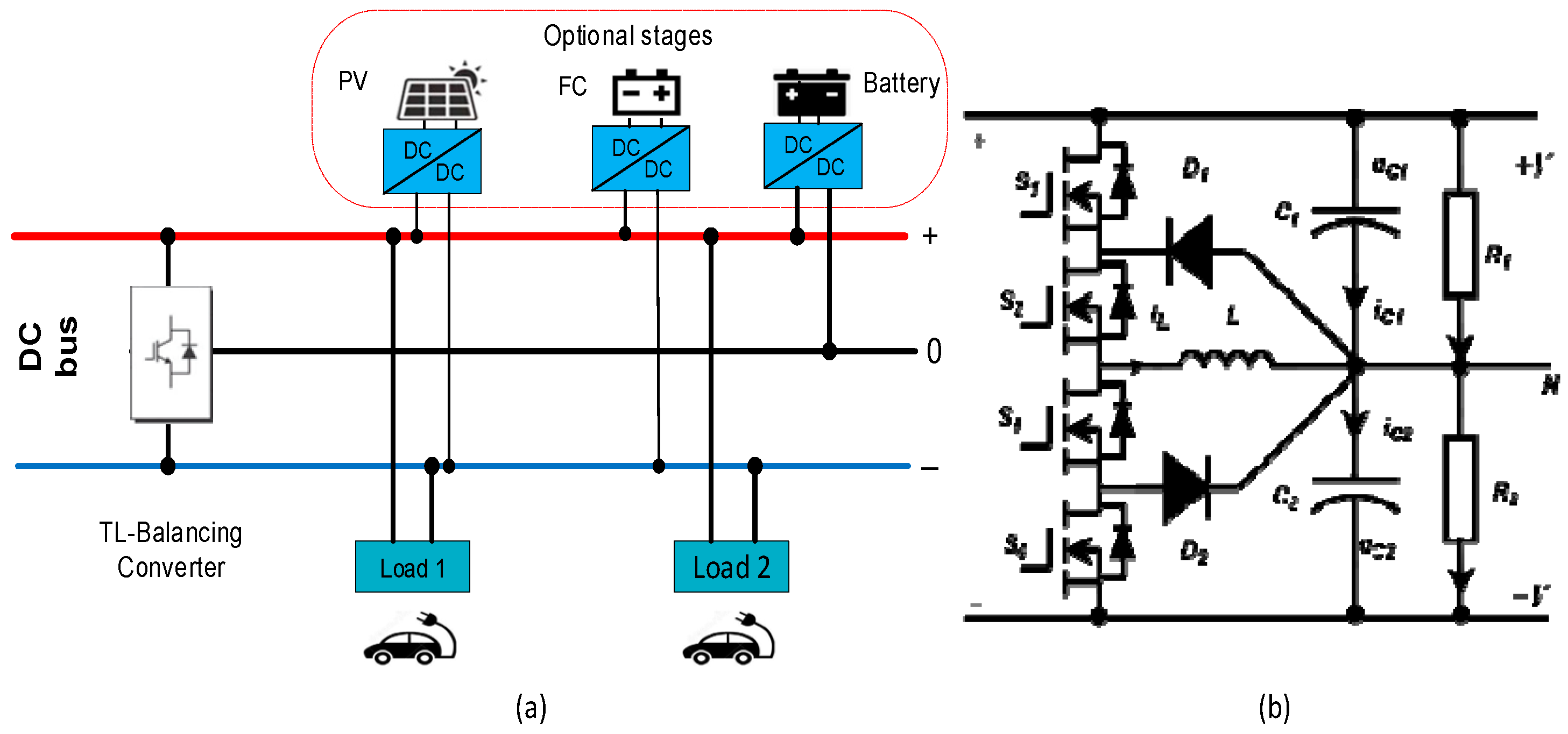
2. Topology of Bipolar DC EV Charging Station

The topology of the proposed bipolar CS architecture is exemplified in Figure 1, where a three-level balancing DC–DC converter (see Figure 1b) is employed and controlled using the CCS-MPC strategy to make this system bipolar to achieve better DC bus voltage/current regulation. The bipolar structure allows the connection of distributed power sources such as RESs (PV, wind, and fuel cell) and energy storage systems [9,38]. Conventional DC–DC converters are selected for interfacing individual power sources with the bipolar DC buses according to the capacity of the RESs. Similarly, generic bi-directional DC–DC converters [13] are employed to interface battery energy sources with bipolar DC buses, as batteries require charging and discharging. The fuel cells and PV arrays only supply power to the bipolar DC bus, so conventional boost converters are popular for interfacing them with the bipolar DC buses. Note that the detailed study of the conventional converters is exempted from this investigation, and only the three-level balancing converter is part of the investigation.
This system can provide DC power to several loads. These loads are expected to be either conventional or fast chargers for electrified transportation with separate DC–DC converters. As the configuration of the bipolar system supports distinct loads, the unbalanced operation is, therefore, inherent to the system. The unbalanced behavior can be mitigated by supplying a part of the power to the other loads on the DC bus through an inductor. The details will be studied in the subsequent sections.

3. Proposed CCS-MPC Strategy for Three-Level Balancing Converter

A half-bridge balancing DC–DC converter is shown in Figure 1b, in which the inductor L is connected between the series of switches S 2 , S 3 and the neutral points of capacitors C 1 ,   C 2 . With the help of inductor ( L ) , the potential shoot-through problem is avoided by transferring the unbalance power to the other load. An enhanced MPC strategy of the duty cycle is presented in Figure 2. To achieve a widespread conducive time for the freewheeling current time, an external DC bias voltage ( U B i a s ) is introduced to maintain the three-level states. The switches S 1 to S 4 are driven by complementary driving signals u g s 1 , u g s 2 ,   u g s 3 and u g s 4 with a dead time ( T d ) , where the freewheeling time ( T f ), sampling period ( T s ) and U p p is the ripple value of the carrier wave. The time T f can be calculated using the following equation:
T f   =   T s 2 × U b i a s U p p
where T f can be regulated by changing the U b i a s voltage. The reference voltage ( u r e f ) and the output voltage u c 2 are equal to u i n / 2 , as shown in Figure 2.

3.1. System Modeling

The electrical circuit diagram of the three-level balancing DC–DC converter is visualized in Figure 1b. In case S 1 and S 2 are turned on, and S 3 and S 4 are turned off, the differential equations of the large signal model [16] can be written as follows:
{ u L = L d i L d t = u i n u c 2   i c 2 = C 2   d u c 2 d t = i L + C 1   d u c 1 d t + u c 1 R 1 u c 2 R 2
In case S 1 and S 2 are turned off, and S 3 and S 4 are turned on, the differential equations become:
{ u L = L d i L d t = u c 2   i c 2 = C 2   d u c 2 d t = i L + C 1   d u c 1 d t + u c 1 R 1 u c 2 R 2
According to the average small signal, model Equations (2) and (3) can be expressed as:
L d i ^ L d t = D u ^ i n + d ^ U i n u ^ c 2
2 C d u ^ c 2 d t = i L + u ^ i n R 1 ( 1 R 1 + 1 R 2 ) u ^ c 2
The duty cycles of S 1 and S 4 can be expressed as d = D + d ^ = t o n / T s , thus, the duty cycles of S 3 and S 4 will be defined as ( 1 d ), where D and d ^ are the steady-state duty ratio and the small perturbation of the duty cycle, respectively [14]. Further, it is worth noting that d is the control variable in the proposed system, and u ^ i n and U i n are the small signal input voltage and the steady-state input voltage value.

3.2. Discrete Model with an Embedded Integrator

The augmented model of the converter is derived for model predictive control. At first, the model described using the following set of equations, i.e., (4) and (5), must be discretized as follows:
L i ^ L ( k + 1 ) = L i ^ L ( k ) + T s D u ^ i n ( k ) + T s d ^ ( k ) U i n     T s u ^ c 2 ( k )
2 C u ^ c 2 ( k + 1 ) = 2 C u ^ c 2 ( k ) + T s i ^ L + T s   ( 1 R 1 )   u ^ i n ( k ) T s   ( 1 R 1 + 1 R 2 ) u ^ c 2 ( k )
where the sampling period is denoted by T s . The following reduced discrete state-space equations can help to obtain the linear model of the circuit:
x m ( k + 1 ) =   A m x m ( k ) + B m u ( k ) + E m e ( k )
y m ( k ) = C m x m ( k )
where x m = [ i L   u c 2 ] T is the state-space vector, u = d ^ is the control variable, e = u i n is the disturbance vector, and y m = u c 2 . The matrices of disturbance vectors A m ,   B m ,   C m ,   E m are defined as follows:
A m = ( 1 T s L T s 2 C 1 T s 2 C ( 1 R 1 + 1 R 2 ) ) ,   B m = ( T s U i n L 0 ) , C m = ( 0 1 ) ,   E m = ( T s D L T s 2 C ( 1 R 1 ) )
Now, an integrator is embedded in the model to eliminate the steady-state error. Applying the difference operation on both sides of (8), we get:
x m ( k + 1 ) x m ( k ) = A m ( x m ( k ) x m ( k 1 ) ) + B m ( u ( k ) u ( k 1 ) + E m ( e ( k ) e ( k 1 ) )
or equivalently,
Δ x m ( k + 1 ) = A m Δ x m ( k ) + B m Δ u ( k ) + E m Δ e ( k )  
where Δ x m , Δ e , and Δ u are the incremental state variables, disturbance variable, and control variable, respectively.
Applying the same procedure for the incremental output vector yields:
y ( k +   1 ) y ( k ) = C m ( Δ x m ( k + 1 ) x m ( k ) )
Note that (12) indicates the presence of an integrator. So, a new space vector containing the vectors Δ x m ( k ) , and y ( k ) is expressed as follows:
x ( k ) = [ Δ x m ( k )   y ( k ) ]   T
Finally, we obtained the augmented state-space model by combining (11) and (12), stated as follows:
y ( k + 1 )   A x ( k ) + B Δ u ( k ) + E Δ e ( k )
y ( k ) = C x ( k )
where the matrices of this augmented model are A m , B m ,   C m and E m , as follows:
A = ( A m 0 p × q C m A m I q × q ) ; B = ( B m C m B m ) ; C = ( 0 q × p I q × q ) ; E = ( E m C m E m )
where I and 0 are the identity and zero square matrices, and p and q are the number of state variables and output variables, respectively.

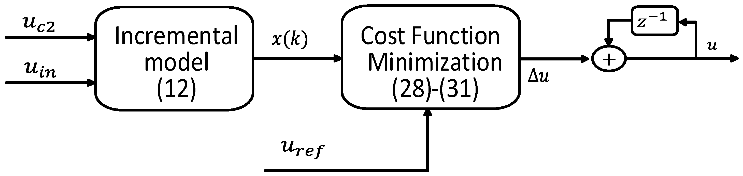
3.3. Model Predictive Control

This approach involves the design of the embedded integrating model for the CCS-MPC controller. For the control signal, a predictive horizon of the current and output voltages of the converter is predicted inside the prediction horizon ( N p ). The control block diagram of the MPC algorithm is shown in Figure 3. The inputs of this block are the input voltage ( u i n ), the output voltage ( u c 2 ), and the reference voltage ( u r e f ). The incremental model (12) generates the estimated vector x ( k ) . The optimal control signal Δ u is achieved using the cost functions (28)–(31). An integrator is embedded in the model to generate the control signal u. Considering the vectors of the future incremental control signals at k j is described below:
Δ U = [ Δ u ( k j ) T Δ u ( k j + N c 1 ) T ] T
where N c is the control horizon, and the prediction of future state variables can be done with the help of given information x ( k j ) for the prediction horizon, N p , with the main objective to find the control signals of the vector dimensions of N c . Assuming an incremental state-space model described by the matrices A , B , and C , and the disturbance vector Δ e ( k ) in (14), the future state variables can be evaluated in sequence from (16):
x ( k j + N p | k j ) = A N p x ( k j ) + A N p 1 B Δ u ( k j ) + A N p 1   E Δ e ( k j ) + A ^ ( N p N c )   B Δ u ( k j + N c 1 ) + A ^ ( N p N c )   E Δ e ( k j + N c 1 )
where x ( k j + N p | k j ) is the future state predicted variables at ( k j + N p ) from the control system x ( k j ) . Similarly, the predicted outputs variable can be achieved from the predicted state variables, as follows:
y ( k j + N p | k j ) = C A N p x ( k j ) + C A N p 1   B Δ u ( k j ) + C A N p 1   E Δ e ( k j ) C A N p N c   B Δ u   ( k j + N c 1 ) + C A N p N c   E Δ e ( k + N c 1 )
It is clearly seen that the predicted future state variables and future control trajectory are stated in terms of x ( k j ) and Δ u , respectively. Thus, the output vector Y can be described as:
Y = [ y ( k j + 1 | k j )   y ( k j + 2 | k j ) y ( k j + N p | k j ) ] T
From (18), a complex matrix form is obtained, expressed as:
Y = F x ( k j ) + G Δ u + H Δ e
where F is a vector of dimension N p , and G , and H are matrices with dimension of N c × N P .
F = ( C A   C A 2   C A 3   C A N p ) T
G = ( C B 0 q × q 0 q × q C A B C B 0 q × q C A N p 1 B C A N p 2 B C A N p N c B )
H = ( C E 0 q × q 0 q × q C A E C E 0 q × q C A N p 1 E C A N p 2 E C A N p N c E )
where q is the number of output variables. In our case q = 1 .
Now, let us define the following cost function:
J = ( Y * Y ) 2 + Δ u T R Δ u
where R = r w I p N c p N c is a diagonal matrix and r w > 0 is the control effort used as a tuning parameter to achieve desired closed-loop performance. Moreover, Y * is the reference variable. Note that the reference is maintained practically constant inside the predictive windows; hence, Y * is expressed as:
Y * ( k j ) = [ I q × q I q × q I q × q N p ] r ( k j )
where r ( k j ) = u i n 2 to achieve the voltage balance between the two DC output voltages.
Then, doing the first derivative of J with respect to Δ u yields:
δ J δ Δ u = 2 G T ( y * F x ( k j ) H Δ d ( k j ) ) + 2 M Δ u
where M = G T G + R . Then, by equalizing (25) to zero and considering the optimal vector in (26), the incremental control signal can be expressed as follows:
Δ u ( k j ) = M 1 G T ( r ¯ y * ( k j ) F x ( k j ) H Δ e ( k j ) )
It is noteworthy that the ∆u shows all incremental values for sampling instant k j to ( k j + N c 1 ). As (13)–(14) are time variants, the incremental control can be stated as a state feedback controller. In line with (15), the actual incremental can be defined as follows:
Δ u ( k j ) = K r   y *   ( k j ) K c x ( k j ) K h   Δ e ( k j ) = K r   ( y *   ( k j ) y ( k j ) ) K x   Δ x m   ( k j ) K h   Δ e ( k )
where:
K r = W ( G G T + R ) 1 r ¯
K c = W ( G G T + R ) 1 F G T
K h = W ( G G T + R ) 1 H G T
Note that K c = [ K x K r ] is the MPC controller gain. Furthermore, according to the principle of receding horizon, W is the   N c dimensional matrix [ I p × q 0 p × q 0 p × q ] . Finally, the optimal control signal can be achieved by adding the incremental value Δ u ( k j ) in the control signal of the previous instant, as follows:
u ( k j ) = Δ u ( k j ) + u ( k j 1 )
or equivalently:
u ( k j ) = u ( k j 1 ) + K r ( y * ( k j ) y ( k j ) ) K x Δ x m K h Δ e ( k j )
The increment of the control signal contains the voltage error, thus performing the integration in discrete form for the control signal that can achieve a zero steady-state error. Bearing this in mind, the duty cycle can be calculated as follows:
d = u ( k j ) = u ( k j 1 ) + K r ( y * ( k j ) y ( k j ) ) K x Δ x m K h Δ e ( k j )
where K r , K x , and K h are the gain obtained by minimizing the cost function (24). Thereby, the converter operations can be properly carried out once the switching periods are calculated, as will be discussed in Section 4.

3.4. Design Guidelines

The control design parameters of the CCS-MPC controller are selected according to the dynamic specifications of the controller. The value of the control effort parameter r w is set based on the compromise between the maximum deviation during the transient response and the settling time, according to the following specifications:
(1)
To achieve the stability of the prediction, horizon N p and control horizon N c are designed large enough [22].
(2)
To accomplish a better transient response under load fluctuations in the bipolar DC bus, the settling time is assigned a value less than 1 ms.
(3)
To achieve a good dynamic response with a low deviation during the transient response, the dominant poles are placed with a damping ratio close to 0.707.
Therefore, the stability analysis of the MPC controller is used to achieve the design specifications. With this in mind, the stability analysis of the proposed system has been developed using the control-loop poles from the small signal model described by (14) and (15). Hence, the closed-loop poles can be calculated as the function of the control effort parameter r w , the prediction and control horizons, N p and N c , and the electrical parameters of the power converter.
Figure 4 shows the position of the closed-loop poles for different prediction and control horizons and sweeping the control effort, r w , from 0 to 10, where blue crosses (x) shows poles with different r w values. In Figure 4a, the values of prediction horizon N p = 5 and control horizon N c = 3 are selected, respectively. For these values of N p and N c , when the value of the control effort r w increases from 0.01   to   10 , the system tends to be unstable, as shown in Figure 4a. In contrast, Figure 4b shows the poles with prediction horizon, N p = 150 and control horizon N c = 50 , the poles move closer to the unitary circle. The system looks stable with the given values of control effort r w . It should be noted that the stability is ensured for the whole range of the control effort r w . Therefore, N p = 150 and N c = 50 are selected for the CCS-MPC controller’s implementation. Finally, based on the given design specifications, the control effort is selected as r w = 0.1 to achieve the required transient performance. In the Figure 4b the red crosses (x) represents the closed loop poles for the designed parameters.

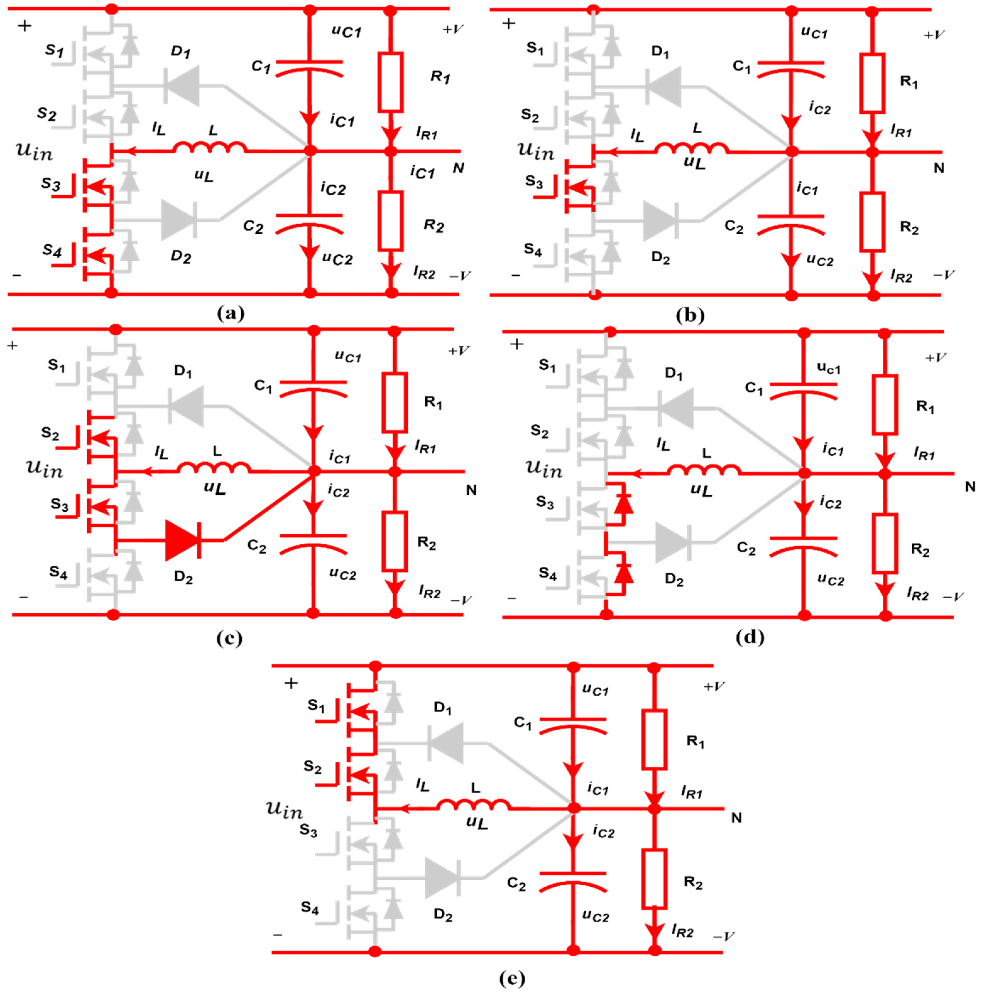
4. Operating Principle of Balancing Converter

Some simplifying assumptions are made. Firstly, the two capacitors C 1 and C 2 are equal, and the output voltage does not change during the switching period. The freewheeling diodes and switches are ideal. The turn on and off periods of the switches are not considered. As depicted in Figure 1b, when the load current of ( I R 2 ) is greater than the load current of ( I R 1 ), the input voltage u i n will transfer a part of the unbalanced power to R 2 through inductor L to balance the output voltages u c 1 and u c 2 . The inductor current is ( I L > 0 ), and during the freewheeling time, when there is no power transfer to the load R 2 , the I L is greater than the difference of I R 2 and I R 1 . In contrast, the inductor current is ( I L < 0 ).

4.1. Operation Principle under State I

The switching time diagrams of the semiconductor power switches S 1 to S 4 , the voltage stress on the power switches, and the inductor current I L are shown in Figure 5, together with the drain-source voltages u s 1 to u s 4 and the across power switches S 1 to S 4 . Altogether, there are eight modes of operation, when ( I L > 0 ) as shown in the equivalent circuits of the balancing converter in Figure 6.
(1)
Mode-I ( t 0 , t 1 )
As shown in Figure 5 and Figure 6a, in this interval, the switch S 1 is turned off and I L runs through D 5 . The value of I L will not change, as the inductor voltage u L is zero, and the voltage of   u s 1 is equal to u c 1 , and the sum of   u s s 3 + u s 4 = u c 2 . Under the balance states u c 1 = u c 2 = 0.5   u i n . Similarly, the voltage stresses across u s 1 , u s 3 , u s 4 are 0.5 u _ i n , 0.25 u i n , and 0.25 u i n , respectively, and the voltage stress on u D 6 is u c 2 u s 4 = 0.25 u i n .
(2)
Mode-II ( t 1 , t 2 )
As shown in Figure 5 and Figure 6b, during the time interval, t 1 to t 2 the switch S 3 is turned on, and I L runs through the D 5 and S 2 . Since switches S 2 and S 3 are turned on, the voltage stress across u S 1 and u s 4 is equal to 0.5. Meanwhile, the voltage stress across u D 6 is equal to zero.
(3)
Mode-III ( t 2 , t 3 )
As shown in Figure 5 and Figure 6c, in this mode, the switch S 2 is turned off and the I L will pass through the freewheeling diodes D 3 and D 4 from S 2 and D 5 .
(4)
Mode-IV ( t 3 , t 4 )
As shown in Figure 5 and Figure 6d, in this mode, the switch S 4 is turned on at the time interval t 3 , and I L passes through D 1 and D 3 , u L decreases to u L = u C 2 , and there is similar voltage stress on the power switches as in the third mode.
(5)
Mode-V ( t 4 , t 5 )
As shown in Figure 5 and Figure 6c, in this mode, the switch S 4 is turned off, and the other conditions are the same as in the fourth mode.
(6)
Mode-VI ( t 5 , t 6 )
As shown in Figure 5 and Figure 6b, in this time interval, the switch S 2 is turned on and I L runs through the D 5 and S 2 from D 3 and D 5 . The value of the I L does not change as the inductor voltage u L = 0 . The voltage stress on all power switches is the same as in the second mode.
(7)
Mode-VII ( t 6 , t 7 )
As shown in Figure 5 and Figure 6a, in this time interval, the switch S 3 is turned off, and I L runs through D 5 and S 2 . In addition, the value of i L does not change as u L = 0 . The voltage stress on S 1 , S 3 and S 4 i s   0.5 u i n and u D 6 is zero.
(8)
Mode-VIII ( t 7 , t 8 )
As shown in Figure 5 and Figure 6e, in this interval, the switch S 1 is turned on, and I L runs through S 1 and S 2 from D 5 .   I L will be increased to u L = u C 1 . The voltage stress on S 3 and S 4 is 0.5 u i n . From t 8 on, the next interval will start.

4.2. Operation Principle under State II

The switching time diagram is depicted in Figure 7. When I L is working under state II, it is seen that the first five modes during the time intervals ( t 0 , t 4 ) and ( t 9 , t 10 ) are the same as in Figure 5. Therefore, only the modes from t 4 to t 9 are discussed here and their equivalent circuit is shown in Figure 8.
(1)
Mode-V ( t 4 ,   t 5 )
As shown in Figure 7 and Figure 8a, in this time interval, the switches S 3 and S 4 are turned on, I L is decreased to zero, and u L = u c 2 . The voltage stress on switches S 1 and S 2 will be u i n 2 , and the voltage stress on u D 5 and u D 6 is zero and u i n 2 , respectively.
(2)
Mode-VI ( t 5 , t 6 )
As shown in Figure 7 and Figure 8b, in this mode, S 4 is turned off and I L passes through S 3 and D 6 . As u L = 0 , I L does not change, and the voltage stress on S 4 is half of the input voltage. The voltage stress on S 1 and S 2 is u i n / 4 . Therefore, the voltage stress on freewheeling diodes u D 5 and u D 6 are u i n / 4 and zero, respectively.
(3)
Mode-VII ( t 6 , t 7 )
As shown in Figure 7 and Figure 8c, in this interval, S 2 is turned on, and I L runs through S 3 and D 6 . The value of I L does not change as u L = 0 . The voltage stress on S 1 and S _ 4 is u i n / 2 and on u D 5 and u D 6 is zero.
(4)
Mode-VIII ( t 7 , t 8 )
As shown in Figure 7 and Figure 8d, in this time interval, S 3 is turned off, I   L runs through D 1 and D 2 , and its value decreases positively. The voltage stress on switches S 3 and S 4 is u i n / 2 , and the voltages stress on u D 5 and u D 6 is u i n / 2 and zero, respectively.
(5)
Mode-IX ( t 8 , t 9 )
As shown in Figure 7 and Figure 8e, in this mode, S1 is turned on and IL runs through D1 and D2. The value of IL decreases to negative uc1. During this mode, the voltage stress on the power switches is similar to mode-VIII. From time t10, the next working period will start, respectively.

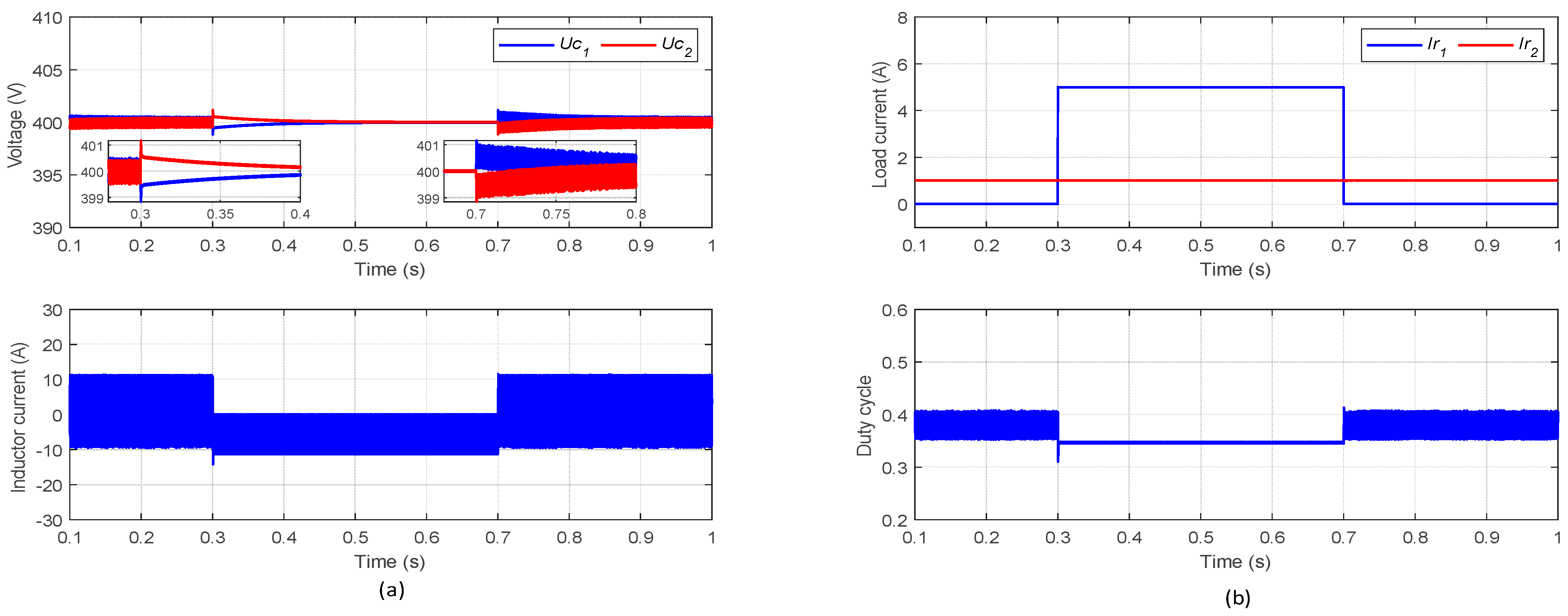
5. Results and Discussion

The dynamic performance evaluation of the proposed improved topological DC bus system, simulated in the MATLAB/Simulink environment with a half-bridge three-level balancing DC–DC converter is considered. In addition, an 800 V charging station with a CCS-MPC control algorithm is developed to validate the proposed architecture. The parameters of the simulated system are listed in Table 1.

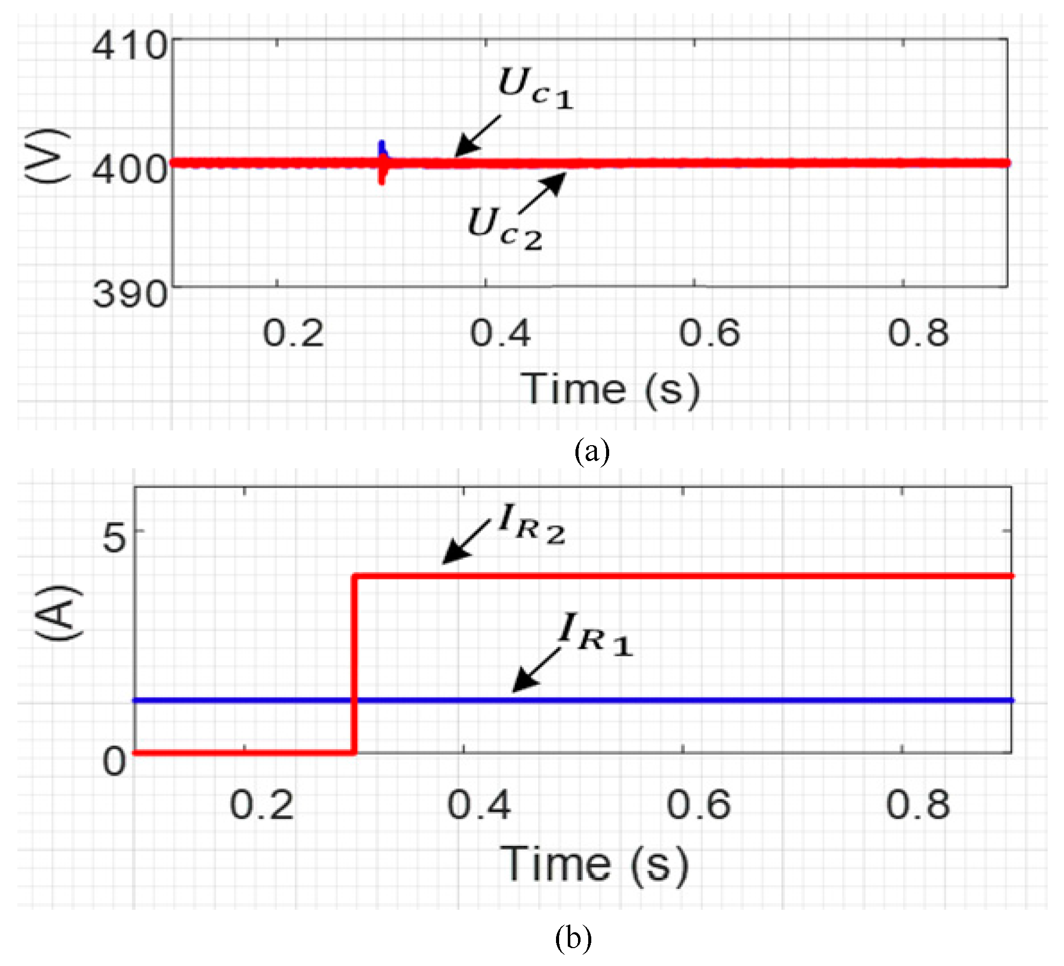
5.1. Steady State Analysis

Figure 9 illustrates the stable waveform under different states, where Figure 9a depicts the switches drain-source voltages, inductor current, and the output voltages. When the load current ( I R 2 > I R 1 ), where I R 1 = 1.2   A , I R 2 = 8.5   A , the output voltages u C 1 and u C 2 are 400.2 V and 399.8 V, respectively. Similarly, Figure 9b shows the drain-source voltages, inductor current, and output voltages when I R 1 = 2.5   A and I R 2 = 5   A , and u C 1 and u C 2 are 400.2 V and 400.1 V, respectively. In this state, I L is always greater than zero.
Figure 9c,d shows the stable numerical waveforms under state II, when IL is either greater or less than zero. Figure 9c shows the switching drain-source voltages, inductor current, and output voltages when the load current IR2 is less than IR1, where IR1 = 7.5 A, IR2 = 1.3 A, and the output voltages uc1 and uc2 are 399.82 V and 400.23 V, respectively. Likewise, Figure 9d shows similar results when IR1 = 5 A, IR2 = 3 A, and uc1 and uc2 are 400 V and 400.2 V, respectively.
According to Figure 9, the simulation results show that the voltage stress on switches is half of the input voltage, which validates the theoretical analysis shown in Figure 5 and Figure 7. The reason behind the voltage spikes of the drain-source voltages is due to the resonance when the switches are turned off. It is seen that the output voltages u c 1 and u c 2 are very close to 400 V when using the MPC controller in both states.

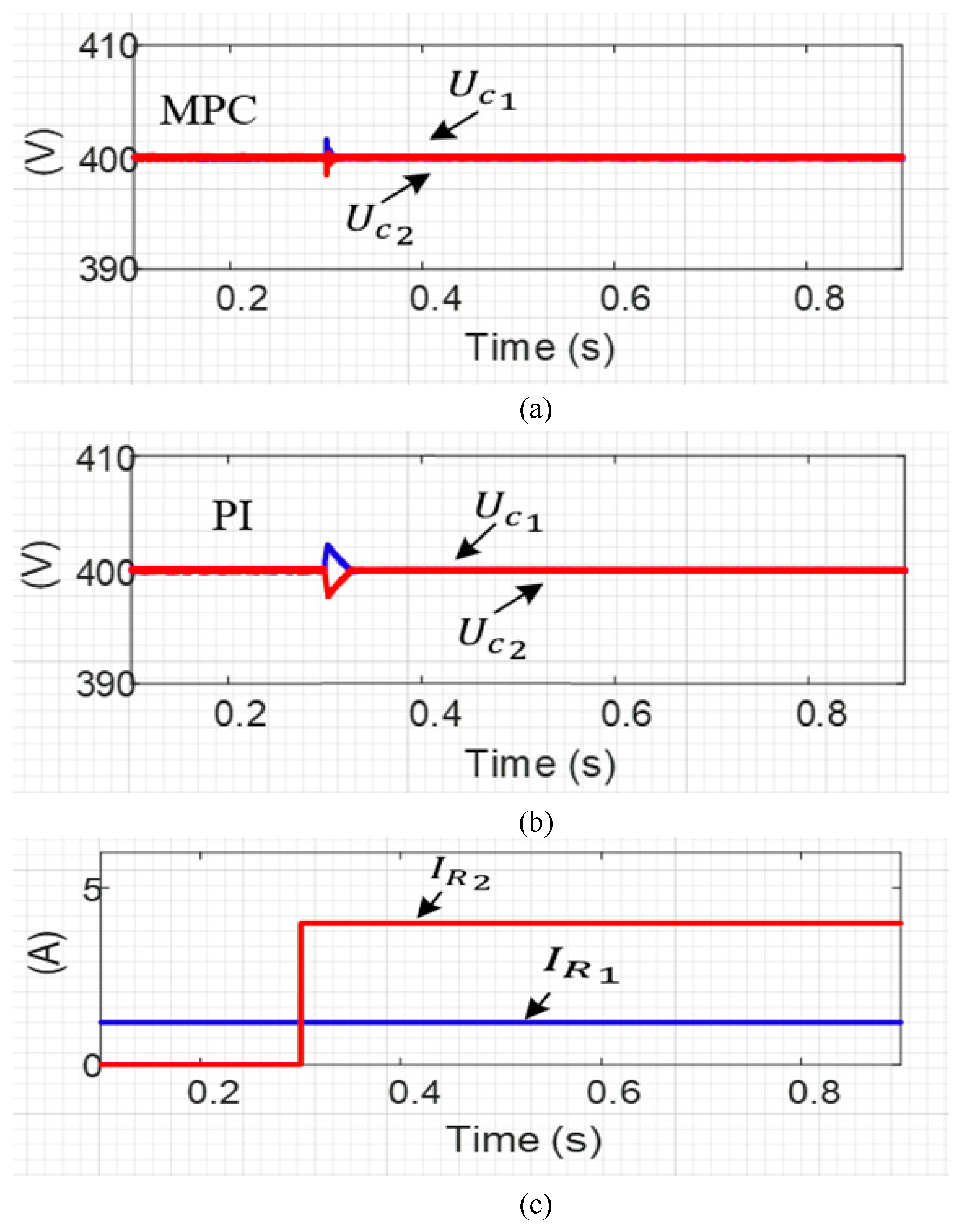
5.2. Performance Comparison of Transient Load Response

This subsection presents a comparison between the proposed control and previous state-of-the-art controllers. For this purpose, the proposed CCS-MPC will be compared with the PI controller presented in [16]. In order to conduct a fair comparison, the PI controller was designed using a genetic algorithm to optimize the control gains, hence improving the transient response due external disturbances such as sudden load changes.
The optimal GA-PI control gains are shown in Table 1 as K p and K i for the proportional gain and integral gain, respectively.
In order to validate the dynamic performance of the proposed control scheme, one simulation test was performed. For this purpose, the controllers were tested under a sudden load change. This simulation test has the following pattern. From t = 0 s to t = 0.3 s, I R 1 = 0   A and I R 2 = 1   A . Then, at t = 0.3 s, I R 1 increases to a value equal to 5 A, while I R 2 remains constant. Finally, at t = 0.7 s, I R 1 decreases to 0 A and I R 2 remains constant. Figure 10 and Figure 11 show the numerical results under transient load changes, using the proposed CCS-MPC and the GA-PI, respectively. In both cases, the u C 1 and u C 2 are almost equal, although they have apparent fluctuations during load transients. Moreover, the proposed CCS-MPC-based control strategy tracks the reference voltages with negligible fluctuations, while there are apparently large fluctuations in the case of the GA-PI controller due to its faster and smoother transient response with lesser control complexity than the conventional linear controller. In addition, the MPC has a lower rising time, settling time, and overshoots than the GA-PI controller. Moreover, the CCS-MPC controller reduces the dangerous oscillations in the inductor and provides a smoother operation under load transients. At the same time, the conventional PI controller has more fluctuations in the output voltages with considerable ripples before and after the load transients. The proposed CCS-MPC considerably reduces the current over the inductor, thus allowing a reduction in the filter components.

5.3. Parameter Robustness Analysis

To confirm the parameter robustness of the proposed CCS-MPC controller against parameter uncertainty, the simulation results were compared with the designed GA-PI controller by changing the inductance and capacitance of the balancing converter.
Firstly, the proposed CCS-MPC and conventional GA-PI controller with a nominal inductance of 5 mH were tested at the 50% inductance nominal value. Figure 12 shows the output voltages and inductor current of the proposed CCS-MPC scheme with an inductance of 2.5 mH, and Figure 13 depicts the output voltages and inductor current of the GA-PI controller with a 2.5 mH inductance value. It is apparent that the conventional PI controller has an oscillatory behavior, while the CCS-MPC is more robust in case of an inductor parameter mismatch.
Secondly, to verify the robustness of the proposed CCS-MPC against the capacitance mismatch, the capacitance of the balancing converter was set to 235 μ F , which is 50% of the nominal value. Figure 14 shows the dynamic output voltages and the inductor current of the CCS-MPC control schemes, while Figure 15 shows the dynamics of the GA-PI controller. The proposed CCS-MPC shows robust control of the output voltages as well as in the inductor current. In contrast, the conventional GA-PI controller has apparent output voltage deviations and inductor current ripples under the capacitance mismatch.

5.4. Experimental Results

To validate the system performance, the experimental results of the proposed control scheme were carried out using the dSPACE 1006 platform for real-time control, as depicted in Figure 16.
Figure 17 and Figure 18 show the hardware-in-loop (HIL) results under the transient load changes. Figure 17 shows the transient load response of the MPC when the load I R 1 is increasing, while Figure 18 shows the response of the proposed scheme when I R 2 is increasing.
Figure 19 and Figure 20 show the HIL results under the transient load with the CCS-MPC and PI controller. Figure 19a shows the output voltage response with the MPC, while Figure 19b shows the output voltage response with the GA-PI controller under transient load conditions, as shown in Figure 19c. Similarly, Figure 20a,b show the performance response of the MPC and GA-PI controller, respectively, when load I R 2 is increasing, as shown in Figure 20c. In both cases, the proposed CCS-MPC-based control strategy tracks the reference voltages with negligible fluctuations, while there are apparently large fluctuations in the case of the PI controller.

5.5. Comparative Analysis

In Table 2, the performance comparison with regard to the proposed MPC is compared with the PI controller. Note that there is better accuracy in tracking with the MPC controller.
The DC link voltages, i.e., U C 1   and U C 2 , are observable in the case of the MPC controller. Moreover, the proposed MPC approach also provides less peak-to-peak deviation in the voltage ripples when different test cases are performed with respect to load current variations I R 1 and I R 2 . As a result, less heating in the loads is evident, since the peak-to-peak load ripple is lesser in magnitude. Nevertheless, the computational complexity of the proposed MPC is slightly higher than for GA-PI. However, the proper tuning of a PI controller is a tedious task to achieve for gaining high robustness. Hence, the proposed MPC is a suitable choice for meeting the objectives of better control with a three-level DC–DC converter compared to PI controllers.

6. Conclusions

In this paper, an enhanced CCS-MPC-based bipolar EV charging station is proposed under a MATLAB/Simulink environment, and the HIL experimental results are verified. A three-level balancing converter with an improved CCS-MPC control strategy is applied to make this system bipolar and balance the DC bus. The operation principle of the balancing converter is analyzed, and its stability analysis is developed for selecting the control parameters of the proposed control strategy. Our results indicate that this topology helps to solve the shoot-through problem by building a neutral line to balance the DC buses for different loads in EV charging stations. The proposed control strategy, with a three-level balancing converter, has lower voltage and current stresses on semi-conductor devices and can balance the DC bus voltages with extremely unbalanced load conditions. The numerical results corroborate the fact that the proposed CCS-MPC controller can better balance the bipolar DC CS under load fluctuations than the optimal GA-PI controller. In the bipolar DC CS, the proposal can complete the control with a reduced computational burden, which greatly saves the cost. However, more research is still needed in order to further optimize and validate the proposed design and thus, this paper opens a new research topic potentially leading to the implementation of the MPC in bipolar DC microgrids.
As the use of EVs is becoming more popular, the modern infrastructure of EVs is also developing toward the zero-emission goal. Therefore, the MPC approaches can be used in the design and development of bipolar-based DC EV charging stations. As an open topic for future research, the application of reinforcement learning algorithms and neuro-adaptive approaches in the design of the MPC can be studied.

Author Contributions

M.S.: investigation, conceptualization, methodology, software, writing—original draft; C.A.A.: conceptualization, methodology, validation; Y.T.: writing—review and editing; S.W.A.: data curation, conceptualization; C.-L.S.: supervision, writing—review and editing; Ľ.B.: visualization, validation, conceptualization, writing—review and editing; C.-H.L.: writing—review and editing; M.E.: methodology, writing—review and editing. All authors have read and agreed to the published version of the manuscript.

Funding

The work of Lubos Buzna was supported in part by the Scientific Grant Agency of the Ministry of Education, Science, Research and Sport of the Slovak Republic under the project VEGA 1/0077/22 “Innovative prediction methods for optimization of public service systems” and project VEGA 1/0216/21 “Design of emergency systems with conflicting criteria with the tools of artificial intelligence”, in part by the Slovak Research and Development Agency under the project APVV-19-0441 “Allocation of limited resources to public service systems with conflicting quality criteria”, and in part by the Operational Program Integrated Infrastructure 2014–2020 “Innovative Solutions for Propulsion, Power, and Safety Components of Transport Vehicles” through the European Regional Development Fund under grant ITMS313011V334. The works of Chun-Lien Su and Mahmoud Elsisi were funded by the Ministry of Science and Technology of Taiwan under grant MOST 110-2221-E-992-044-MY3 and MOST 110-2222-E-011-013.

Institutional Review Board Statement

Not applicable.

Informed Consent Statement

Not applicable.

Data Availability Statement

Not applicable.

Conflicts of Interest

The authors declare no conflict of interest.

References

  1. Tan, L.; Zhu, N.; Wu, B. An Integrated Inductor for Eliminating Circulating Current of Parallel Three-Level DC-DC Converter-Based EV Fast Charger. IEEE Trans. Ind. Electron. 2016, 63, 1362–1371. [Google Scholar] [CrossRef]
  2. Tan, L.; Wu, B.; Rivera, S.; Yaramasu, V. Comprehensive DC Power Balance Management in High-Power Three-Level DC-DC Converter for Electric Vehicle Fast Charging. IEEE Trans. Power Electron. 2016, 31, 89–100. [Google Scholar] [CrossRef]
  3. Khan, W.; Ahmad, A.; Ahmad, F.; Alam, M.S. A Comprehensive Review of Fast Charging Infrastructure for Electric Vehicles. Smart Sci. 2018, 6, 256–270. [Google Scholar] [CrossRef]
  4. Rafi, M.A.H.; Bauman, J. A Comprehensive Review of DC Fast-Charging Stations with Energy Storage: Architectures, Power Converters, and Analysis. IEEE Trans. Transp. Electrif. 2021, 7, 345–368. [Google Scholar] [CrossRef]
  5. Mutarraf, M.U.; Terriche, Y.; Nasir, M.; Guan, Y.; Su, C.L.; Vasquez, J.C.; Guerrero, J.M. A Communication-Less Multimode Control Approach for Adaptive Power Sharing in Ship-Based Seaport Microgrid. IEEE Trans. Transp. Electrif. 2021, 7, 3070–3082. [Google Scholar] [CrossRef]
  6. Mutarraf, M.U.; Terriche, Y.; Niazi, K.A.K.; Vasquez, J.C.; Guerrero, J.M. Energy storage systems for shipboard microgrids—A review. Energies 2018, 11, 3492. [Google Scholar] [CrossRef]
  7. Gwon, G.H.; Kim, C.H.; Oh, Y.S.; Noh, C.H.; Jung, T.H.; Han, J. Mitigation of voltage unbalance by using static load transfer switch in bipolar low voltage DC distribution system. Int. J. Electr. Power Energy Syst. 2017, 90, 158–167. [Google Scholar] [CrossRef]
  8. Liao, J.; You, X.; Liu, H.; Huang, Y. Voltage stability improvement of a bipolar DC system connected with constant power loads. Electr. Power Syst. Res. 2021, 201, 107508. [Google Scholar] [CrossRef]
  9. Rivera, S.; Wu, B. Electric Vehicle Charging Station With an Energy Storage Stage for Split-DC Bus Voltage Balancing. IEEE Trans. Power Electron. 2017, 32, 2376–2386. [Google Scholar] [CrossRef]
  10. Verma, A.K.; Subramanian, C.; Jarial, R.K.; Roncero-Sanchez, P. An Enhanced Discrete-Time Oscillator-Based PLL-Less Estimation of Single-Phase Grid Voltage Parameters. IEEE Trans. Ind. Electron. 2022, 69, 3977–3987. [Google Scholar] [CrossRef]
  11. Tan, L.; Wu, B.; Yaramasu, V.; Rivera, S.; Guo, X. Effective Voltage Balance Control for Bipolar-DC-Bus-Fed EV Charging Station with Three-Level DC-DC Fast Charger. IEEE Trans. Ind. Electron. 2016, 63, 4031–4041. [Google Scholar] [CrossRef]
  12. Tian, Q.; Zhou, G.; Leng, M.; Xu, G.; Fan, X. A Nonisolated Symmetric Bipolar Output Four-Port Converter Interfacing PV-Battery System. IEEE Trans. Power Electron. 2020, 35, 11731–11744. [Google Scholar] [CrossRef]
  13. Zhang, X.; Gong, C.; Yao, Z. Three-level DC converter for balancing DC 800-V voltage. IEEE Trans. Power Electron. 2015, 30, 3499–3507. [Google Scholar] [CrossRef]
  14. Zhang, X.; Gong, C. Dual-buck half-bridge voltage balancer. IEEE Trans. Ind. Electron. 2013, 60, 3157–3164. [Google Scholar] [CrossRef]
  15. Han, B.M. A half-bridge voltage balancer with new controller for bipolar DC distribution systems. Energies 2016, 9, 182. [Google Scholar] [CrossRef]
  16. Zhang, X.; Zhu, H.; Song, Y.; Li, R. Three-level dual-buck voltage balancer with active output voltagesbalancing. IET Power Electron. 2019, 12, 2987–2995. [Google Scholar] [CrossRef]
  17. Dc, B. A Bi-Directional Dual-Input Dual-Output Converter for Voltage Balancer in Bipolar DC Microgrid. Energies 2022, 15, 5043. [Google Scholar]
  18. Liu, J.; Vazquez, S.; Wu, L.; Marquez, A.; Gao, H.; Franquelo, L.G. Extended State Observer-Based Sliding-Mode Control for Three-Phase Power Converters. IEEE Trans. Ind. Electron. 2017, 64, 22–31. [Google Scholar] [CrossRef]
  19. Wang, X.; Wu, M.; Ouyang, L.; Tang, Q. The application of GA-PID control algorithm to DC-DC converter. In Proceedings of the 29th Chinese Control Conference, Beijing, China, 29–31 July 2010; pp. 3492–3496. [Google Scholar]
  20. Al-Tameemi, Z.H.A.; Lie, T.T.; Foo, G.; Blaabjerg, F. Optimal Coordinated Control of DC Microgrid Based on Hybrid PSO–GWO Algorithm. Electricity 2022, 3, 346–364. [Google Scholar] [CrossRef]
  21. Yang, G.; Yao, J.; Ullah, N. Neuroadaptive control of saturated nonlinear systems with disturbance compensation. ISA Trans. 2022, 122, 49–62. [Google Scholar] [CrossRef]
  22. Rossiter, J.A. Model-Based Predictive Control: A Practical Approach; CRC Press: Boca Raton, FL, USA, 2017; pp. 1–318. [Google Scholar]
  23. Guzman, R.; de Vicuna, L.G.; Camacho, A.; Miret, J.; Rey, J.M. Receding-Horizon Model-Predictive Control for a Three-Phase VSI with an LCL Filter. IEEE Trans. Ind. Electron. 2019, 66, 6671–6680. [Google Scholar] [CrossRef] [Green Version]
  24. Alfaro, C.; Guzman, R.; de Vicuna, L.G.; Miret, J.; Castilla, M. Dual-Loop Continuous Control Set Model-Predictive Control for a Three-Phase Unity Power Factor Rectifier. IEEE Trans. Power Electron. 2022, 37, 1447–1460. [Google Scholar]
  25. Zhou, D.; Jiang, C.; Quan, Z.; Li, Y. Vector Shifted Model Predictive Power Control of Three-Level Neutral-Point-Clamped Rectifiers. IEEE Trans. Ind. Electron. 2020, 67, 7157–7166. [Google Scholar] [CrossRef]
  26. Vargas, R.; Member, S.; Cortés, P.; Ammann, U.; Rodríguez, J.; Member, S.; Pontt, J. Predictive Control of a Three-Phase. IEEE Trans. Ind. Electron. 2007, 54, 2697–2705. [Google Scholar] [CrossRef]
  27. Liu, X.; Qiu, L.; Fang, Y.; Ma, J.; Wu, W.; Peng, Z.; Wang, D. Lyapunov-based finite control-set model predictive control for nested neutral point-clamped converters without weighting factors. Int. J. Electr. Power Energy Syst. 2020, 121, 106071. [Google Scholar] [CrossRef]
  28. Geyer, T.; Mastellone, S. Model predictive direct torque control of a five-level ANPC converter drive system. IEEE Trans. Ind. Appl. 2012, 48, 1565–1575. [Google Scholar] [CrossRef]
  29. Cortes, P.; Wilson, A.; Kouro, S.; Rodriguez, J.; Abu-Rub, H. Model predictive control of multilevel cascaded H-bridge inverters. IEEE Trans. Ind. Electron. 2010, 57, 2691–2699. [Google Scholar] [CrossRef]
  30. Dekka, A.; Wu, B.; Yaramasu, V.; Fuentes, R.L.; Zargari, N.R. Model Predictive Control of High-Power Modular Multilevel Converters—An Overview. IEEE J. Emerg. Sel. Top. Power Electron. 2019, 7, 168–183. [Google Scholar] [CrossRef]
  31. Yang, Y.; Wen, H.; Fan, M.; He, L.; Xie, M.; Chen, R.; Norambuena, M.; Rodriguez, J. Multiple-Voltage-Vector Model Predictive Control with Reduced Complexity for Multilevel Inverters. IEEE Trans. Transp. Electrif. 2020, 6, 105–117. [Google Scholar] [CrossRef]
  32. Lezana, P.; Aguilera, R.; Quevedo, D.E. Model predictive control of an asymmetric flying capacitor converter. IEEE Trans. Ind. Electron. 2009, 56, 1839–1846. [Google Scholar] [CrossRef]
  33. Alfaroaragon, C.A.; Guzman, R.; de Vicuna, L.G.; Miret, J.; Castilla, M. Constrained Predictive Control Based on a Large-Signal Model for a Three-Phase Inverter Connected to a Microgrid. IEEE Trans. Ind. Electron. 2021, 69, 6497–6507. [Google Scholar] [CrossRef]
  34. Preindl, M.; Bolognani, S. Comparison of direct and PWM model predictive control for power electronic and drive systems. In Proceedings of the 2013 Twenty-Eighth Annual IEEE Applied Power Electronics Conference and Exposition (APEC), Long Beach, CA, USA, 17–21 March 2013; pp. 2526–2533. [Google Scholar]
  35. Cavanini, L.; Cimini, G.; Ippoliti, G.; Bemporad, A. Model predictive control for pre-compensated voltage mode controlled DC-DC converters. IET Control Theory Appl. 2017, 11, 2514–2520. [Google Scholar] [CrossRef] [Green Version]
  36. Rajesh, J.; Nisha, K.S.; Bonala, A.K.; Sandepudi, S.R. Predictive Control of Three level Boost Converter Interfaced SPV System for Bi-polar DC Micro grid. In Proceedings of the 2019 IEEE International Conference on Electrical, Computer and Communication Technologies (ICECCT), Coimbatore, India, 20–22 February 2019; pp. 9–14. [Google Scholar]
  37. Nisha, K.S.; Gaonkar, D.N. Model predictive control of three level buck/boost converter for bipolar DC microgrid applications. In Proceedings of the 2019 IEEE 16th India Council International Conference (INDICON), Rajkot, India, 13–15 December 2019; pp. 2019–2022. [Google Scholar]
  38. Du, Y.; Zhou, X.; Bai, S.; Lukic, S.; Huang, A. Review of non-isolated bi-directional DC-DC converters for plug-in hybrid electric vehicle charge station application at municipal parking decks. In Proceedings of the 2010 Twenty-Fifth Annual IEEE Applied Power Electronics Conference and Exposition (APEC), Palm Springs, CA, USA, 21–25 February 2010; pp. 1145–1151. [Google Scholar]
Figure 1. Structure of bipolar DC charging station (a) with independent converters and loads, and (b) diagram of the three-level balancing DC–DC converter.
Mathematics 10 03444 g001
Figure 2. Schematic illustrating the topology of the controller for three-level DC–DC converter.
Mathematics 10 03444 g002
Figure 3. Control block diagram of CCS-MPC.
Mathematics 10 03444 g003
Figure 4. CCS–MPC closed − loop poles for r w variation from 0–10. (a) N p = 5, N c = 3. (b) N p = 150, and N c = 50.
Mathematics 10 03444 g004
Figure 5. Main driving waveforms under state I.
Mathematics 10 03444 g005
Figure 6. Three-level balancing converter equivalent circuit under state I. (a) Mode-I and VII. (b) Mode-II and VI. (c) Mode-III and V. (d) Mode-IV. (e) Mode-VIII. The corresponding voltages are displayed in Figure 5.
Mathematics 10 03444 g006
Figure 7. Main driving waveforms under state II.
Mathematics 10 03444 g007
Figure 8. Three-level balancing converter equivalent circuit under state II. (a) Mode-V. (b) Mode-VI. (c) Mode-VII. (d) Mode-VIII. (e) Mode-IX. The corresponding voltages are displayed in Figure 7.
Mathematics 10 03444 g008
Figure 9. Switching drain-source voltages, inductor current (IR1), and output voltages. (a) State I. (b) State II. (c) State III. (d) State IV.
Mathematics 10 03444 g009
Figure 10. I R 1 Load transient response using the proposed CCS–MPC. (a) Inductor current and output voltages. (b) Duty cycle and load current.
Mathematics 10 03444 g010
Figure 11. I R 1 Load transient response using the GA–PI controller. (a) Inductor current and output voltages. (b) Duty cycle and load current.
Mathematics 10 03444 g011
Figure 12. Numerical results with 50% inductance nominal value using the proposed CCS–MPC. (a) Inductor current and output voltages. (b) Duty cycle and load current.
Mathematics 10 03444 g012
Figure 13. Numerical results with 50% inductance nominal value using the GA–PI controller. (a) Inductor current and output voltages. (b) Duty cycle and load current.
Mathematics 10 03444 g013
Figure 14. Numerical results with 50% capacitance nominal value using the proposed CCS–MPC. (a) Inductor current and output voltages. (b) Duty cycle and load current.
Mathematics 10 03444 g014
Figure 15. Numerical results with 50% capacitance nominal value using the GA–PI controller. (a) Inductor current and output voltages. (b) Duty cycle and load current.
Mathematics 10 03444 g015
Figure 16. Hardware-in-loop experimental setup.
Mathematics 10 03444 g016
Figure 17. Experimental results under transient load conditions when I R 1 is increasing. (a) Output voltages. (b) Load currents.
Mathematics 10 03444 g017
Figure 18. Experimental results under transient load conditions when I R 2 is increasing. (a) Output voltages. (b) Load currents.
Mathematics 10 03444 g018
Figure 19. Experimental results. (a) Transient load response with MPC. (b) Transient load response with PI. (c) When load I R 1 is increasing.
Mathematics 10 03444 g019
Figure 20. Experimental results. (a) Transient load response with MPC. (b) Transient load response with PI. (c) When load I R 2 is increasing.
Mathematics 10 03444 g020
Table 1. System parameters.
DescriptionSymbolValue
Capacitors C 1 = C 2 470   ( μ F )
Inductor L 500   ( μ H )
Switches S 1 S 4 SPW47N60C3
Diodes D 5 , D 6 DESI60-06A
Freewheeling time T f 7.5   μ s
DC bias voltage U B i a s 0.025   V
Input voltage u i n 800   V
Output voltage u C 1 ,   u C 2 About 400   V
Amplitude of carrying wave U p p 12   V
Switching frequency f 25   kHz
Dead time T d 2   μ s
Control horizon N c 50
Prediction horizon N p 150
Control effort r ω 0.1
Proportional gain K p 0.0557
Integral gain K i 0.7508
Table 2. Comparative analysis.
MPC U C 1 (V) U C 2 ( V ) I R 1 (A) I R 2 (A) Δ V
400.2399.81.28.50.2
400.2400.12.550.1
399.82400.237.51.3−0.41
400400.253−0.2
PI396.17401.31.28.5−5.13
397.41400.82.55−3.39
398.1402.77.51.3−4.6
396.5400.1353−3.63
Computational Complexity
Memory statesAddition operatorsDivision operatorsSubtraction operatorsMultiplication operators
MPC31053
PI12013
Performance Indices
Settling timeLoad disturbance rejectionOvershoots in DC link voltageSteady-state errorMismatches in Parameter robustness
MPC1 msGood1.5 V0.5 VGood
PI100 msGood 2 V5 VPoor
Publisher’s Note: MDPI stays neutral with regard to jurisdictional claims in published maps and institutional affiliations.

