Abstract
The use of micro-contacts has been demonstrated in various radio frequency (RF) applications. However, the premature failure of such devices under alternating current (AC) operations is still a hurdle to further development. In this work, modified gray scale lithography is performed to fabricate two types of gold–gold (Au–Au) micro-contacts: hemispherical-planar and hemispherical-2D pyramid. The performance of these devices was investigated under low frequency, low amplitude AC conditions with external circuit loads. A custom-made experimental setup which uses various load configurations, controls the frequency of the applied voltage and modifies the cycle rate of switch operation to obtain the contact resistance as a function of number of cycles (up to 107 cycles). Nearly 87% of the tested devices (13 out of 15 hemispherical-planar micro-contacts) were found to be in good operational condition and passed the 10 million cycle mark successfully. A steady gain and large swing in the value of contact resistance was also observed near the end of all, but one, tests. Such changes in contact resistance were found to be permanent as none of the devices recovered completely. On the other hand, the hemispherical-2D pyramid micro-contact performed better than the planar one as it also passed 107 cycle mark with low and remarkably stable contact resistance throughout the testing span. This study suggests that micro-contacts with ‘engineered’ surface structures with external loads applied are a viable solution to premature failure and high contact resistance in micro-contacts under low frequency AC operations.
1. Introduction
Micro-contacts have been the center of active research for years due to their potential use in various RF applications, such as telecommunications and remote sensing [1,2,3]. Despite such intense research, there are specific concerns that need to be resolved to improve their performance and lifetime. One of the major concerns is the need for an explanation of the failure mechanism of micro-switches in alternating current (AC) conditions. Most of the current explanations are based on and developed from direct current (DC) measurements and cannot readily explain micro-contact behavior under high frequency AC conditions where frequency adds to the complexity.
One possible solution then is to first gain an understanding of the micro-switch response at lower frequencies to provide essential insight into the fundamentals that help to explain higher frequency behavior. However, in a previous study on the effect of low frequency AC conditions, device failure occurred between 103–105 cycles which was much lower than the set target of 107 switching cycles [4]. Such short lifetimes may be attributed to electromigration effect, where contacts failed, closed or shorted due to excessive material transfer [5]. In a previous work, we showed significant improvement in device reliability by using specific external loads (e.g., series and parallel configurations) under DC switching conditions [6]. In [7], Liu et al. investigated an external parallel protective circuit with a series microswitch resulting in an enhanced switching lifetime of more than 100 M cycles. They found that while the parallel configuration increased the total OFF state capacitance, it also degraded the signal isolation capability. Later, in [8], a series protective circuit with a series microswitch was investigated, demonstrating switching lifetimes of more than 500 M cycles with improved isolation. All of these investigations were carried out to enhance the hot switching reliability at radio frequency (RF). A similar approach may also improve the performance and lifetime of micro-switches under low frequency AC conditions [4]. Therefore, the primary focus of this work is to use external loads to improve the reliability of micro-contacts and to investigate their responses under such conditions.
In addition, it has also been reported that the effective conduction area between the top and bottom contact depends on surface contamination which can affect the contact resistance (RC) of micro-contacts [9]. This suggests that micro-contacts with different surface features might behave differently and can also offer a solution to premature device failure. In fact, we have reported that the RC of hemispherical-2D pyramid micro-contacts is much more stable than that of hemispherical-planar micro-contacts (where RC increases with # of cycles) [10]. However, the effect of external loading on the performance of hemispherical-2D pyramid micro-contacts under AC conditions has not been reported. Therefore, a brief discussion on this concern is also addressed in this paper.
2. Test Setup and Device Fabrication
2.1. Test Stand
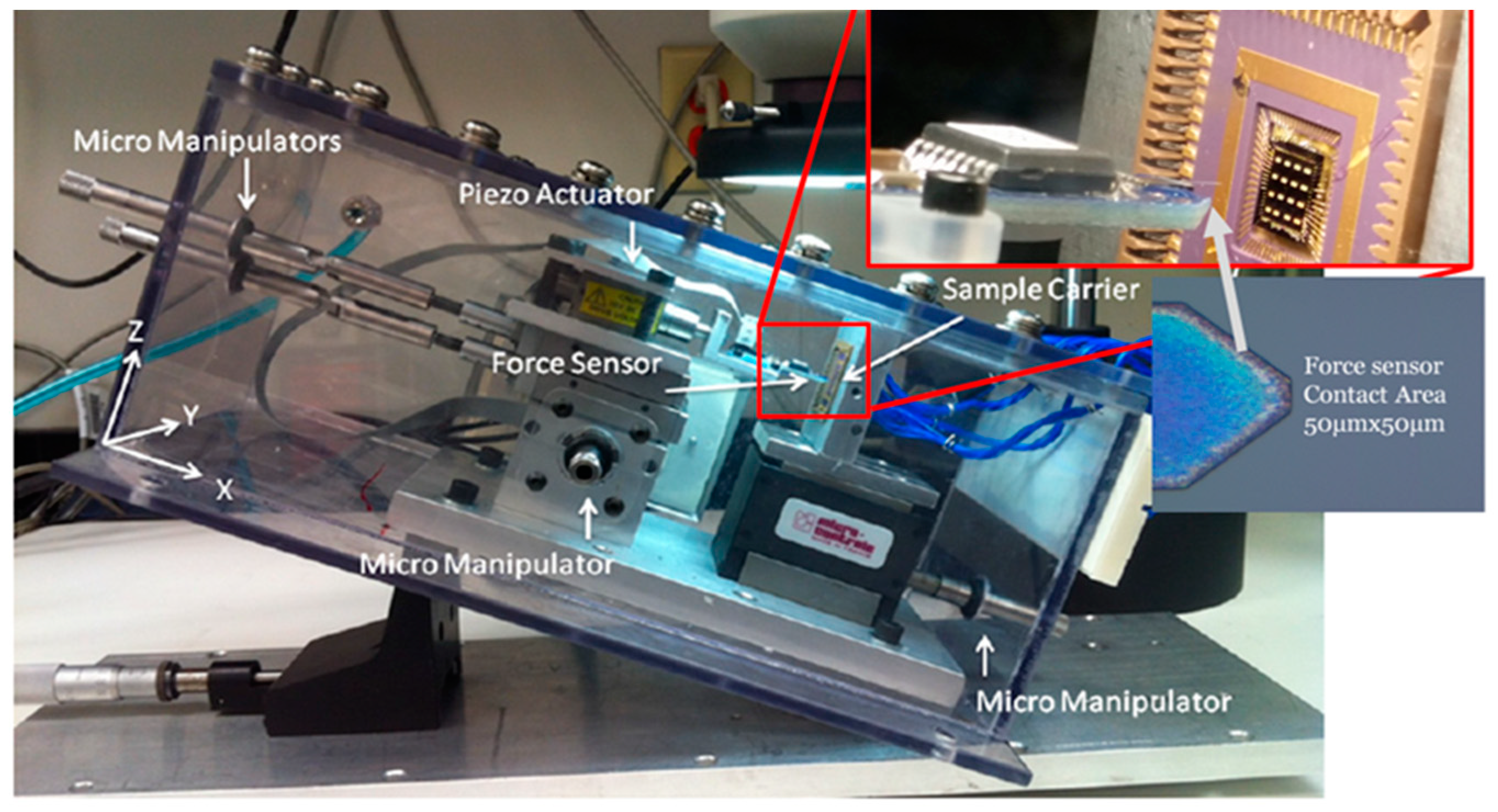
A specifically-designed test stand, shown in Figure 1, was used to characterize the performance and reliability of micro-contacts over the lifetime of 107 cycles. The main part of this instrument is a piezo-controlled force sensor assembly which allows the actuation of a micro-contact to a desired contact force in a dry nitrogen (N2) enclosure. Here, the N2 enclosure is necessary as it reduces the impact of atmospheric contaminations during testing. Furthermore, there are three micro-manipulators which control the movement in the x-, y- and z-axes and align the force sensor with micro-contact support structure (shown in Figure 2a). Under the operation of a controlled contact force, RC is obtained from current and voltage measured using an NI-4070 Flex DMM module (±110 nΩ accuracy) which can either be presented as a function of a contact force or from applied cycles.

Figure 1.
Test stand with externally actuated force sensor assembly. A test reticle of 16 devices is shown in the inset.
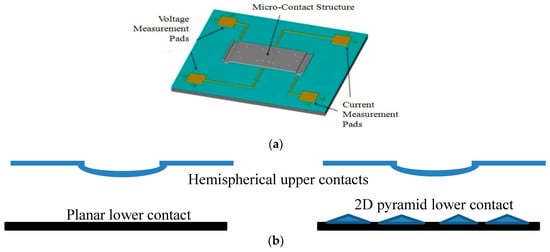
Figure 2.
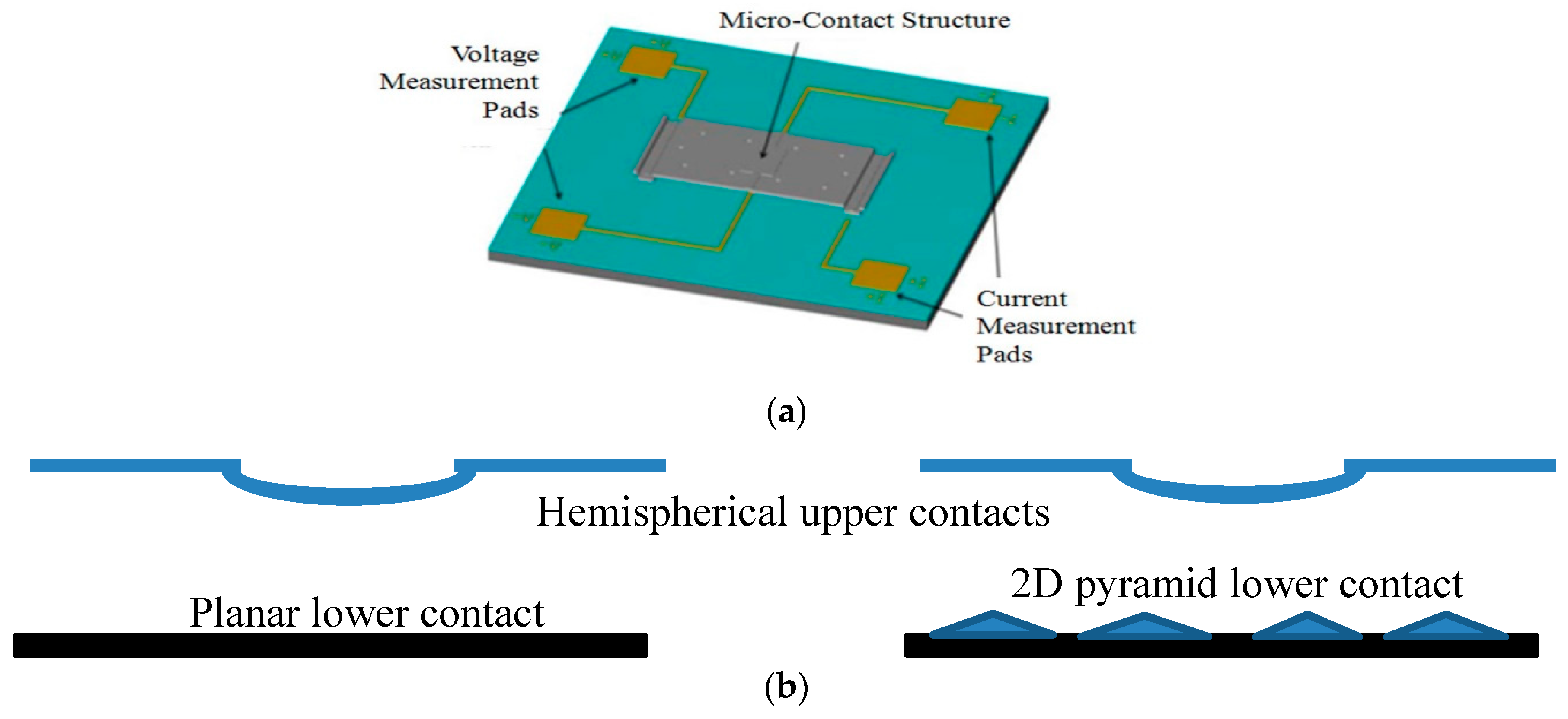
(a) Schematic of a micro-contact fabricated with a hemispherical contact bump on the lower side of the upper support beam; (b) Physical representation of different lower pads used in this study.
This test stand was used not only to measure the RC but also to cycle the devices up to 2.5 kHz, which simulated the cycling encountered during lifetime wear. During this cycling test, an electrical load was applied, which more accurately represented actual usage during a typical device’s lifetime. The electrical load was supplied from a function generator that was synchronized to the mechanical movement of the micro-contact. In this study, all loading was strictly “colds witched”: no voltage potential was present during contact closure and current was reduced to 0 Amps prior to contact opening. Because of the time required for a full cycle at low frequencies, the testing time was reduced sufficiently so that only a single cycle of AC was applied during each switching cycle.
2.2. Micro-Contact Design
The micro-contact support structures used in this study were emulated by a Holm’s crossed bar configuration on the micro-scale, i.e., a fixed-fixed beam structure [9]. This design allows a four-wire measurement where current only flows through the micro-contact during each measurement. Voltage is measured across the micro-contact via gold traces connected to the anchor of the beam and micro-contact area. Figure 2a shows a 3D model of a micro-contact with four contact points required for the testing.
The fixed-fixed beam structures used in this study, were designed with a gap of 1–2 µm between the upper contact bump and lower contact pad. Such structures allow the piezo actuator to close the contact by applying a precise contact force on the top bump. In this study, the structure of the top contact remained constant; a hemispherical bump of ~8 µm (or ~4 µm for the engineered surface lower contacts) radius protruded (~50–100 nm) from the lower surface of an electroplated gold beam. However, two surface structures (i.e., planar and 2D pyramid) were used for the bottom contact pads. The cross-sectional view of such micro-contacts is shown in Figure 2b. Here, 2D pyramids were fabricated by using gray-scale lithography (GSL). A brief discussion of this novel GSL technique is given in the following section.
2.3. Gray-Scale Lithography
In standard lithography, an ultra-violet (UV) exposed area of photoresist (PR) either dissolves completely or remains intact (either positive or negative PR) during pattern development. This binary behavior is useful in the fabrication of planar structures but not very efficient when making 3D structures. Therefore, gray-scale lithography was developed to create multilayer patterns in photoresist using a single development step.
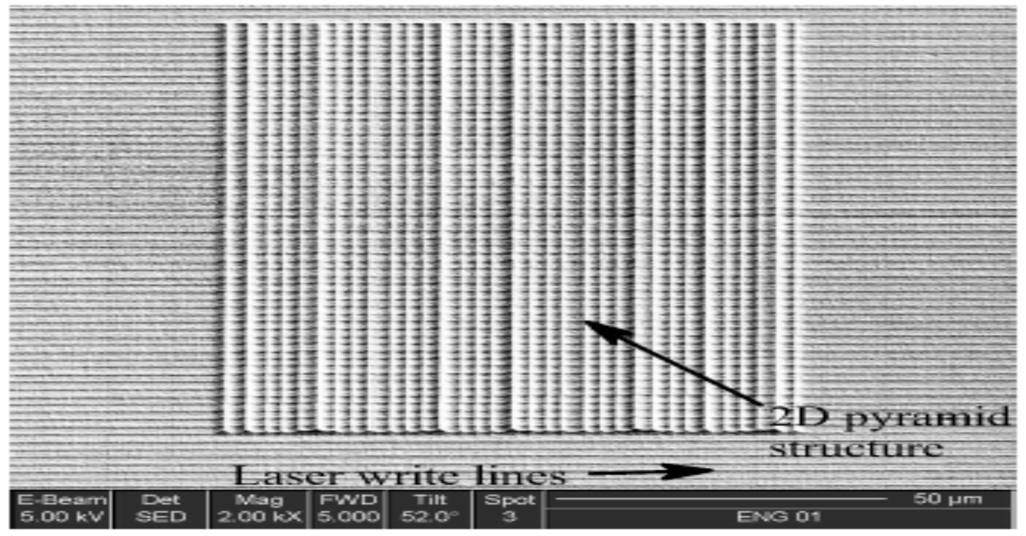
In this work, a Heidelberg µPG-101 system was used to fabricate the 2D pyramid structures used on the bottom contact pads. This system can be operated in two modes: (a) image and (b) line scan. However, both modes have their own limitations, for example, image mode can perform grayscale lithography but offers poor precision. On the other hand, line scan mode offers much higher precision but uses a single power and duty cycle, offering only one level of traditional-type exposure. Therefore, a unique hybrid technique was developed by combining both modes to fabricate 3D structures with higher precision. In this approach, multiple CAD (computer-aided design) designs were superimposed on each other and exposed to low dose UV radiation (in repeated fashion) to achieve the same effect as the bitmap approach, but with much better resolution. Here, only specific information related to 2D pyramid fabrication is given whereas the detailed and more general information about hybrid gray-scale lithography can be found in our previous work [11]. Two different methods were used to fabricate the 2D structures. The first was an image representing the entire die which consisted of 16 beams, and therefore, 16 lower contacts in a 5000 µm × 5000 µm area. This image was scaled to the correct overall size. The second method used the manual alignment of the Heidelberg system to direct where these blocks should be located. This method was more tedious but with the addition of a few alignment marks on the wafer, allowed the precise alignment of the lower contact. A scanning electron microscope image of the final 2D pyramids is shown in Figure 3.

Figure 3.
Scanning electron microscope image of the 2D pyramid design after etching.
3. Results
3.1. Unloaded AC Tests
Figure 4a shows the experimental results of three devices which were tested under cold switch conditions without an external load. These three devices were characterized at three different frequencies and they all failed well before the 10 million cycle goal. The device tested with a 10 kHz signal experienced failure after 2.3 million cycles. On the other hand, the remaining two devices which were tested with 1 kHz and 100 kHz signals both failed before 103 cycles, as shown in Figure 4a. For all three devices, the AC load was comprised of a single cycle applied during the fully closed period of the micro-contact mechanical actuation cycle. In the case of the 1 kHz load, the overall cycle time, at which the contact itself was cycled was limited to 200 Hz, maintained cold-switched conditions. For the 10 kHz load, the testing time was increased to 1 kHz, and for the 100 kHz load, the cycle time was the full 2.5 kHz. These conditions were repeated for all experimental data presented here, but with the addition of external circuit components described in the following sections.
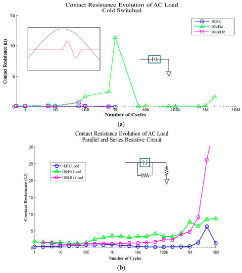
Figure 4.
Contact resistance versus number of cycles measured at three AC frequencies (1, 10 and 100 kHz) for (a) without external load; and (b) with external resistive loaded micro-contacts.
3.2. Performance of Loaded AC Tests
3.2.1. Resistive Load Only
The first external loading configuration was a purely resistive passive load of a 5 MΩ resistor in parallel with the device under test, and a 1 Ω resistor in series. The plotted values of contact resistance shown in Figure 4b do not include the external series resistance. The parallel 5 MΩ resistor had to be included in the measurement with this test configuration to avoid/minimize the in-rush of current for initial closure, but its effects on the measurement were considered negligible. As can be seen from this first set of data, all three devices lasted for 10 million cycles of operation, at which time testing was terminated. In all three cases, similar contact resistance values were observed, and in each case, they remained remarkably stable. Of particular interest was the slight increasing trend in all three cases, but in one case (the 1 kHz device) this resistance dropped back down to normal levels. This resistance correction was similar to the responses shown in DC testing, where irregularities in contact resistance tend to show stabilization with these sorts of passive loads applied.
3.2.2. Resistive-Capacitive-Inductive (RCL) Load
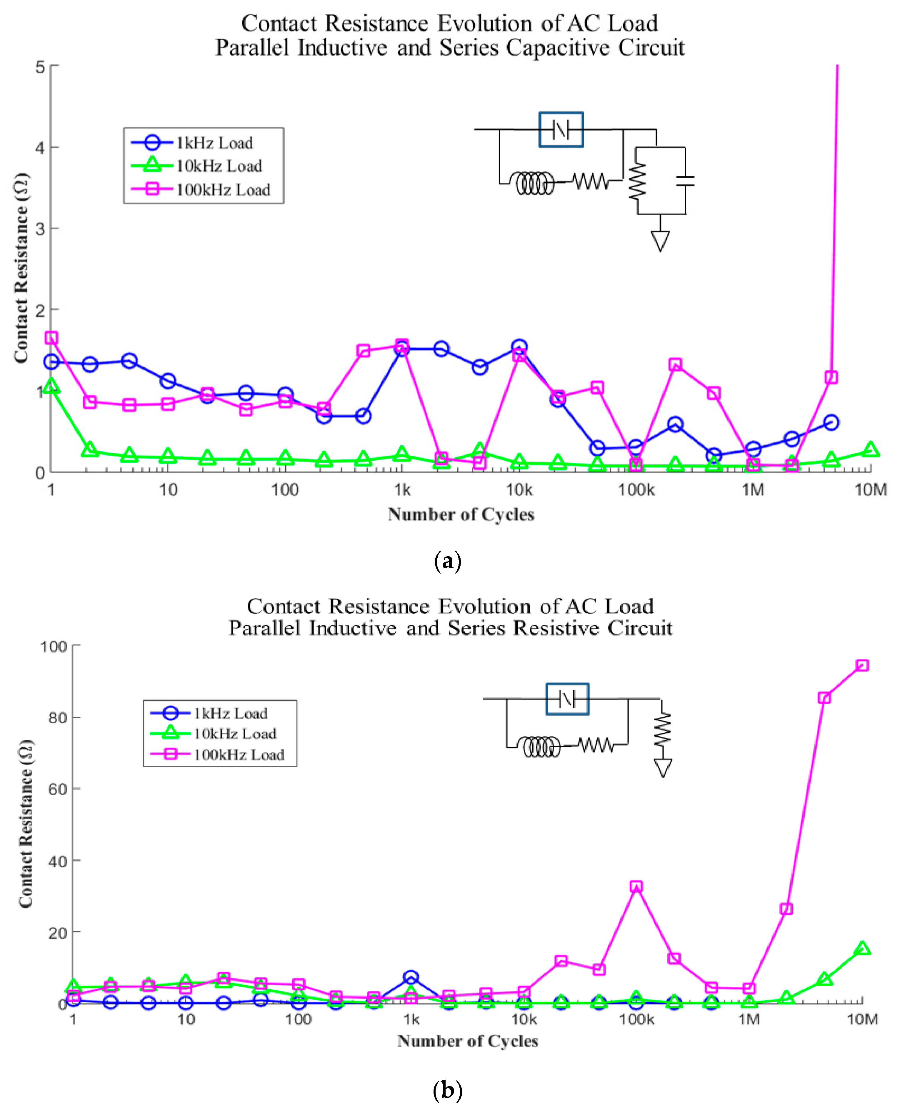
The second loading configuration is shown in Figure 5a. Here, the same resistances were used as in the previous test, but in addition, the parallel resistance had a series inductance added (0.1 µH), and the series resistance was placed in parallel with an additional capacitor (0.6 pF). All other test conditions remained the same as in the previous test. When comparing these results to the previous tests, it is important to note the scale on the plot. While the variability was more erratic than the previous tests, this variance was less than ~2 Ωs throughout the duration of the tests. This circuit configuration resulted in one failed device, which occurred during the 1 kHz AC load test. This failure occurred after ~4.9 million cycles, at which point, the contact failed to open (i.e., shorted). This set of data also includes the most stable result observed from all tests conducted. This occurred with the 10 kHz test, which settled after just a few cycles of operation and remained at roughly 0.25 Ω, even after up to 10 million cycles.
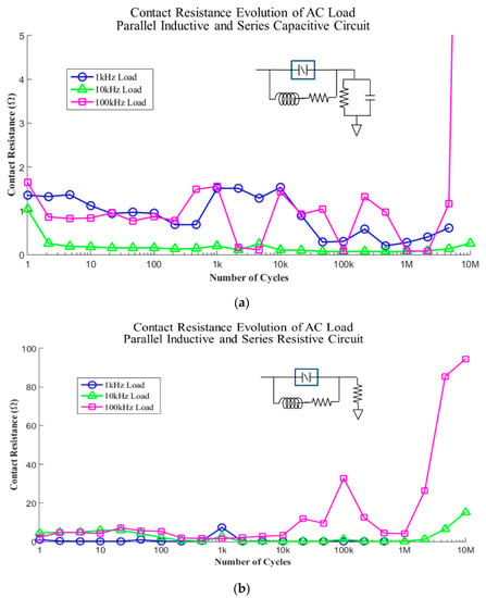
Figure 5.
Contact resistance versus number of cycles measurements at three AC frequencies (1, 10 and 100 kHz) for (a) an external load of parallel resistive-inductive RL and series resistive-capacitive RC; and (b) parallel RL and series resistive (R) added to micro-contacts.
3.2.3. Resistive-Inductive (RL) Load
The third circuit configuration was identical to the second test, but without the capacitance, as shown in Figure 5b. Every other aspect of this test WAs otherwise the same as before. Note that here, we see the second of the two failed devices, which similarly was with the 1 kHz load, and in this case, device failure occurred after ~0.8 million cycles. The two micro-contacts that lasted to 10 million cycles showed the same increased contact resistance near the end of the test as with the purely resistive case (Figure 4a). The100 kHz test showed the high increase in resistance, while the 10 kHz showed the same remarkable stability (<~1 Ω) as it did in Figure 5a.
3.2.4. Resistive-Capacitive (RC) Load
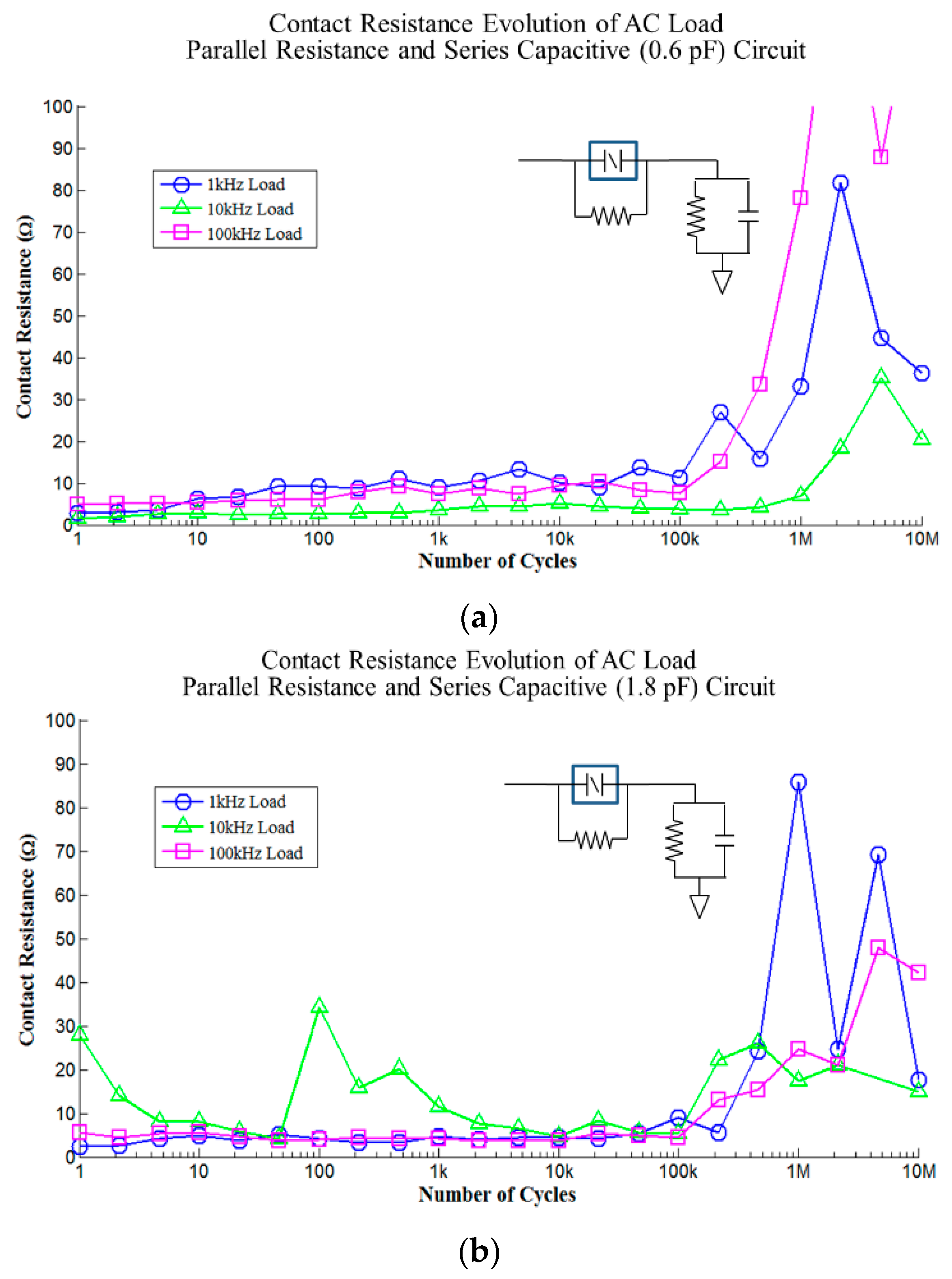
Instead of removing the capacitance from the test structure shown in Figure 5b, the inductance was removed this time. So, in this case, a resistor of 5 MΩ and a parallel combination of 1 Ω resistor and 0.6 pF capacitor were added to the device in parallel and series, respectively. The schematic of this configuration and the test data are shown in Figure 6a. In this test, all three frequencies showed similar results to each other, but they were different from any previous test. It is clear from the plot that the resistance values were larger than the previous experiments and climbed steadily until 105 cycles. Around that point, however, all three devices showed very large increases in contact resistance (i.e., ~few tens of Ω), and in all three cases, there was some level of recovery, but nowhere near back to fully-recovered, stable values. All three devices did, however, last the full 10 million cycles and while their contact resistances were fairly large, the devices were still operational at end of each test.
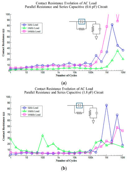
Figure 6.
Contact resistance versus number of cycles measured at three AC frequencies (1, 10 and 100 kHz) for (a) an external load of parallel R and series RC; and (b) parallel R and series RC (larger C this time) added to micro-contacts.
3.2.5. Additional Resistive-Capacitive (RC) Load
The fifth and final set of data was obtained from an identical circuit configuration as the previous test, but the capacitance was tripled (instead of 0.6 pF, a capacitance of 1.8 pF was used). The results of these tests are shown in Figure 6b. The starting resistance of the 10 kHz device tested was ~28 Ω and showed some erratic behavior throughout, but the other two devices tested showed similar overall results to the previous tests. The contact resistance increased and showed more variability past the 105 cycles mark, but the micro-contacts continued to function.
3.3. Comparing the Performance of Micro-Contacts with Different Surface Structures
In the early modeling of contact resistance, the effect of surface contamination was not considered. However, the detrimental effects of surface contamination have been reported for macro-scale mating surfaces which appeared to be smooth but were covered with asperity peaks or ‘a-spots’. These ‘a-spots’ have been described as small, cold welds, providing the only conducting paths for the transfer of electrical current and are the reason for the disparity between the total and effective contact areas. Therefore, the effective area must be used to calculate correct values of RC. The effect of such ‘a-spots’ can be more detrimental to the performance of micro-scale devices which gives the motivation to investigate the micro-contacts of different surface structures.
In addition to planar structures, 2D pyramid structures were also tested in this work. The devices were fabricated using hybrid gray scale lithography, which has already been described in the previous section. Such micro-contacts were also characterized under cold switch conditions to reduce the possibility of electrical failure. For the cold switch program, the micro-contact was first closed before current was applied. With this closed contact, the desired current was applied, and then it was turned off before opening the contact. These steps were then repeated for the desired number of cycles at a maximum frequency of 3 kHz.
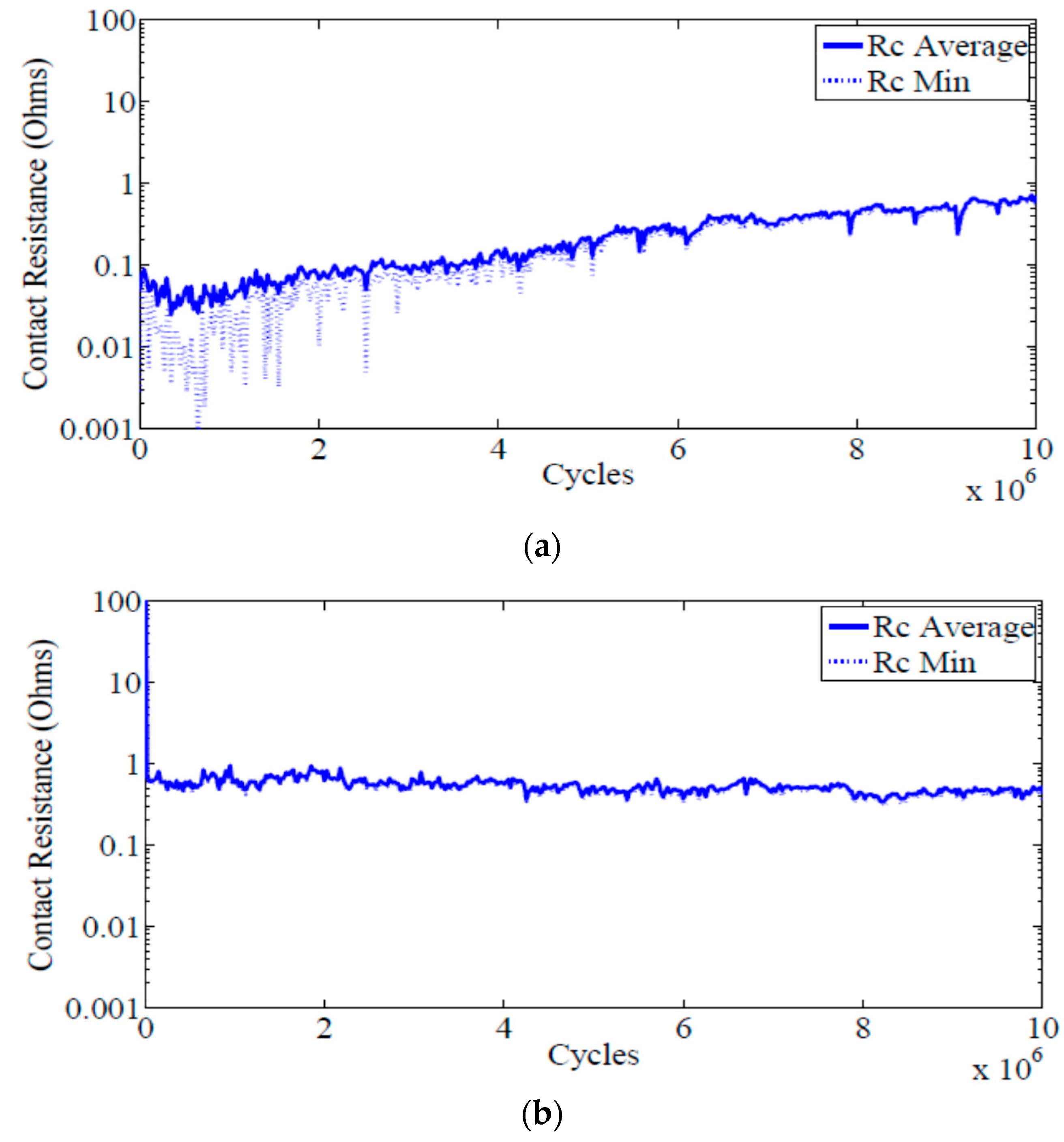
The 107 cycle experiments of all Au–Au micro-contacts were conducted in the same test stand, as shown in Figure 1. The RC plot of the hemispherical-planar micro-contact is shown in Figure 7a.
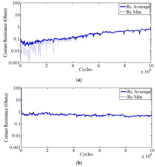
Figure 7.
Contact resistance versus number of cycles measured for (a) planar; and (b) 2D pyramid. For all plots, the contact resistance (RC) average is the average of the last five data points at ~200 µN of contact force, and RC min is the minimum contact resistance measured.
For this case, the average value of RC (~0.1–1.0 Ω) was low throughout testing. However, the value of ‘RC min’ varied within the range of 10−3–1 Ω (variation in ΔRC) which is not desirable for RF application. Similar measurements were performed with hemisphere-2D pyramid micro-contacts, and the results are shown in Figure 7b. Here, the average value of RC (~1 Ω) was slightly higher, but the values of ‘RC min’ were much more stable than the previous planar contact case. Furthermore, unlike the planar contact, the ΔRC was limited to only a few tens of milliohms throughout the lifetime of the micro-contact. All these observations suggest that 2D pyramid structures are superior than planar ones and are potential candidates for transmitting RF signals.
4. Analysis
In our previous work, a theory was proposed to explain the effects of external loads on micro-contact behavior [12]. According to this theory, the presence of transient charge on the contacting surfaces must lead to extremely high current density (particularly at weakened regions) during contact closure which ultimately results in device failure. As this transient charge comes from the capacitive nature of the parallel contacts and associated device layers, any additional ‘C’ in parallel to the device would inadvertently enhance the chances of device failure. Similarly, any ‘L’ in series to the device would also lead to high current density regions developing during a trailing edge hot-switch event, which reduces the lifetime of the device. Therefore, a combination of ‘C’ and ‘L’ loaded to the micro-contact in the correct configuration (C in series and L in parallel) enhances device reliability. In fact, the experimental data from 15 devices presented in this study validates this theory that the correct combination of components significantly improves the micro-contact’s lifetime (under low frequency, low amplitude AC signals) and the incorrect combination reduces the device’s lifetime.
Another important observation is that only two of the 15 devices failed prior to 10 million cycles. Interestingly, both were operated with a 1 kHz load at 200 Hz device cycling frequency and utilized parallel inductance and resistance circuitry. These premature failures were most likely due to the absence of ‘C’ in series. As both components (C and L) contribute to reliability, the absence of either one reduces the device’s lifetime. A second possibility could be the application of a low cycling frequency (200 Hz). At this frequency, the contacts remain closed for a relatively longer period of time which contributes to high current density damaging the device more rapidly. However, if this hypothesis is correct, then all devices operated at 200 Hz cycling frequency should have failed, but that did not happen. The only viable explanation is due to a combined effect of the previous two, i.e., operating the devices at 200 Hz frequency with all ‘L’s, i.e., an external load that does not have any ‘C’ component in series. In this case, the absence of ‘C’ is responsible for the accumulation of transient charges which would generate a large electric field when operated at a low cycling frequency.
The next observation is the relatively higher contact resistance for the devices which were operated at 100 kHz. At higher frequencies, the skin-effect is dominant which reduces the effective contact area (area through which current passes in closure condition) between the top and lower beams and allows the current to pass through the outer region only (and avoids the center). A larger current passing through a smaller area would result in a larger RC.
In comparison to planar contacts, a slightly higher (~1 Ω), but very stable, RC was observed for the micro-contacts with engineered surfaces. Furthermore, this RC was found to decrease a bit near the end of the testing cycle. This behavior could also be demonstrating the concept of the effective contact area. In the engineered 2D lower surfaces, the effective area is reduced due to the presence of a saw-tooth surface structure which results in higher RC than of the for planar contacts. A benefit of this 2D structure is that a specific in-tune RC value can be dialed in ahead of time. In addition, continuous cycling from the top hemisphere “flattens” the pyramid tops which tends to increase the contact area and reduce the RC. At the end, the stability of RC is related to the formation of point contacts between the hemispherical and pyramid structures. The density of such contacts is almost constant for each cycle which gives a nearly identical area throughout the testing time. However, in the hemispherical/planar contact case, asperity peaks were the major source of change in the contact area, resulting in fluctuating RC values. Based on these observations, it is clear that engineered surfaces provide more reliable and stable micro-contacts and when operated under low frequency, low amplitude AC signals with correctly chosen RCL loads, they continue to show improved reliability and performance. The possible failure of hemispherical-2D pyramid contacts occurs when material fills the groves of saw teeth structures and converts them into planar structures. However, this happens after an extended micro-contact lifetime.
5. Conclusions
From these results, several conclusions can be drawn. It is clear that external load components are critical for extending a micro-contact’s lifetime, assuming some level of variability in contact resistance is tolerable. Previous work from which our baseline data were obtained demonstrated 100% failure in all devices prior to reaching 10 million cycles. In this study, those tests were repeated but with the addition of various forms of external loads. Of the 15 devices tested, 13 of those devices reached 10 million cycles and were still operable.
It is also concluded that while this external loading clearly extends the lifetime of the micro-contacts, contact resistance is still being affected. Most of the devices that lasted to 10 million cycles showed a point at which contact resistance began to steadily climb and not show any indication of recovery. Furthermore, large fluctuations and spikes in the RC values of hemispherical-planar contacts demand micro-contacts with modified structures. Here, 2D pyramid structures were fabricated as the lower contact in order to stabilize the RC. This idea worked well as RC was found to be slightly higher but extremely stable compared to the planar lower beam. Overall, the reliability of the micro-contacts under low frequency AC conditions was much improved by engineering the bottom contact surface as well as by properly choosing the external loads. Future work will investigate the combination of external loads and engineered contact surfaces as a means to further enhancing the lifetime of micro-contacts.
Author Contributions
P.M. compiled and edited the final manuscript. R.A.C. conceived the original research idea, proposed the specific project to AFOSR, led the design, fabrication, testing, and data collection efforts, mentored numerous graduate student projects, and edited the final manuscript. D.T. reduced data and provided detailed analysis for the final manuscript.
Acknowledgments
The authors thank Thomas Edleman, Benjamin Toler, Christopher Stilson and Tod V. Laurvick, for their participation in this effort.
Conflicts of Interest
The authors declare no conflict of interest.
References
- Yao, J.J.; Chang, M.F. A surface micromachined miniature switch for telecommunications applications with signal frequencies from DC up to 4 GHz. In Proceedings of the 8th International Conference on Solid-State Sensors and Actuators, 1995 and Eurosensors IX, Stockholm, Sweden, 25–29 June 1995; Volume 2, pp. 384–387. [Google Scholar]
- De Los Santos, H.J.; Kao, Y.H.; Caigoy, A.L.; Ditmars, E.D. Microwave and mechanical considerations in the design of MEM switches for aerospace applications. In Proceedings of the Aerospace Conference, Snowmass, CO, USA, 13 February 1997; Volume 3, pp. 235–254. [Google Scholar]
- Anderson, J.K.; Howell, L.L.; Wittwer, J.W.; McLain, T.W. Piezoresistive sensing of bistable micro mechanism state. J. Micromech. Microeng. 2006, 16, 943. [Google Scholar] [CrossRef]
- Laurvick, T.V.; Coutu, R.A., Jr. Micro-contact Performance and Reliability under low frequency, low amplitude, alternating current (AC) test conditions. In Proceedings of the 2015 IEEE 61st Holm Conference on Electrical Contacts (Holm), San Diego, CA, USA, 11–14 October 2015; pp. 222–226. [Google Scholar]
- Basu, A.; Hennessy, R.P.; Adams, G.G.; McGruer, N.E. Hot switching damage mechanisms in MEMS contacts—Evidence and understanding. J. Micromech. Microeng. 2014, 24, 105004. [Google Scholar] [CrossRef]
- Laurvick, T.V.; Coutu, R.A., Jr. Experimental validation of external load effects on micro-contact performance and reliability. In Proceedings of the 2015 IEEE 61st Holm Conference on Electrical Contacts (Holm), San Diego, CA, USA, 11–14 October 2015; pp. 353–357. [Google Scholar]
- Liu, Y.; Bey, Y.; Liu, X. Extension of the hot-switching reliability of RF-MEMS switches using a series contact protection technique. IEEE Trans. Microw. Theory Tech. 2016, 64, 3151–3162. [Google Scholar] [CrossRef]
- Liu, Y.; Bey, Y.; Liu, X. High-Power High-Isolation RF-MEMS Switches with Enhanced Hot-Switching Reliability Using a Shunt Protection Technique. IEEE Trans. Microw. Theory Tech. 2017, 65, 3188–3199. [Google Scholar] [CrossRef]
- Holm, R. Electric Contacts: Theory and Applications, 4th ed.; Springer: Berlin, Germany, 1967. [Google Scholar]
- Stilson, C.; Laurvick, T.; Coutu, R.A., Jr. Contact resistance evaluation of micro-contacts with upper hemisphere and lower planar or engineered surfaces. In Proceedings of the 2014 IEEE 60th Holm Conference on Electrical Contacts (Holm), New Orleans, LA, USA, 12–15 October 2014; pp. 1–8. [Google Scholar]
- Laurvick, T.; Coutu, R.A., Jr. Improved grayscale lithography. In Proceedings of the 2016 IEEE National Aerospace and Electronics Conference (NAECON) and Ohio Innovation Summit (OIS), Dayton, OH, USA, 25–29 July 2016; pp. 328–332. [Google Scholar]
- Toler, B.; Coutu, R.A., Jr. Characterizing external resistive, inductive and capacitive loads for micro-switches. In MEMS and Nanotechnology; Springer: New York, NY, USA, 2013; Volume 6, pp. 11–18. [Google Scholar]
© 2018 by the authors. Licensee MDPI, Basel, Switzerland. This article is an open access article distributed under the terms and conditions of the Creative Commons Attribution (CC BY) license (http://creativecommons.org/licenses/by/4.0/).

