Abstract
We propose an approach for super-resolution optical lithography which is based on the inverse of magnetic resonance imaging (MRI). The technique uses atomic coherence in an ensemble of spin systems whose final state population can be optically detected. In principle, our method is capable of producing arbitrary one and two dimensional high-resolution patterns with high contrast.
Keywords:
superresolution; subwavelength lithography; NMR imaging; optically detected magnetic resonance PACS:
42.50.St; 76.60.Pc; 76.70.Hb
1. Introduction
Optical lithography is widely used to print circuit images onto substrates because of its inherent parallelism and the fact that its non-ionizing illumination avoids substrate damage. However, the resolution of traditional optical lithography is restricted by the Rayleigh diffraction limit [1,2,3,4]. Due to this limit, we have to use shorter wavelengths such as extreme ultraviolet or X-ray to print smaller patterns [5,6]. However, insulating materials such as silicon dioxide, when exposed to photons with energy greater than the band gap, release free electrons which subsequently can cause adverse charging which can lead to damage [7]. It is therefore interesting and useful to invent an optical lithography scheme that can overcome the diffraction limit.
In the past two decades, a number of methods have been proposed including multiphoton absorption [8,9,10], quantum entanglement [11,12,13], dopperlon [14,15,16], and dark states [17]. However, these methods either require higher order multiphoton absorption, higher order quantum entangled states or multi atomic levels to write patterns with higher order resolution. Thus, improving resolution more than 10 times the optical wavelength with these methods is difficult in practice. In 2010, we proposed a novel scheme to overcome the diffraction limit in optical lithography by inducing Rabi oscillations between two energy levels of the medium [18,19,20]. The extension from lower resolution to higher resolution is straightforward where we just need to increase the power of the excitation laser or the interaction time. However, effectively printing arbitrary one dimensional (1D) and two dimensional (2D) patterns with low background is difficult in this method. Donut beam lithography [21,22],which is the inverse of the ground state depletion (GSD) super-resolution technique [23,24], can write arbitrary patterns with resolution beyond the diffraction limit, but it requires point-by-point scanning instead of full frame exposure and is very inefficient since most of the laser light is actually used to suppress resist exposure. Using frequency-encoded light masks in neutral atom lithography it is possible to print arbitrary sub-diffraction-limited features [25]. However, in atom lithography with very high atom collimation is required for high resolution and this is difficult to achieve with sufficient throughput to be useful for most lithography applications.
In this paper, we propose an approach based on the MRI super-resolution technique [26]. Our method can be conveniently called magnetic resonance lithography (MRL) [27]. This method can be highly parallel, where the parallelism results from the fact that coherent excitation of two-level spin-flip transitions is employed. In this method, the extension from lower resolution to higher resolution is also straightforward where we just need to apply larger magnetic gradient and narrower bandwidth of microwave. Furthermore, it is also possible to print arbitrary 1D and 2D patterns with low background.
This paper is organized as follows. In Section 2, we discuss the basic physics of MRL and propose the pulse sequence to print arbitrary 1D and 2D patterns. In Section 3, we numerically demonstrate how to print an arbitrary 1D and 2D patterns into the spin states and the photoresist. In Section 4, we discuss some possible materials for MRL. Finally, we summarize the results.
2. Basic Principle and Proposed Experiment
MRL requires a paramagnetic system with high spin transition quality factors and high contrast optical readout of the spin state. In addition, to write an arbitrary 2D pattern, the system should have three magnetic sublevels. The proposed schematic setup is shown in Figure 1a where the paramagnetic system is imbeded near the surface of the substrate. We can create the magnetic gradient fields using conductive metal wires fabricated on the substrate surface by means of a conventional photolithography process. The energy levels of the paramagnetic system is shown in Figure 1b. The energy scale of the lower three magnetic sublevels are in the microwave region (1–100 GHz or 5–500 μV ). The energy scale between the ground magnetic sublevels and the higher excited state is in the optical region which is of the order of eV. A static magnetic field is applied from the perpendicular direction to uniformly split the magnetic sublevels and shown in Figure 1b. A microwave pulse with special spectral components is also applied from the perpendicular direction to excite the spin transitions . After preparing the required pattern in the spin states, we may use a laser to excite the spins in state into a fluorescing excited state. A layer of photoresist covers the substrate’s surface to capture the energy from the fluorescing excited state and the spin pattern can then be transfered to the photoresist.
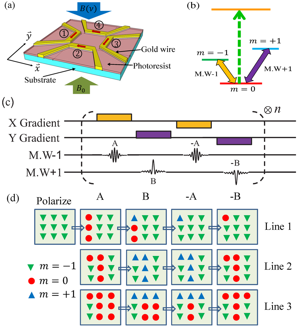
Figure 1.
(Color online) (a) Schematic setup for magnetic resonance lithography. The spins are embedded innear the surface of the substrate. We first write the patterns into the spins and then transfer the spins pattern to the photoresist via the Forster resonance energy transfer, is static magnetic field applied to split the magnetic sublevles while is microwave applied to couple the transition to ; (b) Energy levels for magnetic resonance lithography (MRL). The spin sublevels are coupled by two microwave fields. The green laser is applied to excite the spins to the fluorescence excited state (greed dashed line); (c) The pulse sequence to write an arbitrary 2D binary pattern; (d) An example showing how to write a letter “T” without crosstalk between lines.
To see how MRL can achieve high resolution, let us first consider how to write a narrow line in a spin pattern. If we apply a gradient magnetic field, the Zeeman shift of the sublevels is a function of position. A narrowband microwave π pulse is applied to excite the spins from to one of the sublevels. Only spins with the proper Zeeman shift are resonant with the microwave and the others are not appreciably excited. This is similar to the “resonant z-slice” in MRI [26]. The absolute resolution limit of this technique is given by [28]
where Γ is the spin transition linewidth and is the spatial gradient of Zeeman shift ( in [28] is the spin transition linewidth Γ here and in [28] is the spatial gradient of the Zeeman energy shift in Equation (1)). The width of the line is not limited by the wavelength but by the spin transition linewidth and the gradient of the magnetic field. In principle, we can achieve arbitrary resolution by increasing the gradient of the magnetic field. For example, if the dephasing time is about 10 μs [29] and the gradient of the magnetic field is 100 Gauss/μm, the resolution can be a few nanometers.
We can also address many spatial locations in parallel as in conventional MRI where the narrowband microwave is replaced by a pulse with more complex spectral contents [27]. For example, if we want to print an arbitrary 1D pattern characterized by whose value is normalized into 0 to 1 range, we should have excitation probability given by [30]
where is the pulse duration and is the resonant part of the Rabi frequency seen by atoms at the position x. Here, is the amplitude of the microwave frequency component which is resonant to the transition frequency at position x, is the transition dipole moment between the two relevant energy levels, and ħ is the Planck’s constant. The transition frequency at position x is given by where is the zero field splitting, g MHz/Gauss, and is the magnetic field at position x. The pulse in the time domain is the Fourier transformation of the required spectrum which in turn is related to position because of the magnetic gradient.
2D patterns can also be printed in this setup where all three energy sublevels are involved and both X and Y magnetic gradients should be applied. The proposed pulse sequence is shown in Figure 1c. For example, we want to write a letter “T” (Figure 1d). First, all the spins are polarized to the state (green down triangles). This is the initial state. To write column 1, the X-gradient magnetic field is turned on and a narrowband microwave π pulse (A), whose frequency is tuned to be resonant with spins in column 1, rotates spins in this column from to state. Then the X-gradient is turned off and the Y-gradient is turned on and another microwave pulse (B) with the desired spectrum rotates the spin in the first row from to (blue up triangles) state. To write another column without crosstalk, we need to turn on the negative X-gradient magnetic field again (and turn off the Y-gradient) and then apply the negative of pulse A to rotate unwanted spins (red circle dots) in column 1 back to the state (green down triangles). Finally, we again turn on the negative Y-gradient (with X-gradient off) and the negative of pulse B is applied to rotate the spins in state back to state . A 1D pattern is then formed in the column 1 on the state. After that we can move to the next column and repeat the above procedures. As seen in the figure, the desired 2D pattern “T” can then be encoded in the state. In the ideal case, one spin state such as can be made to fluoresce with excitation laser, while other spin states are dark. An optical readout can then excite the spins in the state into a fluorescing excited state. If the photoresist is within the near-field region of the spins, the fluorescence exposes the photonresist by Föster resonance energy transfer (FRET) [31,32]. To avoid the direct exposure of the photo-resist by the excitation light, we require that the paramagnetic material has quite different absorption and emission frequency bandwidth. For example the negatively charged Nitrogen Vacancy (NV) color center in diamond can be excited by a green light but emit a red light. We can then choose a photo-resist that is only sensitive at the wavelength of the emission light but not sensitive at the wavelength of the excitation light. Usually, the absorption band of a photoresist is determined by the photoinitiator. With commercially available photoinitiators, it is possible to formulate a photoresist that is only sensitive to a narrowband of the optical spectrum, for example the H-Nu Blue 640 and 660 which is red but not green sensitive [33].
The FRET efficiency is given by , where is the critical FRET radius and R is the distance between the emitter and the receiver. To capture the high resolution features of the patteren, the photoresist needs to be within the FRET radius from the paramagnetic system. This could be achieved in several ways depending on the nature of the paramagnetic system. For example, for paramagnetic defects in crystals, this could be achieved by shallow implantation or engineered growth techniques. A more practical approach, however, would be to coat the substrate surface with a photoresist that contains paramagnetic molecules or nanoparticles with paramagnetic defects. In this way, patterns with higher aspect ratio can be achieved.
3. Numerical Simulation
In the following, we apply a numerical simulation to write a 1D and a 2D pattern onto the state using MRL. The dynamics of the system is govern by the master equation
where ρ is density matrix for the three energy sub-levels, H is the Hamiltonian given by with being the Rabi frequency of the transition, being the corresponding detuning, being the Rabi frequency of the transition and being the corresponding detuning. Here, is determined by the X(Y) gradient magnetic field, and is determined by the microwave pulse A(B). The last term is the dephasing of the system. The whole process needs to be done before the population decay time which can be of the order of milliseconds. Here, we neglect population decay but keep the dephasing process. In the numerical simulation, we apply the Fourth-Order Runge-Kutta method to solve the time evolution of Equation (3) with Rabi frequencies and detunings vary as the pulse sequence shown in Figure 1c.
For the 1D pattern example, we write a chirped grating within a 150 nm field of view using numerical simulation. Here, only an X-gradient and the transition are involved. The spins are initially prepared in state. We assume the wire diameter is 1 μm and the distance between the centers of the two wires is 2 . The currents in both wires are 50 mA and in the same direction. The currents generate a magnetic gradient of about 200 Gauss/μm in the X-direction. The magnetic field envelope of the microwave excitation pulse for the transition in the time domain is shown in Figure 2a. The total time duration is about 20 μs. This desired pulse could be generated with a commercial arbitrary waveform generator (AWG). Using an AWG also allows any non-uniformities in magnetic bias or gradient fields to be compensated by applying the appropriate inverse non-linearity to the AWG instruction set. In the numerical simulation, we assume the Rabi frequency has amplitude fluctuation. The paramagnetic material is assumed to be 5 nm deep. The probability that the spins are in the state is shown in Figure 2b where we can see that the desired pattern is encoded in the bright state. The pattern of the internal state can then be transfered to the photoresist by the FRET. The FRET efficiency on the substrate surface is shown in Figure 2c where is assumed to be . We can see that a chirped grating can be generated with very high contrast (It is noted that the efficiency presented in Figure 2c can be greater than 1 because it is the summation of the FRET efficiencies of multiple emitters).
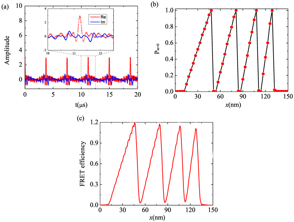
Figure 2.
(Color online) (a) Complex RF pulse used to write a chirped grating. Red line with cross symbols is the real part while blue line without symbols is the imaginary part; (b) The spatial distribution of the probability that the spins are prepared in the bright state; (c) The Föster resonance energy transfer (FRET) efficiency on the substrate surface when the readout contrast is .
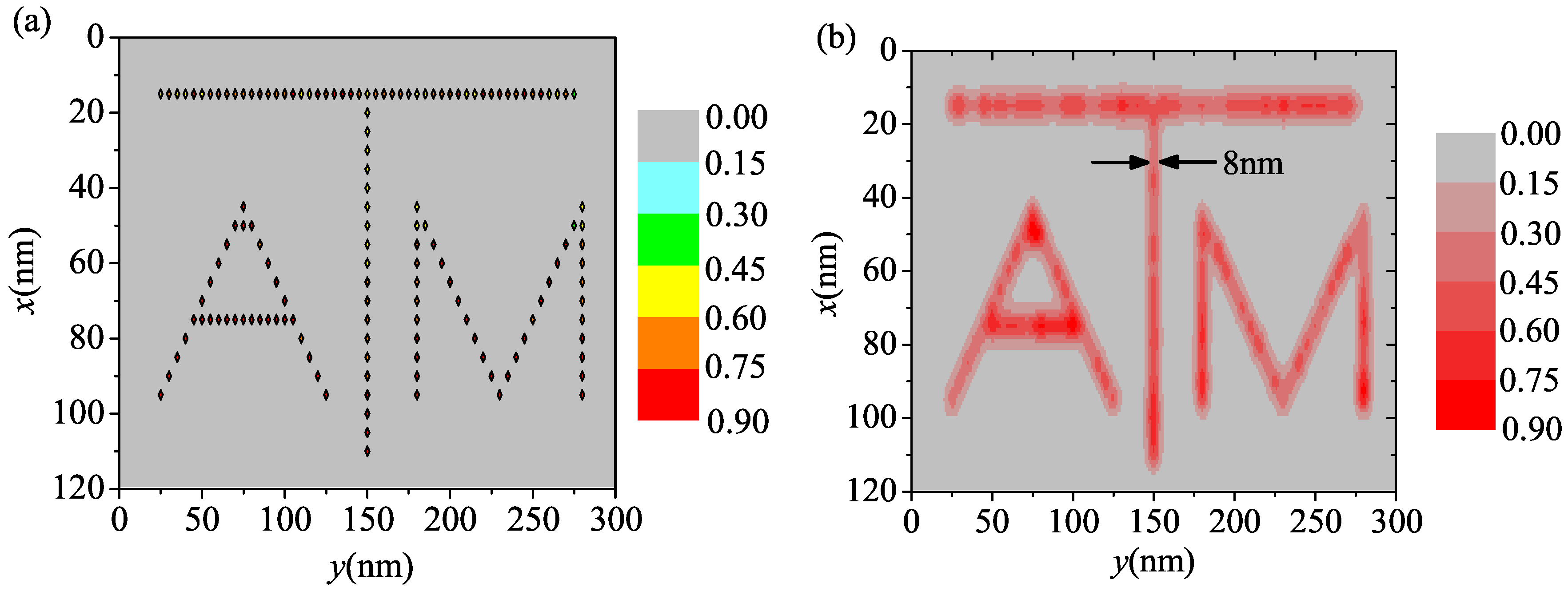
For a 2D pattern numerical example, we write the Texas A&M University logo (“ATM”) into a 120 nm × 300 nm region. This area is divided into 24 slices in the x direction and 60 slices in the y direction. The separation of the spins is chosen to be 5 nm on a square grid. The implantation of square grid of spin defects may be generated by electron holography lithography [34] or nano-sphere lithography [35]. The pulse sequence is shown in Figure 1d where both X-gradient and Y-gradient magnetic fields are involved. In the numerical simulation, the gradients in both directions are generated by 100 mA currents using the same wire separation as in the 1D example. The narrow band microwave π pulse used to drive transitions is assumed to have a Gaussian time envelope. The time duration of the entire pulse A which selects a line is about 2.7 μs where the Gaussian envelope portion has a width of about 0.75 μs. The time duration of the complex pulse B is also about 2.7 μs which is discretized into 5000 time steps. The total time duration to write one line is about 10.8 μs and it is about 250 μs for the whole process. The dephasing time is assumed to be about 20 μs [36]. Again, the amplitudes of the pulses have a fluctuation of about . The probability that the spins are in the bright state () is shown in Figure 3a where we can see that the desired pattern is successfully encoded into the internal state of the system. Finally, an optical readout can transfer the pattern of the internal states to the photoresist. Assuming that the paramagnetic spins are about 5 nm deep with 1 nm uncertainty and the FRET radius is 5 nm, the relative FRET efficiency at the surface is shown in Figure 3b where we see that the desired pattern can be formed. The full width at half maximum of the line in the middle is about 8 nm.
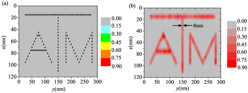
Figure 3.
(Color online) Numerical simulation to write the Texas A&M University logo into a two-dimensional area using MRL. (a) The spatial distribution of the probability that the spins are prepared in the bright state; (b) The FRET efficiency on the substrate surface when the readout contrast is .
4. Possible materials for MRL
As is mentioned in Sec. II, MRL requires a solid system with high spin transition quality factors and high contrast optical readout of the spin state. There are a number of possible systems which can satisfy these requirements. One promising candidate is the negativley charged NV color center in diamond. The NV exhibits an optically detected magnetic resonance (ODMR) spin system with long coherence times, even at room temperature [37,38,39,40]. Coherence times larger than a millisecond have been experimentally achieved for NVs leading to their frequent use as nanoscale magnetic field sensors [40]. Such properties could give MRL resolutions as high as a few nanometers. Unfortunately at room temperature the optical readout of the NV spin state has less than contrast. Nonetheless, the inherent nonlinearity of resist exposure may allow us to produce high contrast patterns, even with this relatively low optical contrast.
One alternative candidate is the silicon vacancy (SiV) center in diamond. The SiV has an optical readout contrast near at low temperature since its ground state sublevel transitions can be optically resolved [41]. Unlike NV and many other materials, this high resolution persists even for ensembles, due to the low inhomogeneous broadening and low spectral diffusion of SiV. Granted that working at low temperature might produce some technical difficulties; nonetheless, photoresist exposure has been demonstrated in cryogenic temperatures [42]. Another important advantage of the SiV is that it can have optical Raman transitions connecting the ground state sublevels. Here, light shift gradients could also replace magnetic field gradients [43] so that no wires would be needed on the substrate at all.
Finally, we briefly consider other possible materials systems for performing MRL at room temperature. One of these is the ST1 color center exhibiting a high optical readout contrast up to , albeit with shorter spin lifetimes [44]. Ruby is also of interest as it has shown room temperature optical Raman transitions with readout contrast comparable to NV [45]. Other alternatives are the rare-earth doped materials. For instance, super-resolution microscopy has been demonstrated using praseodymium-doped yttrium aluminum garnet (Pr:YAG) at room temperature [46]. The upconversion UV emission of (Pr:YAG) is optimal for photoresist exposure. Hence, the prospects are good that a material suitable for room temperature MRL will eventually be identified.
5. Summary
In summary, we have proposed an approach to achieve super-resolution in the optical lithography. This technique is based on the inverse of magnetic resonance imaging. The resolution is not limited by the wavelength of the microwave or the light source but depends on the spin transition linewidth and the maximum gradient of the magnetic field. We design a pulse sequence to write arbitrary 1D and 2D patterns into the spin states with very high resolution. The spin patterns may then be optically detected and transferred to the photoresist pattern by the FRET. We presented a numerical simulation to prove the fundamental physics of MRL which shows that our method is capable of producing arbitrary 1D and 2D high-resolution patterns in one of the spin sublevels with high contrast. We may also further improve the performance of our scheme by designing an echo sequence to eliminate the pure dephasing effect and narrow the spin transition linewidth from to . Finally, we propose several possible paramagnetic materials for MRL which may be experimentally implemented in the future. The realization of our technique could find important applications in the semiconductor industry.
Acknowledgments
This work is supported by grants from the Qatar National Research Fund (QNRF) under the NPRP project 8-352-1-074 and the King Abdulaziz City for Science and Technology (KACST), DARPA QuASAR, and NSF 1202258. We acknowledge helpful discussions with Charles Santori of HP Laboratories.
Author Contributions
Philip Hemmer and M. Suhail Zubairy conceived the study. Fahad AlGhannam, Philip Hemmer, and Zeyang Liao designed the pulse sequences and performed the numerical simulations. All authors contributed to the basic theory and the manuscript preparation. All authors have read and approved the final manuscript.
Conflicts of Interest
The authors declare no conflict of interest.
Abbreviations
The following abbreviations are used in this manuscript:
| MRI | Magnetic resonance imaging |
| MRL | Magnetic resonance lithography |
| GSD | Ground state depletion |
| FRET | Föster resonance energy transfer |
| AWG | Arbitray waveform generator |
| NV | Nitrogen Vacancy |
| ODMR | Optically detected magnetic resonance |
| SiV | Silicon Vacancy |
| Pr:YAG | Praseodymium-doped yttrium aluminum garnet |
References
- Rayleigh, L. Investigations in Optics, with Special Reference to the Spectroscope. Philos. Mag. Ser. 1880, 9, 40–55. [Google Scholar] [CrossRef]
- Abbe, E. Beitrge zur Theorie des Mikroskops und der Mikroskopischen. Arch. Mikr. Anat. 1873, 9, 413–418. [Google Scholar] [CrossRef]
- Al-Amri, M.; Liao, Z.; Zubairy, M.S. Beyond the Rayleigh Limit in optical Lithography. In Advances in Atomic, Molecular, and Optical Physics; Arimondo, E., Berman, P.R., Lin, C.C., Eds.; Academic Press: Cambridge, MA, USA, 2012; Volume 61, pp. 409–466. [Google Scholar]
- Hemmer, P.R.; Zapata, T. The universal scaling laws that determine the achievable resolution in diffraction schemes for super-resolution imaging. J. Opt. 2012, 14, 083002. [Google Scholar] [CrossRef]
- Gwyn, C.W.; Stulen, R.; Sweeney, D.; Attwood, D. Extreme ultraviolet lithography. J. Vac. Sci. Technol. B 1998, 16, 3142–3149. [Google Scholar] [CrossRef]
- Heuberger, A. X-ray lithography. J. Vac. Sci. Technol. B 1988, 6, 107–121. [Google Scholar] [CrossRef]
- Williams, C.; Kok, P.; Lee, H.; Dowling, J.P. Quantum lithography: A non-computing application of quantum information. Inform. Forsch. Entw. 2006, 21, 73–82. [Google Scholar] [CrossRef]
- Yablonovitch, E.; Vrijen, R.B. Optical Projection Lithography at Half the Rayleigh Resolution Limit by Two-photon Exposure. Opt. Eng. 1999, 38, 334–338. [Google Scholar] [CrossRef]
- Pe’er, A.; Dayan, B.; Vucelja, M.; Silberberg, Y.; Friesem, A.A. Quantum lithography by coherent control of classical light pulses. Opt. Express 2014, 12, 6600–6605. [Google Scholar] [CrossRef]
- Bentley, S.J.; Boyd, R.W. Nonlinear optical lithography with ultra-high sub-Rayleigh resolution. Opt. Express 2004, 12, 5735–5740. [Google Scholar] [CrossRef] [PubMed]
- Boto, A.N.; Kok, P.; Abrams, D.S.; Braunstein, S.L.; Williams, C.P.; Dowling, J.P. Quantum interferometric optical lithography: Exploiting entanglement to beat the diffraction limit. Phys. Rev. Lett. 2000, 85. [Google Scholar] [CrossRef] [PubMed]
- D’Angelo, M.; Chekhova, M.V.; Shih, Y. Two-Photon Diffraction and Quantum Lithography. Phys. Rev. Lett. 2001, 87, 013602. [Google Scholar] [CrossRef] [PubMed]
- Agarwal, G.S.; Boyd, R.W.; Nagasako, E.M.; Bentley, S.J. Quantum interferometric optical lithography: Exploiting entanglement to beat the diffraction limit. Phys. Rev. Lett. 2001, 86, 1389. [Google Scholar] [CrossRef] [PubMed]
- Hemmer, P.R.; Muthukrishnan, A.; Scully, M.O.; Zubairy, M.S. Quantum lithography with classical light. Phys. Rev. Lett. 2006, 96, 163603. [Google Scholar] [CrossRef] [PubMed]
- Sun, Q.; Hemmer, P.R.; Zubairy, M.S. Quantum lithography with classical light: Generation of arbitrary patterns. Phys. Rev. A 2007, 75, 065803. [Google Scholar] [CrossRef]
- Ge, W.; Hemmer, P.R.; Zubairy, M.S. Quantum lithography with classical light. Phys. Rev. A 2013, 87, 023818. [Google Scholar] [CrossRef]
- Kiffner, M.; Evers, J.; Zubairy, M.S. Resonant Interferometric Lithography Beyond the Diffraction Limit. Phys. Rev. Lett. 2008, 100, 073602. [Google Scholar] [CrossRef] [PubMed]
- Liao, Z.; Al-Amri, M.; Zubairy, M.S. Quantum Lithography beyond the Diffraction Limit via Rabi Oscillations. Phys. Rev. Lett. 2010, 105, 183601. [Google Scholar] [CrossRef] [PubMed]
- Liao, Z.; Al-Amri, M.; Becker, T.; Schleich, W.P.; Scully, M.O.; Zubairy, M.S. Atomic Lithography with Subwavelength Resolution via Rabi Oscillations. Phys. Rev. A 2013, 87, 023405. [Google Scholar] [CrossRef]
- Liao, Z.; Al-Amri, M.; Zubairy, M.S. Coherent Atom Lithography with Nanometer Spacing. Phys. Rev. A. 2013, 88, 053809. [Google Scholar] [CrossRef]
- Brimhall, N.; Andrew, T.L.; Manthena, R.V.; Menon, R. Breaking the Far-Field Diffraction Limit in Optical Nanopatterning via Repeated Photochemical and Electrochemical Transitions in Photochromic Molecules. Phys. Rev. Lett. 2011, 107, 205501. [Google Scholar] [CrossRef] [PubMed]
- Gan, Z.; Cao, Y.; Evans, R.A.; Gu, M. Three-dimensional deep sub-diffraction optical beam lithography with 9 nm feature size. Nat. Commun. 2013, 4. [Google Scholar] [CrossRef] [PubMed]
- Hell, S.W.; Wichmann, J. Breaking the diffraction resolution limit by stimulated emission: Stimulated-emission-depletion fluorescence microscopy. Opt. Lett. 1994, 19, 780–782. [Google Scholar] [CrossRef] [PubMed]
- Hell, S.W.; Kroug, M. Ground-state-depletion fluorscence microscopy: A concept for breaking the diffraction resolution limit. Appl. Phys. B Lasers Optics 1995, 60, 495–497. [Google Scholar] [CrossRef]
- Thywissen, J.H.; Prentiss, M. Demonstration of frequency encoding in neutral atom lithography. New J. Phys. 2005, 7. [Google Scholar] [CrossRef]
- Haacke, E.M.; Brown, R.W.; Thompson, M.R.; Venkatesan, R. Magnetic Resonance Imaging: Physical Principles and Sequence Design; John Wiley and Sons: New York, NY, USA, 1999. [Google Scholar]
- Hemmer, P.; AlGhannam, F.; Zubairy, M.S. Toward sub-wavelength lithography with atomic coherence. Proc. SPIE 2013, 8875. [Google Scholar] [CrossRef]
- McFarland, E.W. Time-independent point-spread function for NMR microscopy. Magn. Reson. Imaging 1992, 10, 269–278. [Google Scholar] [CrossRef]
- Ofori-Okai, B.K.; Pezzagna, S.; Chang, K.; Loretz, M.; Schirhagl, R.; Tao, Y.; Moores, B.A.; Groot-Berning, K.; Meijer, J.; Degen, C.L. Spin properties of very shallow nitrogen vacancy defects in diamond. Phys. Rev. B 2012, 86, 081406. [Google Scholar] [CrossRef]
- Scully, M.O.; Zubairy, M.S. Quantum Optics; Cambridge University Press: Cambridge, UK, 1997. [Google Scholar]
- Clegg, R.M. Laboratory Techniques in Biochemistry and Molecular Biology; Gadella, T.W.J., Ed.; Elsevier: Amsterdam, The Netherlands, 2009; Volume 33, pp. 1–57. [Google Scholar]
- Tisler, J.; Reuter, R.; Lämmle, A.; Jelezko, F.; Balasubramanian, G.; Hemmer, P.R.; Reinhard, F.; Wrachtrup, J. Highly Efficient FRET from a Single Nitrogen-Vacancy Center in Nanodiamonds to a Single Organic Molecule. ACS Nano 2011, 5, 7893–7898. [Google Scholar] [CrossRef] [PubMed]
- Spectra Group Limited Inc. H-Nu Blue 640, 660 Visible Light Photoinitiators. Available online: http://www.sglinc.com/Portals/0/Images/limited/PDFS/photoinitiators/H-Nu20Blue-IR20TDS.pdf (accessed on 20 April 2012).
- Dunin-Borkowski, R.E.; Kasama, T.; Wei, A.; Tripp, S.L.; Hytch, M.J.; Snoeck, E.; Harrison, R.J.; Putnis, A. Off-axis electron holography of magnetic nanowires and chains, rings, and planar arrays of magnetic nanoparticles. Microsc. Res. Tech. 2004, 64, 390–402. [Google Scholar] [CrossRef] [PubMed]
- Cheung, C.L.; Nikolić, R.J.; Reinhardt, C.E.; Wang, T.F. Fabrication of nanopillars by nanosphere lithography. Nanotechnology 2006, 17. [Google Scholar] [CrossRef]
- Ohno, K.; Heremans, F.J.; Bassett, L.C.; Myers, B.A.; Toyli, D.M.; Bleszynski Jayich, A.C.; Palmstrøm, C.J.; Awschalom, D.D. Engineering shallow spins in diamond with nitrogen delta-doping. Appl. Phys. Lett. 2012, 101, 082413. [Google Scholar] [CrossRef]
- Gaebel, T.; Domhan, M.; Popa, I.; Wittmann, C.; Neumann, P.; Jelezko, F.; Rabeau, J.R.; Stavrias, N.; Greentree, A.D.; Prawer, S.; et al. Room-temperature coherent coupling of single spins in diamond. Nat. Phys. 2006, 2, 408–413. [Google Scholar] [CrossRef]
- Childress, L.; Gurudev Dutt, M.V.; Taylor, J.M.; Zibrov, A.S.; Jelezko, F.; Wrachtrup, J.; Hemmer, P.R.; Lukin, M.D. Coherent Dynamics of Coupled Electron and Nuclear Spin Qubits in Diamond. Science 2006, 314, 281–285. [Google Scholar] [CrossRef] [PubMed]
- Wrachtrup, J.; Jelezko, F. Processing quantum information in diamond. J. Phys. Condens. Matter 2006, 18. [Google Scholar] [CrossRef]
- Balasubramanian, G.; Neumann, P.; Twitchen, D.; Markham, M.; Kolesov, R.; Mizuochi, N.; Isoya, J.; Achard, J.; Beck, J.; Tissler, J.; et al. Ultralong spin coherence time in isotopically engineered diamond. Nat. Matter 2009, 8, 383–387. [Google Scholar] [CrossRef] [PubMed]
- Müller, T.; Hepp, C.; Pingault, B.; Neu, E.; Gsell, S.; Schreck, M.; Sternschulte, H.; Steinmller-Nethl, D.; Becher, C.; Atatüre, M. Optical signatures of silicon-vacancy spins in diamond. Nat. Commun. 2014, 5. [Google Scholar] [CrossRef] [PubMed]
- Lee, K.H.; Green, A.M.; Taylor, R.A.; Sharp, D.N.; Turberfield, A.J.; Brossard, F.S.F.; Williams, D.A.; Briggs, G.A.D. Cryogenic two-photon laser photolithography with SU-8. Appl. Phys. Lett. 2006, 88, 143123. [Google Scholar] [CrossRef]
- Gardner, J.R.; Marable, M.L.; Welch, G.R.; Thomas, J.E. Suboptical wavelength position measurement of moving atoms using optical fields. Phys. Rev. Lett. 1993, 70. [Google Scholar] [CrossRef] [PubMed]
- Lee, S.-Y.; Widmann, M.; Rendler, T.; Doherty, M.W.; Babinec, T.M.; Yang, S.; Eyer, M.; Siyushev, P.; Hausmann, B.J.M.; Loncar, M.; et al. Readout and control of a single nuclear spin with a metastable electron spin ancilla. Nat. Nanotechnol. 2013, 8, 487–492. [Google Scholar] [CrossRef] [PubMed]
- Kolesov, R. Coherent population trapping in a crystalline solid at room temperature. Phys. Rev. A 2005, 72, 051801. [Google Scholar] [CrossRef]
- Kolesov, R.; Reuter, R.; Xia, K.; Stöhr, R.; Zappe, A.; Wrachtrup, J. Super-resolution upconversion microscopy of praseodymium-doped yttrium aluminum garnet nanoparticles. Phys. Rev. B 2011, 84, 153413. [Google Scholar] [CrossRef]


© 2016 by the authors; licensee MDPI, Basel, Switzerland. This article is an open access article distributed under the terms and conditions of the Creative Commons Attribution (CC-BY) license (http://creativecommons.org/licenses/by/4.0/).