Investigation of Phase Segregation in Highly Doped InP by Selective Electrochemical Etching
Abstract
1. Introduction
2. Materials and Methods
2.1. Materials
2.2. Electrochemical Cell and Electrodes
2.3. Etching Solutions
2.4. Control Modes, Voltage/Current, and I(t) Recording
2.5. Post-Treatment of Samples
2.6. Electron Microscopy
3. Results
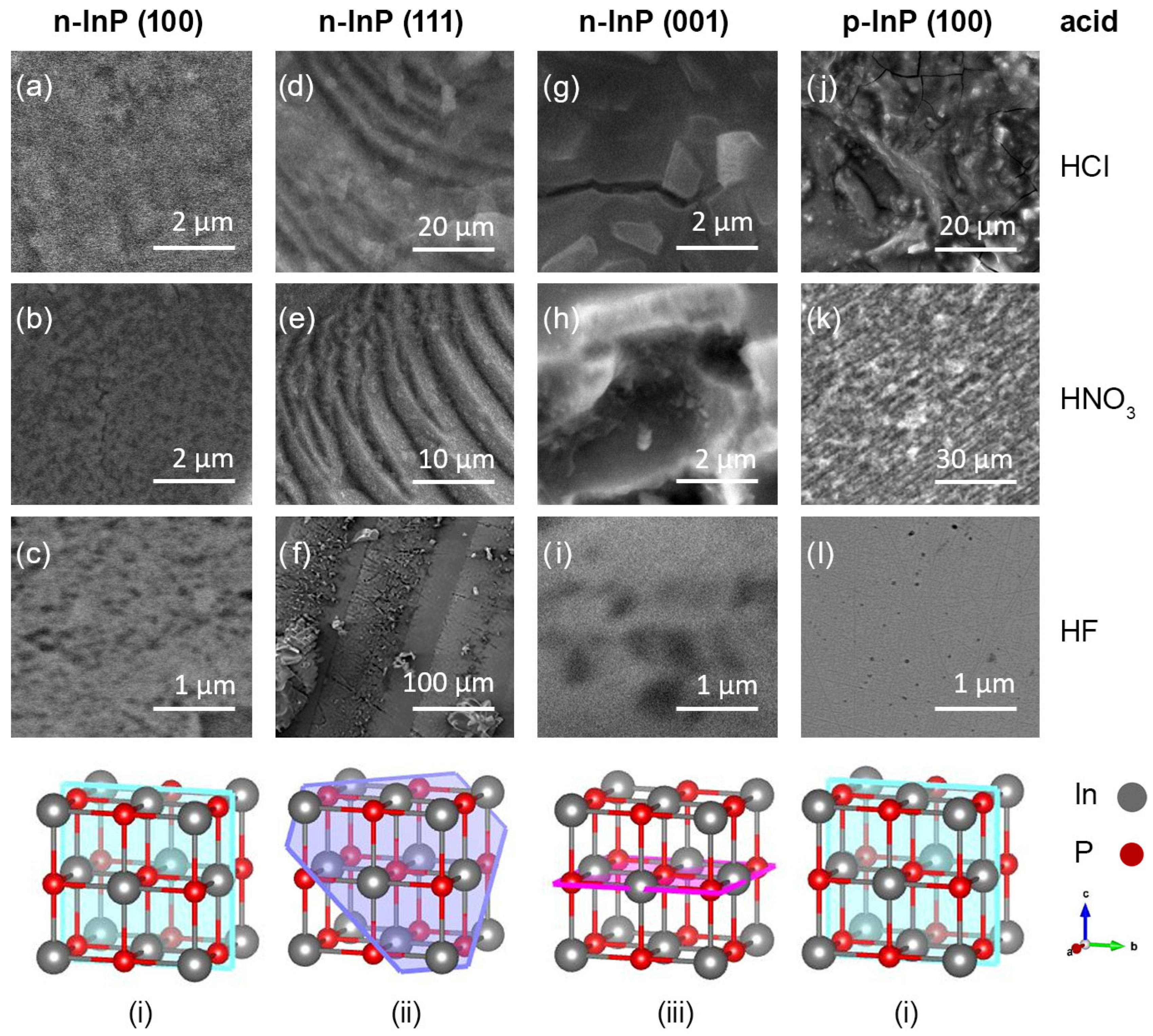
3.1. Investigation of Etch Pits on the Surface of InP with Different Crystallographic Orientations
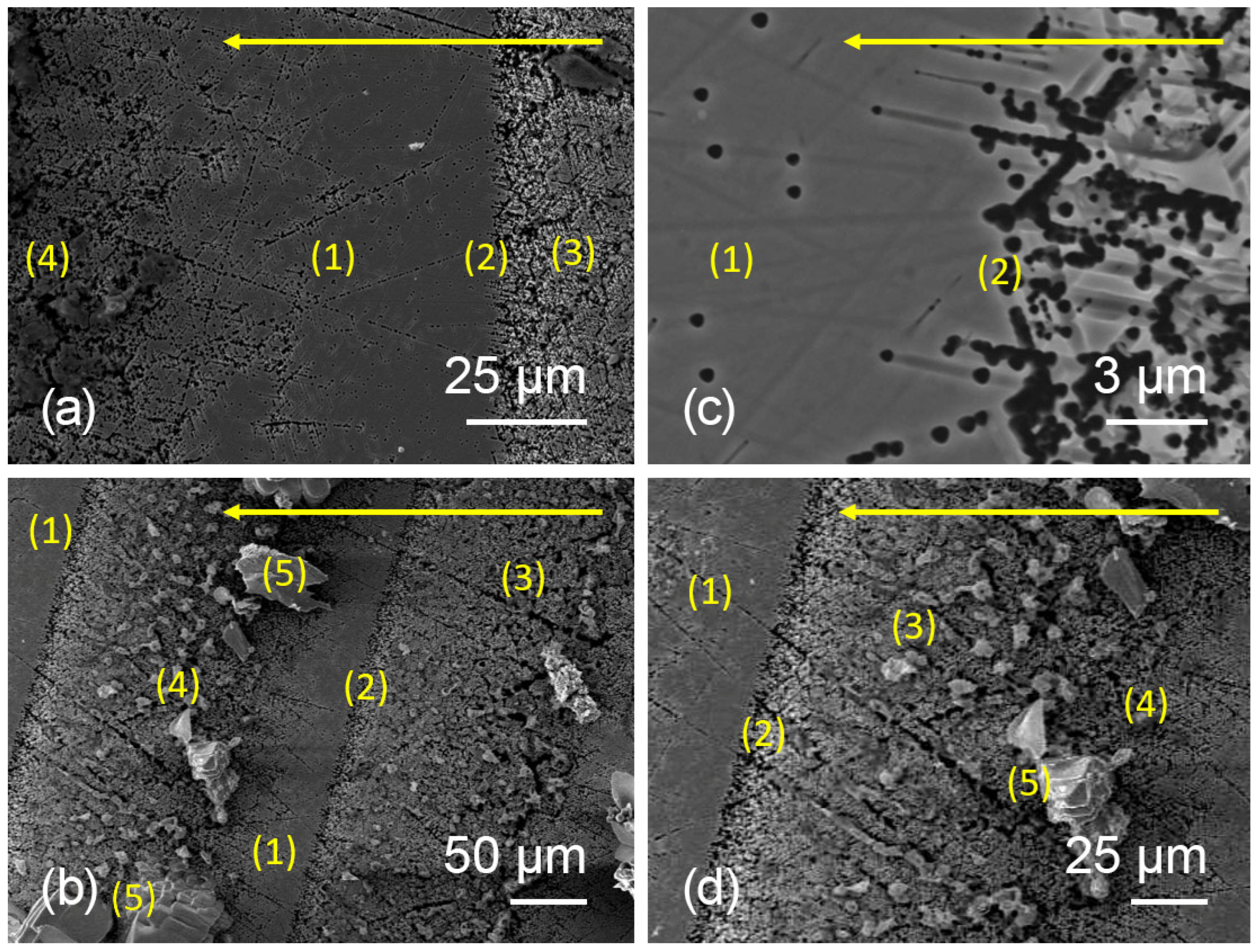
3.2. Formation of Growth Defects in InP During Czochralski Method Growth
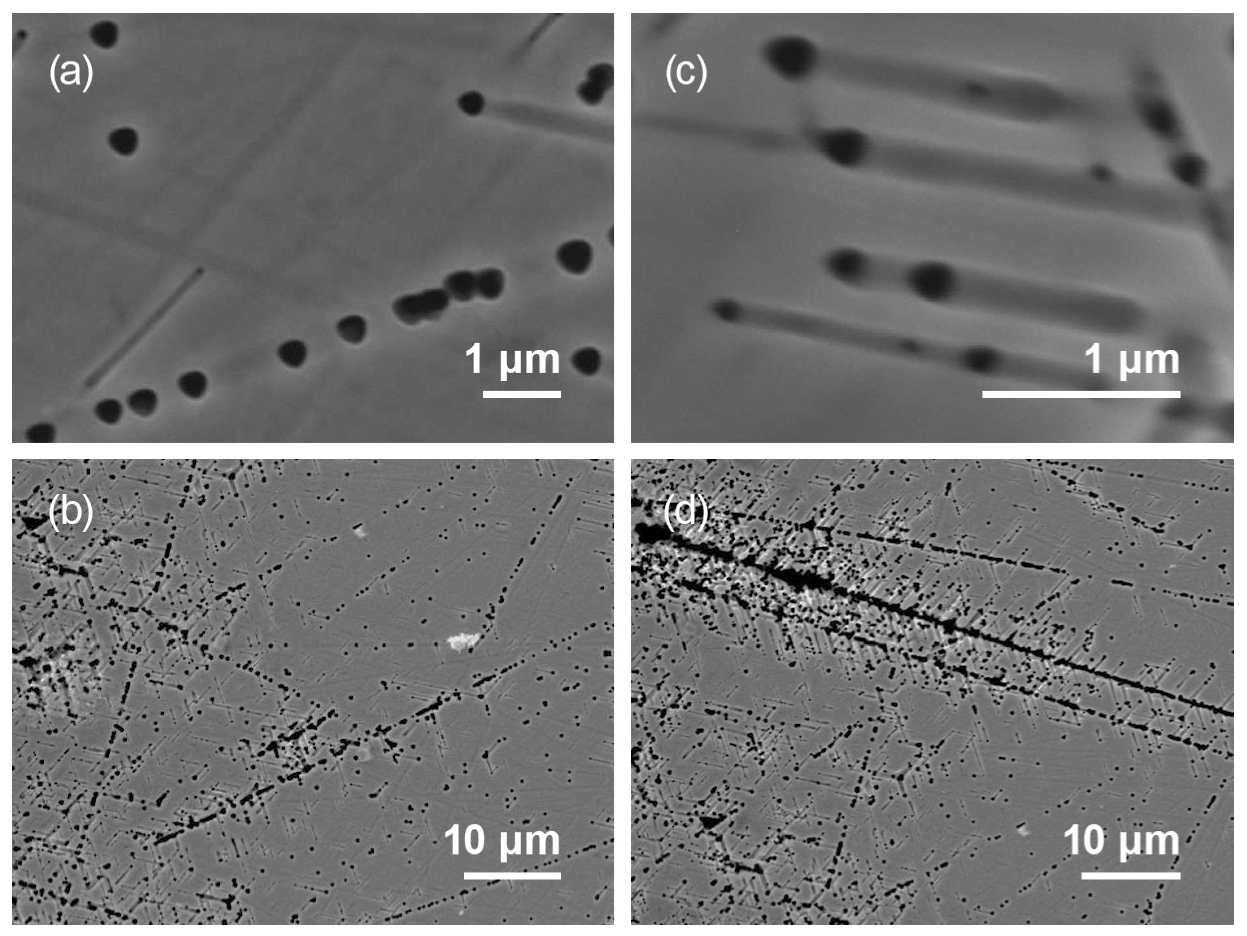
3.3. Investigation of Etch Pits Along Dislocation Slip Lines
3.4. Formation of Oxide Crystallites at Sites of Accumulation of Defects in the Crystal Lattice
4. Discussion
4.1. Mechanism 1: Phase Segregation During Czochralski Growth
4.2. Mechanism 2: Dislocation Dynamics and Their Influence on Defect Formation
4.3. Mechanism 3: Electrochemical Etching and Anisotropic Surface Morphology
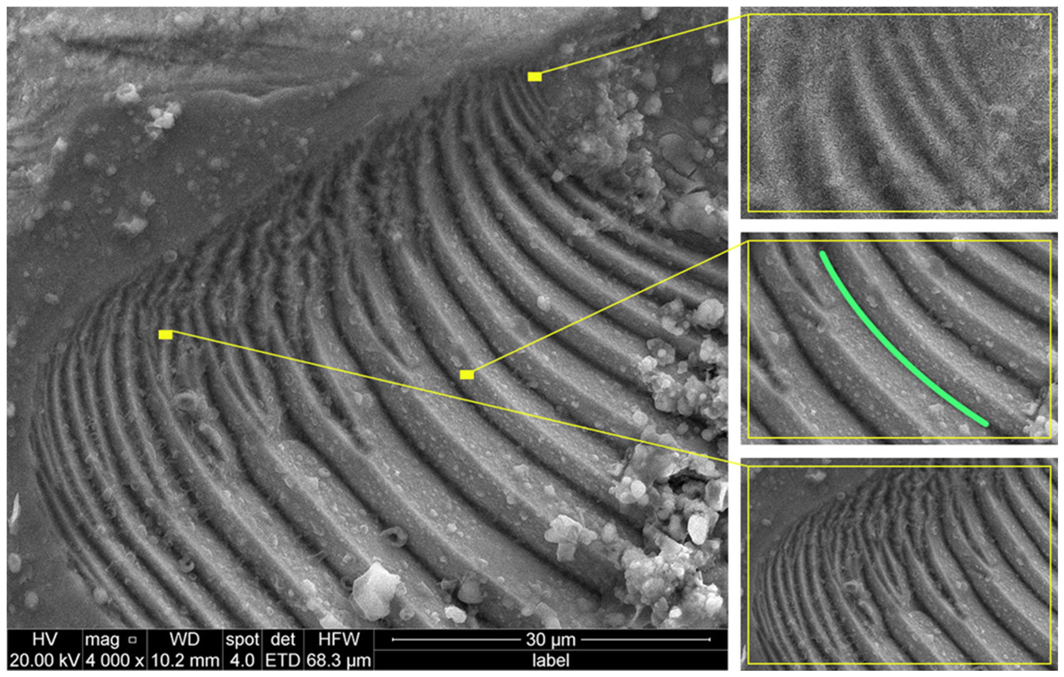
4.4. Mechanism 4: Screw Dislocation-Driven Spiral Growth and Step Formation
4.5. Concluding Discussion: The Complex Nature of Defect Formation and Self-Organization in Highly Doped InP Crystals
5. Limitations and Future Research
6. Conclusions
Author Contributions
Funding
Institutional Review Board Statement
Informed Consent Statement
Data Availability Statement
Conflicts of Interest
References
- Lin, Y.; Torsi, R.; Geohegan, D.B.; Robinson, J.A.; Xiao, K. Controllable Thin-Film Approaches for Doping and Alloying Transition Metal Dichalcogenides Monolayers. Adv. Sci. 2021, 8, 2004249. [Google Scholar] [CrossRef]
- Suchikova, Y.A.; Kidalov, V.V.; Sukach, G.A. Influence of the Carrier Concentration of Indium Phosphide on the Porous Layer Formation. J. Nano-Electron. Phys. 2010, 2, 75–81. [Google Scholar]
- Pastuszak, J.; Węgierek, P. Photovoltaic Cell Generations and Current Research Directions for Their Development. Materials 2022, 15, 5542. [Google Scholar] [CrossRef]
- Euvrard, J.; Yan, Y.; Mitzi, D.B. Electrical Doping in Halide Perovskites. Nat. Rev. Mater. 2021, 6, 531–549. [Google Scholar] [CrossRef]
- Arnold, A.J.; Schulman, D.S.; Das, S. Thickness Trends of Electron and Hole Conduction and Contact Carrier Injection in Surface Charge Transfer Doped 2D Field Effect Transistors. ACS Nano 2020, 14, 13557–13568. [Google Scholar] [CrossRef] [PubMed]
- Priyadarshini, P.; Das, S.; Naik, R. A Review on Metal-Doped Chalcogenide Films and Their Effect on Various Optoelectronic Properties for Different Applications. RSC Adv. 2022, 12, 9599–9620. [Google Scholar] [CrossRef] [PubMed]
- Badi, N.; Theodore, A.M.; Alghamdi, S.A.; Al-Aoh, H.A.; Lakhouit, A.; Roy, A.S.; Alatawi, A.S.; Ignatiev, A. Fabrication and Characterization of Flexible Solid Polymers Electrolytes for Supercapacitor Application. Polymers 2022, 14, 3837. [Google Scholar] [CrossRef]
- Suchikova, Y.; Kidalov, V.; Sukach, G. Blue Shift of Photoluminescence Spectrum of Porous InP. ECS Trans. 2019, 25, 59–64. [Google Scholar] [CrossRef]
- Sychikova, Y.A.; Kidalov, V.V.; Sukach, G.A. Dependence of the Threshold Voltage in Indium-Phosphide Pore Formation on the Electrolyte Composition. J. Surf. Investig. X-ray Synchrotron Neutron Tech. 2013, 7, 626–630. [Google Scholar] [CrossRef]
- Zhao, H.; Pinna, S.; Sang, F.; Song, B.; Brunelli, S.T.Š.; Coldren, L.A.; Klamkin, J. High-Power Indium Phosphide Photonic Integrated Circuits. IEEE J. Sel. Top. Quantum Electron. 2019, 25, 4500410. [Google Scholar] [CrossRef]
- Fridlander, J.; Sang, F.; Rosborough, V.; Gambini, F.; Šuran-Brunelli, S.T.; Chen, J.R.; Numata, K.; Stephen, M.; Coldren, L.A.; Klamkin, J. Dual Laser Indium Phosphide Photonic Integrated Circuit for Integrated Path Differential Absorption Lidar. IEEE J. Sel. Top. Quantum Electron. 2022, 28, 6100208. [Google Scholar] [CrossRef]
- Mukherjee, C.; Deng, M.; Nodjiadjim, V.; Riet, M.; Mismer, C.; Guendouz, D.; Caillaud, C.; Bertin, H.; Vaissiere, N.; Luisier, M.; et al. Towards Monolithic Indium Phosphide (InP)-Based Electronic Photonic Technologies for Beyond 5G Communication Systems. Appl. Sci. 2021, 11, 2393. [Google Scholar] [CrossRef]
- Suchikova, Y.; Bohdanov, I.; Kovachov, S.; Dannik, L.; Moskina, A.M.; Popov, A.I. Texturing of Indium Phosphide for Improving the Characteristics of Space Solar Cells. In Proceedings of the 2021 IEEE 12th International Conference on Electronic Information Technologies (ELIT), Lviv, Ukraine, 19–21 May 2021. [Google Scholar] [CrossRef]
- Suchikova, Y.; Kovachov, S.; Karipbaev, Z.; Zhydachevskyy, Y.; Lysak, A.; Popov, A.I. Influence of Electrolyte Composition on Indium Phosphide Pore Geometry and Applications in Solar Energy. In Proceedings of the 2023 IEEE 4th KhPI Week of Advanced Technology (KhPIWeek), Kharkiv, Ukraine, 2–6 October 2023. [Google Scholar] [CrossRef]
- Bhuiyan, A.G.; Hashimoto, A.; Yamamoto, A. Indium Nitride (InN): A Review on Growth, Characterization, and Properties. J. Appl. Phys. 2003, 94, 2779–2808. [Google Scholar] [CrossRef]
- Suchikova, J.A. Synthesis of Indium Nitride Epitaxial Layers on a Substrate of Porous Indium Phosphide. J. Nano-Electron. Phys. 2015, 7, 03017. [Google Scholar]
- Mikhrin, S.B.; Shtel’makh, K.F. Partly Filled Impurity Band Formation in Compensated InP. Phys. B Condens. Matter 2001, 308–310, 881–883. [Google Scholar] [CrossRef]
- Wang, Z.; Fan, C.; Shen, Z.; Hua, C.; Hu, Q.; Sheng, F.; Lu, Y.; Fang, H.; Qiu, Z.; Lu, J.; et al. Defects Controlled Hole Doping and Multivalley Transport in SnSe Single Crystals. Nat. Commun. 2018, 9, 47. [Google Scholar] [CrossRef]
- Usseinov, A.; Koishybayeva, Z.; Platonenko, A.; Akilbekov, A.; Purans, J.; Pankratov, V.; Suchikova, Y.; Popov, A.I. Ab-Initio Calculations of Oxygen Vacancy in Ga2O3 Crystals. Latv. J. Phys. Tech. Sci. 2021, 58, 3–10. [Google Scholar] [CrossRef]
- Arbia, M.B.; Smiri, B.; Demir, I.; Saidi, F.; Altuntas, I.; Hassen, F.; Maaref, H. Theoretical Analyses of the Carrier Localization Effect on the Photoluminescence of In-Rich InGaAs Layer Grown on InP. Mater. Sci. Semicond. Process. 2022, 140, 106411. [Google Scholar] [CrossRef]
- Kallstenius, T.; Backstrom, J.; Smith, U.; Stoltz, B. On the Degradation of InGaAsP/InP-Based Bulk Lasers. J. Light. Technol. 1999, 17, 2584–2594. [Google Scholar] [CrossRef]
- Weyher, J.L.; Kelly, J.J. Defect-Selective Etching of Semiconductors. In Springer Handbook of Crystal Growth; Dhanaraj, G., Byrappa, K., Prasad, V., Dudley, M., Eds.; Springer Handbooks: Berlin/Heidelberg, Germany, 2010. [Google Scholar] [CrossRef]
- Weyher, J.L. Defect Sensitive Etching of Nitrides: Appraisal of Methods. Cryst. Res. Technol. 2011, 47, 333–340. [Google Scholar] [CrossRef]
- Kulkarni, M.S. A Review and Unifying Analysis of Defect Decoration and Surface Polishing by Chemical Etching in Silicon Processing. Ind. Eng. Chem. Res. 2003, 42, 2558–2588. [Google Scholar] [CrossRef]
- Zhuang, D.; Edgar, J.H. Wet Etching of GaN, AlN, and SiC: A Review. Mater. Sci. Eng. R Rep. 2005, 48, 1–46. [Google Scholar] [CrossRef]
- Murgai, A.; Gatos, H.C.; Witt, A.F. Quantitative Analysis of Microsegregation in Silicon Grown by the Czochralski Method. J. Electrochem. Soc. 1976, 123, 224–229. [Google Scholar] [CrossRef]
- Tavakoli, M.H.; Wilke, H. Numerical Investigation of Heat Transport and Fluid Flow during the Seeding Process of Oxide Czochralski Crystal Growth Part 2: Rotating Seed. Cryst. Res. Technol. 2007, 42, 688–698. [Google Scholar] [CrossRef]
- Suchikova, Y.A.; Kidalov, V.V.; Sukach, G.A. Influence of Dislocations on the Process of Pore Formation in n-InP (111) Single Crystals. Semiconductors 2011, 45, 121–124. [Google Scholar] [CrossRef]
- Bader, K.; Gille, P. Single Crystal Growth of FeGa3 and FeGa3−x Gex from High-Temperature Solution Using the Czochralski Method. Cryst. Res. Technol. 2019, 55, 1900067. [Google Scholar] [CrossRef]
- Lu, C.-W.; Chen, J.-C. Numerical Simulation of Thermal and Mass Transport during Czochralski Crystal Growth of Sapphire. Cryst. Res. Technol. 2010, 45, 371–379. [Google Scholar] [CrossRef]
- Abrosimov, N.V.; Rossolenko, S.N.; Thieme, W.; Gerhardt, A.; Schröder, W. Czochralski Growth of Si- and Ge-Rich SiGe Single Crystals. J. Cryst. Growth 1997, 174, 182–186. [Google Scholar] [CrossRef]
- Trukhanov, E.M.; Fritzler, K.B.; Vasilenko, A.P.; Kolesnikov, A.V.; Kasimkin, P.V.; Moskovskih, V.A. Dislocation Structure of Ge Crystals Grown by Low Thermal Gradient Czochralski Technique. J. Cryst. Growth 2017, 468, 457–461. [Google Scholar] [CrossRef]
- Subramanyam, N.; Tsai, C.T. Dislocation Reduction in GaAs Crystal Grown from the Czochralski Process. J. Mater. Process. Technol. 1995, 55, 278–287. [Google Scholar] [CrossRef]
- Pendurti, S.; Prasad, V.; Zhang, H. Modelling Dislocation Generation in High Pressure Czochralski Growth of InP Single Crystals: Part I. Construction of a Visco-Plastic Deformation Model. Modell. Simul. Mater. Sci. Eng. 2005, 13, 249–266. [Google Scholar] [CrossRef]
- Giannattasio, A.; Senkader, S.; Falster, R.J.; Wilshaw, P.R. Generation of Dislocation Glide Loops in Czochralski Silicon. J. Phys. Condens. Matter 2002, 14, 12981–12987. [Google Scholar] [CrossRef]
- Inoue, T.; Komatsu, H. Effects of the Crystal Diameter on the Dislocation Density in KCl Crystals Grown by the Czochralski Method. Krist. Und Tech. 1979, 14, 1511–1519. [Google Scholar] [CrossRef]
- Gradwohl, K.-P.; Juda, U.; Sumathi, R.R. The Impact of the Dislocation Distribution and Dislocation Type on the Charge Carrier Lifetime in Czochralski Germanium Single Crystals. J. Cryst. Growth 2021, 573, 126285. [Google Scholar] [CrossRef]
- Suchikova, Y.; Kovachov, S.; Lazarenko, A.; Bohdanov, I.; Popov, A.I. Nanopore Formation at the Junctions of the Polycrystal Intergranular Boundary Under Plastic Deformation. Latv. J. Phys. Tech. Sci. 2023, 60, 3–18. [Google Scholar] [CrossRef]
- Kovachov, S.; Bohdanov, I.; Bardus, I.; Drozhcha, D.; Tikhovod, K.; Khrekin, A.; Bondarenko, V.; Kosogov, I.; Suchikova, Y. About Synthesis Mechanism of Periodic Oxide Nanocrystallites on Surface of Single-Crystal InP. Phys. Chem. Solid State 2023, 24, 159–165. [Google Scholar] [CrossRef]
- Dyer, L.D. Dislocation-Free Czochralski Growth of ⟨110⟩ Silicon Crystals. J. Cryst. Growth 1979, 47, 533–540. [Google Scholar] [CrossRef]
- Sanjarovskii, N.A.; Parfenteva, I.B.; Yugova, T.G.; Knyazev, S.N. Defect Structure of Tin-Doped InAs Single Crystals Grown by the Czochralski Method. Crystallogr. Rep. 2022, 67, 1095–1098. [Google Scholar] [CrossRef]
- Huang, Z.; Wu, S.; Chen, B.; Tang, S.; Ma, Y.; Liu, W. Tailoring the Defects and Resistivity in CdZnTe Single Crystal via One-Step Annealing with CdTe Compound. Vacuum 2023, 217, 112519. [Google Scholar] [CrossRef]
- Michałowski, P.P.; Złotnik, S.; Rudziński, M. Three Dimensional Localization of Unintentional Oxygen Impurities in Gallium Nitride. Chem. Commun. 2019, 55, 11539–11542. [Google Scholar] [CrossRef]
- Yu, B.; Xu, L.; Wang, S.; Huang, P.; Liu, H.; Zhang, L.; Li, X.; Wang, B.; Yu, G.; Sui, T. Study on Burgers Vector of Dislocations in KDP (010) Faces and Screw Dislocation Growth Mechanism of (101) Faces. RSC Adv. 2021, 11, 7897–7902. [Google Scholar] [CrossRef] [PubMed]
- Suchikova, Y.O.; Bogdanov, I.T.; Kovachov, S.S. Oxide Crystals on the Surface of Porous Indium Phosphide. Arch. Mater. Sci. Eng. 2019, 98, 49–56. [Google Scholar] [CrossRef]
- Bohdanov, I.; Bardus, Y.; Kovachov, S.; Tsybuliak, N.; Lopatina, H.; Suchikova, Y. Periodic Nanostructures by “Parquet Floor” Type on InP Surface. In Proceedings of the 2022 IEEE 2nd Ukrainian Microwave Week (UkrMW), Kharkiv, Ukraine, 14–18 November 2022. [Google Scholar] [CrossRef]
- Carlson, D.J.; Bliss, D.F. Near Infrared Microscopy for the Determination of Dopant Distributions and Segregation in n-Type/InP. In Proceedings of the LEOS 1992 Summer Topical Meeting Digest on Broadband Analog and Digital Optoelectronics, Optical Multiple Access Networks, Integrated Optoelectronics, and Smart Pixels, Newport, RI, USA, 21–24 April 1992. [Google Scholar] [CrossRef]
- Fornari, R.; Taddia, M.; Ranno, D. Cadmium Segregation in LEC-Grown InP. Mater. Lett. 1991, 10, 404–406. [Google Scholar] [CrossRef]
- Seidl, A.; Mosel, F.; Müller, G. Non-Uniformity of Fe Doping in Semi-Insulating LEC-Grown InP and Its Characterization by Various Mapping Methods. Mater. Sci. Eng. B 1994, 28, 107–110. [Google Scholar] [CrossRef]
- Yanlei, S.; Niefeng, S.; Chengyan, X.; Shujie, W.; Peng, L.; Chunlei, M.; Senfeng, X.; Wei, W.; Chunmei, C.; Lijie, F.; et al. Thermal Field of 6-Inch Indium Phosphide Single Crystal Grown by Semi-Sealed Czochralski Method. J. Inorg. Mater. 2023, 38, 335–342. [Google Scholar] [CrossRef]
- Takagi, K.; Fukazawa, T.; Ishii, M. Inversion of the Direction of the Solid-Liquid Interface on the Czochralski Growth of GGG Crystals. J. Cryst. Growth 1976, 32, 89–94. [Google Scholar] [CrossRef]
- Wang, S.; Sun, N.; Fu, L.; Wang, Y.; Li, Z.; Chen, C.; Shao, H.; Shi, Y.; Li, X.; Lin, J.; et al. Thermodynamics and Kinetics of In Situ Synthesized In-P Melt by the Phosphorus Injection and Its Solidification Behavior. J. Alloys Compd. 2022, 903, 163900. [Google Scholar] [CrossRef]
- Wang, P.; Li, X.; Wang, B.; Zhang, J.; Sun, T.; Zhang, Y.; Huang, X.; Zhu, J.; Chen, H.; Wang, S. Regulation of the Temperature Field and Evolution of the Melt Convection Field During InP Crystal Growth with the Vertical Gradient Freeze Method. J. Electron. Mater. 2023, 52, 7346–7364. [Google Scholar] [CrossRef]
- Morton, J.L.; Ma, N.; Bliss, D.F.; Bryant, G.G. Dopant Segregation During Liquid-Encapsulated Czochralski Crystal Growth in a Steady Axial Magnetic Field. J. Cryst. Growth 2002, 242, 471–485. [Google Scholar] [CrossRef]
- Feigelson, R.S. Crystal Growth History: Theory and Melt Growth Processes. J. Cryst. Growth 2022, 594, 126800. [Google Scholar] [CrossRef]
- Frank, F.C. The Influence of Dislocations on Crystal Growth. Discuss. Faraday Soc. 1949, 5, 48. [Google Scholar] [CrossRef]
- Tada, K.; Tatsumi, M.; Morioka, M.; Araki, T.; Kawase, T. InP Substrates: Production and Quality Control. In Semiconductors and Semimetals; Elsevier: Amsterdam, The Netherlands, 1990; pp. 175–241. [Google Scholar] [CrossRef]
- Cederberg, J.G.; Overberg, M.E. InP Substrate Evaluation by MOVPE Growth of Lattice Matched Epitaxial Layers. J. Cryst. Growth 2011, 315, 48–52. [Google Scholar] [CrossRef]
- Klapper, H. Generation and Propagation of Defects During Crystal Growth. In Springer Handbook of Crystal Growth; Springer: Berlin/Heidelberg, Germany, 2010; pp. 333–346. [Google Scholar] [CrossRef]
- Cottrell, A.H. Theory of Dislocations. Prog. Met. Phys. 1953, 4, 205–264. [Google Scholar] [CrossRef]
- Klapper, H.; Rudolph, P. Defect Generation and Interaction during Crystal Growth. In Handbook of Crystal Growth; Elsevier: Amsterdam, The Netherlands, 2015; pp. 1093–1141. [Google Scholar] [CrossRef]
- Böer, K.W.; Pohl, U.W. Crystal Defects. In Semiconductor Physics; Springer: Cham, Switzerland, 2023. [Google Scholar] [CrossRef]
- Suchikova, Y.; Lazarenko, A.; Kovachov, S.; Usseinov, A.; Karipbaev, Z.; Popov, A.I. Formation of porous Ga2O3/GaAs layers for electronic devices. In Proceedings of the 2022 IEEE 16th International Conference on Advanced Trends in Radioelectronics, Telecommunications and Computer Engineering (TCSET), Lviv-Slavske, Ukraine, 22–26 February 2022; pp. 1–4. [Google Scholar]
- Usseinov, A.B.; Karipbayev, Z.T.; Purans, J.; Kakimov, A.B.; Bakytkyzy, A.; Zhunusbekov, A.M.; Koketai, T.A.; Kozlovskyi, A.L.; Suchikova, Y.; Popov, A.I. Study of β-Ga2O3 Ceramics Synthesized under Powerful Electron Beam. Materials 2023, 16, 6997. [Google Scholar] [CrossRef]
- Sills, R.B.; Cai, W. Free Energy Change of a Dislocation Due to a Cottrell Atmosphere. Philos. Mag. 2018, 98, 1491–1510. [Google Scholar] [CrossRef]
- Katzarov, I.H.; Drenchev, L.B.; Pashov, D.L.; Zarrouk, T.N.A.T.; Al-lahham, O.; Paxton, A.T. Dynamic Strain Aging and the Role of the Cottrell Atmosphere. Phys. Rev. Mater. 2022, 6, 063603. [Google Scholar] [CrossRef]
- Nowak, C.; Spataru, C.D.; Chu, K.; Zhou, X.W.; Sills, R.B. Molecular Dynamics Study of Hydrogen Cottrell Atmosphere in Aluminum: Influence of Solute-Solute Interactions in the Dislocation Core. Phys. Rev. Mater. 2024, 8, 055404. [Google Scholar] [CrossRef]
- Cottrell, A.H.; Bilby, B.A. A Mechanism for the Growth of Deformation Twins in Crystals. Philos. Mag. 1951, 42, 573–581. [Google Scholar] [CrossRef]
- Cottrell, A.H.; Bilby, B.A. Dislocation Theory of Yielding and Strain Ageing of Iron. Proc. Phys. Soc. Sect. A 1949, 62, 49–62. [Google Scholar] [CrossRef]
- Oyama, Y.; Nishizawa, J.-I.; Kimura, T.; Tanno, T. Dislocation-Induced Deep Electronic States in InP: Photocapacitance Measurements. Phys. Rev. B 2006, 74, 235210. [Google Scholar] [CrossRef]
- Dorp, D.V.; Mannarino, M.; Arnauts, S.; Bender, H.; Merckling, C.; Moussa, A.; Vandervorst, W.; Schulze, A. Epitaxial Defects in Nanoscale InP Fin Structures Revealed by Wet-Chemical Etching. Crystals 2017, 7, 98. [Google Scholar] [CrossRef]
- Jordan, A.S.; Von Neida, A.R.; Caruso, R. The Theoretical and Experimental Fundamentals of Decreasing Dislocations in Melt Grown GaAs and InP. J. Cryst. Growth 1986, 79, 243–262. [Google Scholar] [CrossRef]
- Tatsumi, M.; Kawase, T.; Araki, T.; Yamabayashi, N.; Iwasaki, T.; Miura, Y.; Murai, S.; Tada, K.; Akai, S. Growth of Low-Dislocation-Density InP Single Crystals by the VCZ Method. In Proceedings of the 1st Intl Conf on Indium Phosphide and Related Materials for Advanced Electronic and Optical Devices, Norman, OK, USA, 28 November 1989; SPIE: Bellingham, WA, USA, 1989; Volume 1144. [Google Scholar] [CrossRef]
- Clark, J.; Ihli, J.; Schenk, A.; Kim, Y.-Y.; Kulak, A.N.; Holden, M.A.; Walsh, C.L.; Jacques, S.D.; Ashbrook, S.E.; Meldrum, F.C.; et al. Three-Dimensional Imaging of Dislocation Propagation during Crystal Growth and Dissolution. Nat. Mater. 2015, 14, 780–784. [Google Scholar] [CrossRef]
- Kuhlmann-Wilsdorf, D. The Theory of Dislocation-Based Crystal Plasticity. Philos. Mag. A 1999, 79, 955–1008. [Google Scholar] [CrossRef]
- Weyher, J.L.; Kelly, J.J. Defect Selective Photoetching of GaN: Progress, Applications and Prospects. Prog. Cryst. Growth Charact. Mater. 2024, 70, 100623. [Google Scholar] [CrossRef]
- Faktor, M.M.; Stevenson, J.L. The Detection of Structural Defects in GaAs by Electrochemical Etching. J. Electrochem. Soc. 1978, 125, 621–629. [Google Scholar] [CrossRef]
- Seidel, H.; Csepregi, L.; Heuberger, A.; Baumgärtel, H. Anisotropic Etching of Crystalline Silicon in Alkaline Solutions: I. Orientation Dependence and Behavior of Passivation Layers. J. Electrochem. Soc. 1990, 137, 3612–3626. [Google Scholar] [CrossRef]
- Bland, L.G.; Gusieva, K.; Scully, J.R. Effect of Crystallographic Orientation on the Corrosion of Magnesium: Comparison of Film Forming and Bare Crystal Facets Using Electrochemical Impedance and Raman Spectroscopy. Electrochim. Acta 2017, 227, 136–151. [Google Scholar] [CrossRef]
- Speidel, A.; Su, R.; Mitchell-Smith, J.; Dryburgh, P.; Bisterov, I.; Pieris, D.; Li, W.; Patel, R.; Clark, M.; Clare, A.T. Crystallographic Texture Can Be Rapidly Determined by Electrochemical Surface Analytics. Acta Mater. 2018, 159, 89–101. [Google Scholar] [CrossRef]
- Bailey, S.G.; Landis, G.A.; Wilt, D.M. Effect of Crystal Orientation on Anisotropic Etching and MOCVD Growth of Grooves on GaAs. J. Electrochem. Soc. 1989, 136, 3444–3449. [Google Scholar] [CrossRef]
- Tiginyanu, I.M.; Langa, S.; Christophersen, M.; Carstensen, J.; Sergentu, V.; Foca, E.; Rios, O.; Föll, H. Properties of 2D and 3D Dielectric Structures Fabricated by Electrochemical Dissolution of III-V Compounds. MRS Proc. 2001, 692, 7. [Google Scholar] [CrossRef]
- Jönsson, A.; Xu, P.; Reitemeier, J.; Bohn, P.W.; Fay, P. Wet Etch Methods to Achieve Submicron Active Area Self-Aligned Vertical Sb-Heterostructure Backward Diodes. Mater. Sci. Semicond. Process. 2024, 171, 108036. [Google Scholar] [CrossRef]
- Stirland, D.J.; Straughan, B.W. A Review of Etching and Defect Characterisation of Gallium Arsenide Substrate Material. Thin Solid Film. 1976, 31, 139–170. [Google Scholar] [CrossRef]
- Feigelson, R.S. Crystal Growth through the Ages. In Handbook of Crystal Growth; Elsevier: Amsterdam, The Netherlands, 2015; pp. 1–83. [Google Scholar] [CrossRef]
- Anttila, O. Czochralski Growth of Silicon Crystals. In Handbook of Silicon Based MEMS Materials and Technologies; Elsevier: Amsterdam, The Netherlands, 2015; pp. 18–55. [Google Scholar] [CrossRef]
- Cong, H.; Zhang, H.; Sun, S.; Yu, Y.; Yu, W.; Yu, H.; Zhang, J.; Wang, J.; Boughton, R.I. Morphological Study of Czochralski-Grown Lanthanide Orthovanadate Single Crystals and Implications on the Mechanism of Bulk Spiral Formation. J. Appl. Crystallogr. 2010, 43, 308–319. [Google Scholar] [CrossRef]
- Sumathi, R.R.; Abrosimov, N.; Gradwohl, K.-P.; Czupalla, M.; Fischer, J. Growth of Heavily-Doped Germanium Single Crystals for Mid-Infrared Applications. J. Cryst. Growth 2020, 535, 125490. [Google Scholar] [CrossRef]
- Liu, J.; Huang, Q.; Qian, Y.; Huang, Z.; Lai, F.; Lin, L.; Guo, M.; Zheng, W.; Qu, Y. Screw Dislocation-Driven Growth of the Layered Spiral-Type SnSe Nanoplates. Cryst. Growth Des. 2016, 16, 2052–2056. [Google Scholar] [CrossRef]
- Chu, Y.; Jing, S.; Liu, D.; Liu, J.; Zhao, Y. Morphological Control and Kinetics in Three Dimensions for Hierarchical Nanostructures Growth by Screw Dislocations. Acta Mater. 2019, 162, 284–291. [Google Scholar] [CrossRef]
- Hsu, C.C.; Xu, J.B.; Wilson, I.H. Spiral Growth of InP by Metalorganic Vapor Phase Epitaxy. Appl. Phys. Lett. 1994, 65, 1394–1396. [Google Scholar] [CrossRef]
- Luysberg, M.; Gerthsen, D. On the Dissociation of Dislocations in InP. Phys. Status Solidi A 1994, 146, 157–172. [Google Scholar] [CrossRef]
- Wang, F.; Wang, C.; Wang, Y.; Zhang, M.; Han, Z.; Yip, S.; Shen, L.; Han, N.; Pun, E.Y.; Ho, J.C. Diameter Dependence of Planar Defects in InP Nanowires. Sci. Rep. 2016, 6, 32910. [Google Scholar] [CrossRef]
- Shafi, A.M.; Das, S.; Khayrudinov, V.; Ding, E.-X.; Uddin, M.G.; Ahmed, F.; Sun, Z.; Lipsanen, H. Direct Epitaxial Growth of InP Nanowires on MoS2 with Strong Nonlinear Optical Response. Chem. Mater. 2022, 20, 9055–9061. [Google Scholar] [CrossRef]
- Wang, F.; Yip, S.; Dong, G.; Xiu, F.; Song, L.; Yang, Z.; Li, D.; Hung, T.F.; Han, N.; Ho, J.C. Manipulating III–V Nanowire Transistor Performance via Surface Decoration of Metal-Oxide Nanoparticles. Adv. Mater. Interfaces 2017, 4, 1700260. [Google Scholar] [CrossRef]
- Suchikova, Y.; Nazarovets, S.; Popov, A.I. Electrochemical Etching vs. Electrochemical Deposition: A Comparative Bibliometric Analysis. Electrochem 2025, 6, 18. [Google Scholar] [CrossRef]
- Sychikova, Y.; Kovachov, S.; Bohdanov, I.; Kosogov, I.; Drozhcha, D.; Karipbayev, Z.T.; Popov, A.I. Investigation of the Dynamics of Electrochemical Dissolution of n-InP (111) in Various Electrolyte Compositions and Determination of Optimal Etching Conditions. Nanosistemi Nanomater. Nanotehnologii 2024, 22, 1025. [Google Scholar] [CrossRef]
- Suchikova, Y.; Kovachov, S.; Karipbaev, Z.; Zhydachevskyy, Y.; Bohdanov, I.; Popov, A.I. Passivating Oxide Layers on the Surface of InP. In Proceedings of the 2024 IEEE 42nd International Conference on Electronics and Nanotechnology (ELNANO), Kyiv, Ukraine, 13–16 May 2024; pp. 223–226. [Google Scholar] [CrossRef]



| Item | Specifications | |
|---|---|---|
| Conductivity type | n-type | p-type |
| Dopant | S | Zn |
| Carrier concentration | 2.3 × 1018 cm−3 | |
| Orientation | (111), (100), (001) | |
| Crystal lattice | face-centered cubic (“zinc blende”) | |
| Mobility | (1.5–3.5) × 103 cm2/V·s | (50–70) × 103 cm2/V·s |
| Block | Parameter | Standard/Range |
|---|---|---|
| Cell | Material | PTFE, three-electrode configuration |
| WE/CE/RE | Working/counter/reference | InP/Pt mesh/Ag/AgCl (3 M KCl), with Luggin capillary |
| Area A | Exposed | Circular under O-ring (several mm2); measured optically |
| Electrolytes | Families | HF, HNO3, HCl in aqueous or aqueous–alcohol mixtures; prepared fresh |
| Temperature | Conditions | Room temperature (without thermostatting) |
| Modes | Control | Potentiostatic (typical); galvanostatic (control series) |
| Voltage/Current | Working regions | Several V vs. Ag/AgCl; J = 0.01–a few mA/cm2 (detailed for specific figures) |
| Monitoring | I(t) | Transient recording; stages: induction → activation → quasi-steady |
| Illumination | p-type | Continuous front illumination; without light, p-InP does not dissolve in the same conditions |
| SEM | Mode | JEOL-6490, SEI, ~10 kV, WD ~10 mm |
Disclaimer/Publisher’s Note: The statements, opinions and data contained in all publications are solely those of the individual author(s) and contributor(s) and not of MDPI and/or the editor(s). MDPI and/or the editor(s) disclaim responsibility for any injury to people or property resulting from any ideas, methods, instructions or products referred to in the content. |
© 2025 by the authors. Licensee MDPI, Basel, Switzerland. This article is an open access article distributed under the terms and conditions of the Creative Commons Attribution (CC BY) license (https://creativecommons.org/licenses/by/4.0/).
Share and Cite
Suchikova, Y.; Kovachov, S.; Bohdanov, I.; Popov, A.I.; Karipbayev, Z.T.; Kozlovskiy, A.L.; Konuhova, M. Investigation of Phase Segregation in Highly Doped InP by Selective Electrochemical Etching. Technologies 2025, 13, 395. https://doi.org/10.3390/technologies13090395
Suchikova Y, Kovachov S, Bohdanov I, Popov AI, Karipbayev ZT, Kozlovskiy AL, Konuhova M. Investigation of Phase Segregation in Highly Doped InP by Selective Electrochemical Etching. Technologies. 2025; 13(9):395. https://doi.org/10.3390/technologies13090395
Chicago/Turabian StyleSuchikova, Yana, Sergii Kovachov, Ihor Bohdanov, Anatoli I. Popov, Zhakyp T. Karipbayev, Artem L. Kozlovskiy, and Marina Konuhova. 2025. "Investigation of Phase Segregation in Highly Doped InP by Selective Electrochemical Etching" Technologies 13, no. 9: 395. https://doi.org/10.3390/technologies13090395
APA StyleSuchikova, Y., Kovachov, S., Bohdanov, I., Popov, A. I., Karipbayev, Z. T., Kozlovskiy, A. L., & Konuhova, M. (2025). Investigation of Phase Segregation in Highly Doped InP by Selective Electrochemical Etching. Technologies, 13(9), 395. https://doi.org/10.3390/technologies13090395


