Abstract
We demonstrate that selective electrochemical etching is a reliable method for detecting and observing the uneven concentration distribution of impurities in indium phosphide crystals, which accompanies the growth of highly doped crystals using the Czochralski method. Even though selective electrochemical etching, as a method of detecting defects in the crystal lattice, has been discussed many times in the literature, it has not yet been described for indium phosphide. In this work, we investigated etching in compositions of various selective electrolytes for InP of n- and p-type conductivity with different surface orientations. We present in detail the features of detecting the striped inhomogeneity of impurity distribution. The mechanisms and peculiarities of the formation of oxide crystallites on the surface of InP during electrochemical processing are presented, including structures like flower-like and parquet crystallites. The formation of porous surfaces, terraces, tracks, and crystallites is explained from the perspective of the defect-dislocation mechanism.
1. Introduction
The development of modern microelectronics requires researchers to create new materials with improved characteristics. At the same time, such materials must be characterized by the reliability and stability of their properties. Significant progress has been achieved using doping impurities in the growth of semiconductor crystals [1,2]. In particular, doping technologies have improved the characteristics of LEDs and solar cells [3,4]. Doping is crucial for tuning carrier injection properties at the metal/semiconductor interface [5].
An essential aspect of introducing doping impurities is the growth of crystals with controlled and regulated characteristics. The type of impurity and its content determine the type of conductivity, specific resistance, carrier concentration, mobility, etc. [6,7].
Among modern semiconductor materials, indium phosphide (InP) occupies a special place thanks to a range of unique properties [8,9]. Indium phosphide is used in photonic integrated circuits, laser technology, and photonics [10,11,12]. The radiation resistance of indium phosphide makes it a promising material for photovoltaics, particularly in space solar cells [13,14]. It has also been reported that InP is used as a substrate for growing epitaxial layers of nitrides [15,16].
The primary method for growing monocrystalline indium phosphide is the Czochralski process [17]. In this process, engineers face the challenge of controlling defects, as monocrystals with a high doping level tend to form many defects, including dislocation loops and clusters, point defects, and surface-related defects [18,19]. Moreover, dislocations serve as centers for powerful recombination carriers [20]. This can lead to severe degradation effects in devices [21]. Despite the extensive research on the impact of doping on the electrophysical and optical properties of semiconductors with various impurities, little work has been dedicated to the distribution of impurities in the volume of the crystal, i.e., the internal macromorphology of crystalline semiconductors.
Since direct observation of semiconductor defects is quite challenging, selective chemical or electrochemical etching is the most common and appropriate method for their observation [22,23]. Under certain conditions and with specific electrolytes, etch pits are observed on the crystal surface at the sites of defect concentration, which can be used to assess the nature and concentration (density) of semiconductor defects [24,25].
In this work, we summarize the results of many years of research on the morphology of indium phosphide and the influence of segregation phenomena on the processes of electrochemical dissolution of InP. Our choice is motivated by observing segregation phenomena through etch pits in semiconductors with different conductivity types and surface orientations. We demonstrate that Scanning Electron Spectroscopy (SEM) is an effective tool for studying the surface morphology of nanostructured semiconductor layers and can also be efficiently applied in assessing the distribution of impurities and defects within the crystal volume.
2. Materials and Methods
In this article, we summarize the results of more than fifteen years of research on indium phosphide (InP). Individual experimental series were carried out in different years and on samples from different batches; therefore, it would be inappropriate to reproduce complete technological maps for each historical case. Instead, we present a unified standardized methodology employed in the most recent series, which is applicable for reproducing the key results. Specific deviations (e.g., etchant composition or control mode) are indicated in the corresponding subsections of the results when discussing particular samples.
2.1. Materials
For the experiment, we used sets of single-crystalline indium phosphide of n- and p-type, doped to a carrier concentration of 2.3 × 1018 cm−3. The plates were cut from identical ingots with dimensions of 2 × 10 × 20 mm (Table 1).

Table 1.
Samples for the experiment.
Before the experiment, the plates were mechanically (with diamond paste) and chemically (with a polishing etchant) polished. After this, the plates were washed in distilled water and degreased in an alcohol solution. The method of electrochemical etching in solutions of selective etchants was chosen to study the correlations between segregation phenomena and changes in the morphological indicators of indium phosphide.
Aqueous and aqueous–alcohol hydrofluoric, nitric, and hydrochloric acid solutions were used as selective etchants. During the experiment, changes in the anodizing current were recorded. Fluctuations in the current determined the stages of electrochemical dissolution of the samples, and accordingly, the etching time was adjusted.
2.2. Electrochemical Cell and Electrodes
Electrochemical etching was performed in a three-electrode cell with a fluoroplastic (PTFE) body, equipped with an interchangeable mask. The investigated InP sample served as the working electrode, a platinum plate as the counter electrode, and an Ag/AgCl electrode (3 M KCl) as the reference electrode, connected through a Luggin capillary to minimize IR drop. All experiments were carried out at room temperature, without thermostatting, in a quiescent electrolyte. For some series, mild stirring with a magnetic stirrer in slow mode was used, which is explicitly noted where applicable in the description of experimental conditions.
2.3. Etching Solutions
For anodic etching, aqueous and aqueous–alcohol (ethanol) solutions of HF, HNO3, and HCl of analytical grade (Merck/Sigma-Aldrich, Darmstadt, Germany) were used. As a solvent, double-distilled or deionized water (18.2 MΩ·cm, Milli-Q) was employed. Working mixtures were prepared ex tempore immediately before each series of experiments, in polypropylene vessels to avoid contamination. Concentrations were chosen within working ranges that ensured stable anodic dissolution of InP without transition to electropolishing. For p-type samples, HF-containing mixtures were predominantly used, as they allowed reliable control of the dissolution rate, while for n-type samples, HNO3/HCl in aqueous and aqueous–alcohol media also proved effective. Optimization of the solution compositions was based on the prior literature and on our own preliminary experiments. The exact compositions for individual figures/samples are specified in the relevant subsections of the results.
2.4. Control Modes, Voltage/Current, and I(t) Recording
In the later series of anodic etching experiments, both potentiostatic and galvanostatic regimes were tested, with variation in initial conditions, holding times, and illumination intensity.
In the potentiostatic regime, the samples were initially kept at 0 V for 30–60 s, after which the potential was stepwise shifted into the working region (typically several volts relative to Ag/AgCl) with a subsequent holding period from tens to hundreds of seconds. In some cases, a slow linear voltage ramp (≈0.05–0.2 V/s) was applied to follow the characteristic transitions between passivation, active dissolution, and electropolishing.
In the galvanostatic regime, a constant current density from hundredths to units of mA/cm2 was maintained, while the voltage was recorded in time to capture the characteristic stages of the process. In all cases, anodic current transients I(t) were continuously monitored, typically comprising (i) an induction stage corresponding to the formation and restructuring of the oxide film, (ii) a current jump associated with breakdown and activation, and (iii) a quasi-steady dissolution stage. The etching duration was adjusted based on the shape of I(t).
For p-InP, continuous front illumination with white light (lamp or LED) was required in most electrolytes, since without illumination, dissolution did not occur under the same potentials. For n-InP, illumination was generally not necessary. The intensity and spectral characteristics of the light source are indicated for each experimental series separately.
2.5. Post-Treatment of Samples
Upon completion of electrochemical processing, the samples were immediately removed from the cell and thoroughly rinsed in several portions of deionized water to remove electrolyte residues. In cases where a thin organic or oxide film might remain on the surface, additional rinsing in alcohol (ethanol or isopropanol) was carried out to facilitate the removal of adsorbed components and to prevent the re-deposition of salts. Finally, the samples were dried with a stream of high-purity nitrogen to avoid water marks and dried electrolyte spots. To prevent subsequent structural or compositional changes (e.g., uncontrolled oxidation or the formation of artifact phases), the samples were stored under dry conditions at room temperature.
2.6. Electron Microscopy
Surface morphology after electrochemical treatment was examined using scanning electron microscopy (SEM) with a JEOL JSM-6490 instrument (JEOL Ltd., Tokyo, Japan) equipped with a secondary electron detector (SEI). Typical operating parameters included an accelerating voltage of 10 kV and a working distance (WD) of about 10 mm, which provided an optimal balance between spatial resolution and signal intensity. Images were acquired at different magnifications to assess both the overall appearance of etching figures and local microstructural details. To minimize beam-induced artifacts and surface charging, low probe currents and short exposures were used.
All experimental conditions are summarized in Table 2.
Table 2.
Generalized parameter set (default conditions).
3. Results
3.1. Investigation of Etch Pits on the Surface of InP with Different Crystallographic Orientations
Figure 1 demonstrates the surface morphology of indium phosphide samples of different crystallographic orientations during electrochemical etching in hydrochloric, hydrofluoric, and nitric acid solutions using a 25% solution by weight of each etchant. The samples were etched at a constant voltage of U = 3 V. It can be seen that in different acids, InP crystals are etched with the formation of a unique microrelief. However, general trends can be identified.
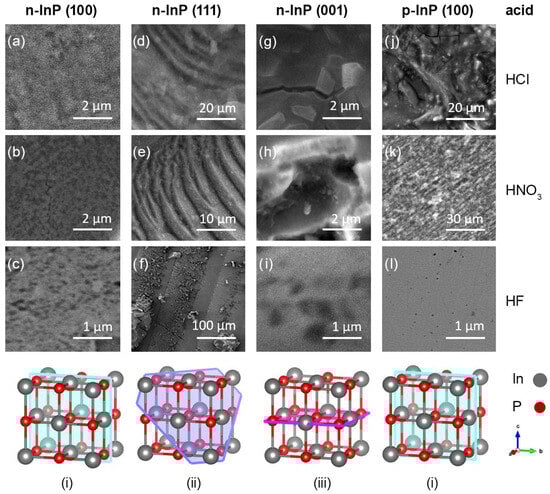
Figure 1.
Fragments of the surface morphology of indium phosphide after electrochemical treatment in different etchant compositions (a–l) and a schematic representation of the (100), (111), and (001) planes of the InP crystal lattice, respectively (i–iii).
Samples n-InP with a (100) surface orientation are etched with the formation of tiny pores evenly distributed over the surface (Figure 1a–c). Such pores are oriented along the current and grow deep into the crystal in thin, mutually parallel channels. Depending on the composition of the electrolyte, the diameter of such pores varies from 20 nm to 100 nm, and the porosity can reach 80%. The pores are cylindrical, oriented along the direction of the electric current, and extend deep into the crystal lattice, forming thin parallel channels. The porosity level can reach 80%, indicating a significant alteration in the crystal structure. The size and distribution of the pores change depending on the type of electrolyte used. In hydrochloric acid, the pores are more uniform and diminutive, whereas in hydrofluoric acid, they tend to be larger and more dispersed. A moderate pore size with a more rugged surface texture is observed in nitric acid.
N-InP samples with a (111) surface orientation demonstrate the formation of massive etch pits, tracks, and steps, indicating a more aggressive dissolution process (Figure 1d,e). Electrochemical treatment often results in the formation of oxide crystallites on the surface, especially noticeable in samples etched with hydrofluoric acid (Figure 1f). The most active electrochemical dissolution processes were manifested precisely during the etching of n-InP with a (111) surface orientation. The surfaces oriented towards (111) exhibit the most dynamic etching patterns with deep, irregular pits and pronounced crystalline features.
On the other hand, n-InP with a (001) orientation shows diverse morphological changes depending on the etching solution. In hydrochloric acid, cracks with embedded crystallites appear on the surface (Figure 1g). In hydrofluoric acid, extensive etching pits are formed (Figure 1h), while in nitric acid, relatively smaller pores are observed (Figure 1i).
InP samples of p-type conductivity demonstrate less susceptibility to electrochemical processing than n-type InP (Figure 1j,k). These samples show textured surfaces with either dispersed textures or isolated small etching pits. This suggests a more restrained etching process, likely due to the different electrical properties of p-type InP.
Overall, the study emphasizes the significant influence of crystallographic orientation on the etching behavior of InP. The (111) orientation is particularly prone to pronounced etching effects, making it suitable for studying surface and volume defects through selective electrochemical etching. These findings have implications for the fabrication of semiconductor devices, where control over surface morphology at the nanoscale can impact device performance.
3.2. Formation of Growth Defects in InP During Czochralski Method Growth
A layered heterogeneity in the distribution of defects is observed during the growth of indium phosphide using the Czochralski method [26]. As demonstrated in Figure 1e,f, this manifests as concentric rings during the etching of n-InP (111) in selective etchants. These rings result from the uneven distribution of impurities within the semiconductor volume during crystallization.
To understand the processes of uneven impurity distribution in grown single crystal ingots, let us briefly present the key points. The crucible has a melt-in contact with a seed crystal. The seed crystal is slowly released, allowing atoms from the melt to attach. An important aspect is that the seed crystal has a slightly lower temperature than the melt. As a result of this process, temperature gradients arise that affect the growth boundary.
Excessive concentrations of impurities in some crystal regions can lead to the formation of their complexes, which can be considered a new system component. Thus, uneven crystallization is observed during the growth of highly doped semiconductors using the Czochralski method, which is facilitated by new degrees of freedom. In other words, it can be asserted that phase transformations occurring at the boundary of areas with different impurity concentrations lead to the appearance of coherent and incoherent boundaries. Coherent boundaries do not disturb the structure and monocrystallinity of the semiconductor ingot. Incoherent boundaries, due to significant interphase differences, lead to the breaking of bonds and the formation of an intercrystalline border. This is manifested as the striation of the crystal structure.
Doping semiconductors with donor impurities to high concentrations leads to the appearance of microdefects and dislocations. Moreover, impurity atoms cause intrinsic point defects, among which are substitution atoms, interstitial atoms, vacancies, Frenkel pairs, and others. The presence of a high concentration of point defects, in turn, leads to twinning and dislocation clusters. This is manifested in segregation phenomena. In this sense, the impurity concentration can be considered a function of crystal growth.
Segregation lines exhibit periodicity and are striated. The cyclicality of the crystal growth rate can explain striation. The growth rate’s nonlinear character is due to dislocations in the crystal volume and the uneven distribution of the doping impurity.
Segregation lines appear as continuous lines perpendicular to the growth direction of the semiconductor grown from the melt (Figure 2). The accumulation of doping impurities, caused by fluctuations in the microscopic growth rate, occurs due to an imbalance in convection through temperature fluctuations at the seed/melt interface [27]. In Figure 2, one can observe etching figures on the surface of n-InP (111), which result from a selective etchant (HF solution) on areas of excess impurity content and impurity-depleted zones. Growth bands, which appear as areas with a high density of etch pits, are separated by unetched areas (Figure 2(1)).
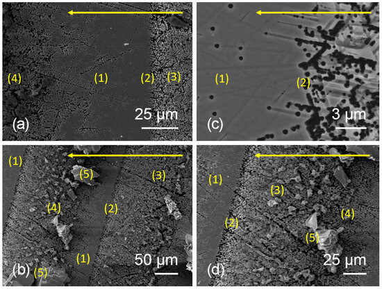
Figure 2.
Segregation lines of impurities observed after etching n-InP (111) in a 25% HF solution. Subfigures (a–d) correspond to different regions of the same sample, shown at varying magnifications, in order to demonstrate both large-scale and fine-scale features of segregation. The yellow arrows indicate the direction of crystal growth. Labels: (1) impurity-depleted areas; (2) the boundary between the segregation line and depleted areas; (3) zones of excessive impurity content; (4) transitional zone; (5) crystallites formed in the zone of excessive impurity content.
Segregation lines show an exciting feature. One edge has a clear boundary dividing the zones of excess and depleted impurity content (Figure 2(2)). Then, there is a gradual decrease in the number of etch pits (Figure 2(3)). Areas (4) in Figure 2 show the edge of the segregation band, which is “blurred.” In these areas, the concentration of pores (etch pits) is significantly lower due to the lower impurity concentration. Such observations indicate the direction of crystal growth. The width of the zone with increased impurity concentration is 100 nm, and the depleted zone is 120 µm. Our work investigates the concentration inhomogeneity of impurity distribution in more detail [28].
Consequently, we observe an increase in the concentration of inlet pores from the center to the periphery of the sample, which also gives an idea of the direction of crystal growth (in Figure 1, the direction of crystal growth is indicated by arrows). It should be noted that growth bands can affect the crystal lattice parameters within the zone of excessive impurity content but almost do not affect the change in lattice constants between bands [29,30]. Also, growth bands may appear due to the emergence of so-called “dislocation walls,” which manifest as irregular lines running perpendicular to the growth front. Dislocation walls arise due to the inhomogeneous accumulation of doping impurities along the growth front, transitioning from one layer to another as the crystal grows [31,32].
Such a sectoral distribution into zones of excessive impurity content and, conversely, impurity-depleted zones can, in turn, lead to the appearance of screw dislocations [33,34]. The semiconductor crystal around a screw dislocation represents a single atomic plane. Spiral steps move around the dislocation as excess impurity atoms are adsorbed on the surface. As a result, crystal growth is observed without the nucleation of new layers, i.e., the formation of a growth spiral (Figure 3). It can be seen that the height of the step is 5 µm. As a result of electrochemical etching, the steps delaminate into bands 1 µm wide. Their surface becomes loose and porous.

Figure 3.
Growth spirals of n-InP observed after etching in a selective electrolyte of 25% HNO3. The yellow boxes and lines mark enlarged regions of the same spiral structure shown at higher magnifications. The green line highlights the trajectory of a representative spiral step, illustrating its curvature and periodicity.
Generally, the screw dislocation plays a crucial role in crystal growth from the melt [35]. As mentioned earlier, such a dislocation represents a single atomic plane that grows around the dislocation axis due to the addition of atoms to an infinite source of kinks [36,37]. In turn, the step is anchored at the point of dislocation emergence [38]. The step’s inner parts rotate faster than the outer ones [39], causing the step to twist into a spiral.
During the cooling of the forming ingot from the melt, homogeneity of composition is determined by convective processes. Horizontal temperature and impurity concentration gradients cause significant axial and radial inhomogeneity. Moreover, the distribution of impurities in the crystal can be inhomogeneous not only along but also across the axis of crystal growth, as demonstrated in Figure 4. In this case, changes in the lattice parameter of the solid solution can cause elastic stresses [40,41].

Figure 4.
SEM image of cleavage in n-InP, demonstrating the formation of terraces after electrochemical processing of the crystal due to the etching of areas with increased impurity concentration. The yellow boxes indicate enlarged regions shown at higher magnifications. The green lines mark representative terrace steps, highlighting their curvature and periodicity.
Thus, temperature fluctuations in the crystallization zone significantly impact the formation of growth bands. These temperature fluctuations arise due to two mechanisms. Firstly, the crystal growth rate may vary across the crucible due to asymmetry in the temperature field. Secondly, convective processes can also cause temperature fluctuations.
3.3. Investigation of Etch Pits Along Dislocation Slip Lines
When etching the crystal in selective etchants, the formation of etch pits along slip lines and dissolution channels, which form close to the etch pits, can be observed (Figure 5). The diameter of the etch pits caused by this phenomenon is 100 nm. The length of the dissolution channel can reach up to 10 µm. In Figure 5c, the formation of tracks between pores with lengths ranging from 1 to 3 µm can be seen. The tracks’ cross-section thickness is between 100 and 200 nm. The aspect ratio ranges from 20 to 50.
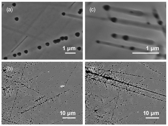
Figure 5.
Etch pits and dissolution channels along the line of an edge dislocation. Subfigure (a) shows isolated circular etch pits formed at dislocation sites; (b) demonstrates extended linear arrangements of etch pits across a wider field of view; (c) illustrates the development of dissolution channels that elongate from initial pits; (d) presents a dense dislocation line decorated with pits and channels, indicating a high local defect concentration.
Etch pits can form both on edge and screw dislocations. A dislocation is a source of elastic mechanical stresses, causing the formation of elastic deformations around it. Therefore, during the etching of InP in selective etchants, dislocations serve as the nucleation sites for forming primary (germinal) pores. Moreover, a dislocation can interact with point defects in the crystal volume, leading to an increased concentration of residual defects near the dislocation axis (the so-called “Cottrell atmosphere”) [42,43,44].
Across multiple n-InP(111) fields, the line-like etch features organize into two dominant in-plane families consistent with the ⟨110⟩ set on (111), producing obtuse intersections around 135°. This geometry is clearly visible in Figure 6, where crossing tracks preserve their directions after intersection. A third symmetry-equivalent family appears only weakly under our etching conditions, leading to a “two-family” field that nevertheless maintains the (111) crystallographic constraints. A quantitative orientation analysis (length-weighted rose diagrams, acute-angle distributions, and a Rayleigh test for axial data) rejects isotropy at high significance; complete statistics and raw angles are provided in the dataset (Zenodo, https://doi.org/10.5281/zenodo.16889714, accessed on 24 August 2025).

Figure 6.
SEM image of a porous surface of n-InP (111), showing the intersection of dissolution channels and tracks at an angle of 135°. The yellow circles (1–3) highlight representative regions where dissolution channels intersect. The yellow lines and angle markings indicate the measured orientation of crossing tracks, with the characteristic intersection angle of 135°.
3.4. Formation of Oxide Crystallites at Sites of Accumulation of Defects in the Crystal Lattice
Alternative electrochemical reactions can also accompany the process of electrochemical etching. These primarily include electrochemical polishing of the surface due to the etching of all surface irregularities. Furthermore, during etching, the surface can become covered with a continuous inseparable film, resulting from chemical interactions of the surface layers of indium phosphide with electrolyte ions. These films are typically oxide compounds of the first or second element of the semiconductor [45]. Such oxides can inhibit further dissolution of the crystal. In such a case, the etching process stops. Often, a continuous film, due to lattice mismatch with the substrate material (the semiconductor itself), can crack and split. This leads to the crystal’s re-etching at the film rupture sites. The formation of a porous space on the film itself can also occur. As a result of such behavior, the film becomes loose and is easily removed from the substrate.
The most important observation in this process is that the rupture of the film does not occur at spontaneous locations but specifically in areas of excessive impurity concentration. This is because such areas are supersaturated with dislocations. As a result, the formation of orderly “parquet” type oxide crystallites can be observed on the crystal surface (Figure 7).

Figure 7.
SEM image of oxide crystallites of the parquet type on the surface of n-InP (111), formed during electrochemical etching. The yellow boxes indicate magnified regions of the same sample, shown at higher resolution to illustrate details of the crystallite morphology. The yellow scale bars and arrows mark the characteristic dimensions of crystallites, including their length (up to 110 µm), width (≈3 µm), and height (≈7 µm).
The geometric dimensions of the crystallites are almost equal: length (100–130) µm; width and height about 7 µm. The distance between neighboring crystallites is 2 µm and between parquet blocks is 30–50 µm. The crystallites have a porous structure. It can be seen that the parquet blocks and crystallites easily align with each other. This indicates that the crystallites formed due to the spreading of the oxide film, due to the action of elastic stresses [46]. The longitudinal uniform shift of adjacent steps relative to each other occurs due to the slippage of dislocation loops. The shift stops after the partial emergence of the loop on the surface. Moreover, we often find surface outcrops of dislocation loops co-located with impurity-enriched regions (segregation lines).
Often on the surface of n-InP (111) during electrochemical processing, in areas of excessive impurity concentration, oxide crystallites of the flower type are formed (Figure 8a–c). The mechanism of this phenomenon is as follows. The rate of electrochemical deposition of reaction products on the surface (i.e., the growth of crystallites) depends on the arrival of atoms to the surface, as well as on the structure of the surface and processes occurring at the electrolyte/semiconductor interface.

Figure 8.
Flower-like crystallites on the surface of indium phosphide, formed in areas of excessive impurity concentration (a–c), and schematic representation of a crystallite (d) on flat (e) and porous (f) semiconductor surfaces at the semiconductor/electrolyte boundary. In panel (f), the numbers indicate atomic coordination at the porous surface: (1) surface atoms with one broken bond, (2) surface atoms with two broken bonds, and (3) surface atoms with three broken bonds. These sites act as preferential nucleation centers for crystallite growth.
Figure 8e presents a cross-section and boundary of the semiconductor/electrolyte with a flat (ideal) surface. Each surface atom of such a crystal has bonds with atoms in the volume. Thus, the surface energy is low, and the formation of new nucleation centers for crystallites is complicated due to the small number of broken bonds.
Dislocations that emerge on the crystal’s surface due to electrochemical etching are active centers of chemical reactions. Figure 8f shows that the surface atoms, due to the formation of pores, do not have all their “neighbors”; thus, the surface is characterized by many broken bonds. This means that atomically rough and imperfect surfaces have a higher rate of electrochemical deposition, i.e., a higher growth rate of oxide crystallites.
Also, the inhomogeneous distribution of impurities and their excessive concentration in segregation bands causes the appearance of a network of grain boundaries. Grain boundaries consist of individual dislocations or agglomerations of dislocations, forming so-called “dislocation walls.” Grain and subgrain boundaries are formed in ingots due to thermal stress during crystal growth. Grain boundaries act as charge capture centers, causing spatial inhomogeneity in charge transport, thereby impairing charge transfer. These walls and grain boundaries are nucleation centers for oxide crystallites on the crystal surface.
Thus, the study of defects in single crystals caused by impurity atoms is an essential factor in controlling the transport characteristics of electronic and photonic devices. The ability to manage defects by reducing or increasing their quantity could be the next step in creating modern functional materials. Eliminating impurity defects and concentration inhomogeneity in highly doped semiconductors is quite challenging. This necessitates further research to improve material quality by optimizing growth parameters and managing impurity defects. Efforts may be directed towards finding optimal conditions for thermal annealing of the semiconductor ingot, which can significantly reduce strained states in the semiconductor by creating new types of defects (stamping defects).
4. Discussion
In this chapter, we explore the mechanisms underlying defects’ formation and evolution in highly doped InP crystals, particularly during the Czochralski growth process and subsequent electrochemical etching. The behaviors observed in these crystals are multifaceted, governed by a complex interplay of factors that influence their structural and electronic properties. We compare our findings with established theories and models in crystal growth and materials science to better understand these phenomena. We draw parallels where empirical evidence from our study supports these frameworks.
The mechanisms discussed herein—including phase segregation, dislocation dynamics, and anisotropic etching—are not isolated events but interconnected processes that collectively shape the crystal’s morphology and behavior. While these theories offer valuable insights, they should not be viewed as mutually exclusive or singularly definitive explanations. Instead, they complement and reinforce each other, providing a more comprehensive picture of the self-organizing nature of defect formation in highly doped InP crystals. Empirical data presented in the previous chapter serve as the foundation for this discussion, offering direct or indirect confirmation of these mechanisms.
4.1. Mechanism 1: Phase Segregation During Czochralski Growth
Phase segregation in highly doped InP is governed by non-uniform dopant incorporation at the solid–liquid interface during Czochralski growth, where fluctuations in growth rate and thermal gradients give rise to segregation lines and growth bands [47,48,49,50,51]. Similar segregation behavior has been documented across semiconductor systems; for example, Abrosimov et al. reported SiGe crystals with banded impurity distributions originating from differences in distribution coefficients [31]. Numerical studies of seeding and melt transport further show that convective flows decisively shape dopant fields and, hence, segregation patterns [27], in line with observations for highly doped InP where melt dynamics control impurity profiles [52,53]. Magnetic-field-modified convection in liquid-encapsulated Czochralski growth likewise produces dopant non-uniformities, highlighting the sensitivity of segregation to melt hydrodynamics [54]. An additional pathway involves dislocation-assisted diffusion: in Ge grown under low thermal gradients, dislocation arrays were proposed as fast channels for impurity migration and local segregation [32], implying that dislocation control can mitigate banding [55,56].
Our data directly corroborate these literature trends. As shown above, selective electrochemical etching on InP(111) resolves mesoscopic segregation bands as families of line-like etch features that replicate the volumetric impurity morphology at the surface. The orientation selectivity (dominant ⟨110⟩ with secondary ⟨112⟩, six-peak rose patterns) and the characteristic intersection angles arise from the (111) crystallography and are consistent with segregation-guided anisotropic kinetics. The frequent co-localization of etch pits, terraces, and dissolution channels with these bands, together with the emergence of oxide crystallites, supports a segregation–dislocation coupling, wherein dislocations act both as sinks for impurities and as preferred sites for etch initiation—precisely the behavior anticipated by the dislocation-mediated segregation picture [32,55,56].
4.2. Mechanism 2: Dislocation Dynamics and Their Influence on Defect Formation
Dislocations—both screw and edge—act as elastic-strain centers that bias local impurity distribution and seed characteristic surface morphologies in highly doped InP [57,58]. Their role as traps and glide sources, widely documented in semiconductors [59,60,61,62,63,64], is consistent with our n-InP(111) observations: etch pits nucleate at defect sites and evolve into tracks, terraces, and dissolution channels that trace the underlying defect network. The Cottrell-atmosphere framework—impurity drift into dislocation stress fields [65,66,67,68,69]—provides a microscopic basis for these patterns and aligns with our evidence of compositionally modified surface within segregation bands and with the preferential initiation of oxide crystallites along those bands [19,42,64,66,70,71].
The anisotropy of the resulting morphologies follows naturally from crystallography and dislocation-induced stress. Modeling and experiments indicate that dislocation fields promote direction-selective attack in InP [34,72,73,74,75]. In our case, length-weighted orientation statistics reveal a characteristic multiplet of preferred in-plane directions on (111), with primary alignment along ⟨110⟩ and secondary components near ⟨112⟩, while the observed acute/obtuse intersections of track families are those expected for defect activity on {111} planes.
Finally, the literature shows that controlling dislocation density and distribution during growth mitigates defect-driven inhomogeneities [40,72,73]. This perspective dovetails with our finding that (111) plates, while most sensitive for revealing segregation, are also most responsive to the embedded dislocation network: moderating that network during growth should suppress band-linked nucleation and reduce anisotropic channeling during etching. In sum, our SEM results provide direct mesoscale confirmation that dislocation dynamics, together with their impurity atmospheres, govern the formation and orientation of dissolution features in highly doped InP, coherently linking established mechanisms [57,58,59,60,61,62,63,64,65,66,67,68,69,70,71,72,73,74,75] to the specific patterns measured in this work.
4.3. Mechanism 3: Electrochemical Etching and Anisotropic Surface Morphology
Electrochemical etching is a sensitive probe of defect structure in semiconductors, with morphology governed by crystallographic orientation and defect chemistry [76,77]. The orientation dependence observed in InP—where (111), (100), and (001) faces produce distinct etch figures—is consistent with established anisotropic etching behavior in related materials systems [78,79,80,81,82]. As reviewed by Weyher et al., defect-selective etching exploits differences in atomic bonding and surface stability across planes, yielding orientation-specific rates and morphologies that can be used to map defect distributions and internal structure [22,23]. Complementary work on wet etching in GaN, AlN, and SiC further underscores the role of crystallography and shows how anisotropy can be leveraged to delineate defective regions and improve surface quality [25]; conversely, chemical additives and parameter tuning can moderate anisotropy when desired [24].
Our results align directly with this framework. On InP(111), selective electrochemical etching reveals line-like families of tracks and terraces that trace segregation-linked defect networks. Length-weighted orientation statistics from SEM images yield a characteristic multiplet of preferred in-plane directions with dominant alignment along ⟨110⟩ and secondary components near ⟨112⟩; the intersection geometry of track families follows the symmetry expected for defect activity on {111} planes. These patterns are strongest on (111), which therefore serves as the most sensitive orientation for mesoscale visualization of segregation-driven defect organization in highly doped InP, while (100)/(001) present weaker or qualitatively different responses—again reflecting orientation-dependent surface energetics and kinetics.
In sum, anisotropic electrochemical etching provides a mesoscale, orientation-selective map of the defect landscape in InP that is fully consistent with the broader semiconductor literature [83,84]. The method both complements growth- and device-centric approaches and offers practical levers—via orientation choice and electrolyte design—for enhancing defect visibility or, when needed, moderating anisotropy to facilitate uniform processing.
4.4. Mechanism 4: Screw Dislocation-Driven Spiral Growth and Step Formation
Screw dislocations act as continuously operating step sources, producing spiral step patterns that govern surface evolution during growth and later during electrochemical attack [85,86,87,88,89,90]. This classical mechanism—well established for diverse crystals and exemplified by spiral step propagation from screw outcrops in KDP [44]—is directly consistent with our observations on highly doped InP: SEM images after selective electrochemical etching reveal anchored step bundles and spiral/terrace motifs that radiate from dislocation emergence sites and guide the formation of tracks and dissolution channels [91]. In our system, these step fields also organize near segregation lines, indicating that screw dislocations not only provide the kinematic source for step flow but also couple to impurity gradients, thereby imprinting mesoscale patterns that the etch amplifies.
The coupling of screw dislocations with impurity atmospheres and local stress fields explains the co-localization of oxide crystallites and the emergence of ordered (“parquet-like”) surface textures upon etching: dislocations act as sinks/sources for impurities under growth and processing conditions, biasing local chemistry and reactivity [40,92]. This picture aligns with reports that screw-dislocation stress fields induce directionally selective step propagation and dissolution, fixing preferred in-plane orientations and regularity of the spiral/terrace architecture [35].
Overall, our electrochemical-etch/SEM evidence shows that screw dislocations are the organizing centers that convert latent growth memory (step sources and impurity contrast) into the observed anisotropic relief—spirals, terraces, and channels—thus coherently linking the spiral-growth framework [85,86,87,88,89,90,91] with the InP morphologies uncovered in this work and with the stress/impurity-mediated ordering emphasized in prior studies [35,40,92].
4.5. Concluding Discussion: The Complex Nature of Defect Formation and Self-Organization in Highly Doped InP Crystals
The results presented here depict defect formation in highly doped InP as an intrinsically coupled, self-organizing process, where phase segregation during Czochralski growth, dislocation dynamics, and anisotropic surface kinetics act in concert. As shown above, segregation bands originating from melt transport and interfacial partitioning are modulated by dislocation networks, which concentrate impurities and imprint step/terrace fields on the crystal. During electrochemical processing, these latent contrasts are selectively amplified, yielding the patterned morphologies documented in our analysis.
Within this framework, electrochemical selective etching offers a distinctive methodological advantage for mesoscale, orientation-resolved visualization of segregation features on bulk-grown crystals. In contrast to bottom-up CVD nanowire approaches, where defect statistics are inferred indirectly from nanowire morphology or TEM analyses [93,94], or to device-level surface modulation via metal-oxide nanoparticle decoration [95], the electrochemical route provides a direct, spatially resolved map of segregation-linked defect organization over comparatively large areas, which is valuable both for mechanistic studies and quality control. At the same time, these techniques are complementary: growth-based and nanoscale probes supply the atomic-scale detail that our mesoscale mapping contextualizes.
A broader bibliometric perspective corroborates this complementarity: while electrochemical deposition has historically dominated applications in catalysis, energy storage, and biosensing, electrochemical etching has been central to defect visualization, porous architectures, and photonic functionalities [96,97,98]. Our findings therefore situate InP electrochemical etching squarely within this landscape, emphasizing its role in defect science and its synergy with state-of-the-art fabrication and characterization methods.
In sum, the defect patterns observed in highly doped InP arise from the interplay of growth dynamics, impurity partitioning, and dislocation-mediated fields, later expressed through anisotropic dissolution. Recognizing and exploiting this coupling—via crystallographic orientation, electrolyte design, and integration with complementary growth/characterization methods—provides a clear pathway to control and mitigate defect organization in InP and related semiconductor systems.
In conclusion, this study reaffirms the complex nature of crystal growth in highly doped InP and the importance of considering the myriad factors contributing to defect formation. The self-organizing behavior observed in these crystals highlights the sophistication of the processes at play and calls for further research to unravel the intricate mechanisms that drive the formation of defects and influence the material properties of semiconductors.
5. Limitations and Future Research
This study has an integrative character and focuses primarily on correlating the morphological features revealed by selective electrochemical etching with the defect structure of highly doped InP verified by SEM. The experimental framework was limited to representative etching regimes, specific dopants (S for n-type, Zn for p-type) at a high carrier concentration, and three crystallographic orientations. Complementary diffraction techniques such as SAED in HR-TEM were not performed. These restrictions, together with the potential influence of oxide formation and etching anisotropy, highlight the need for further cross-validation with independent methods.
Future investigations should expand the parameter space of etching regimes and doping types, apply advanced structural probes (HR-TEM/SAED, HRXRD, EBSD), and systematically benchmark the sensitivity of electrochemical etching against alternative defect characterization techniques such as SIMS, Raman, or EBIC. Particular attention should be paid to the quantitative calibration of etching features with dislocation density and impurity distribution. Addressing these directions would transform electrochemical etching from a predominantly qualitative descriptor into a standardized, quantitatively validated methodology for quality control of InP crystals.
6. Conclusions
Observing growth steps and segregation lines in highly doped InP crystals is a challenging task that requires a combination of complementary techniques. Our study demonstrates that electrochemical selective etching, when combined with scanning electron microscopy, provides an effective means to detect structural segregation phenomena at the submicron scale.
The results show that p-type InP crystals exhibit only weakly pronounced or difficult-to-detect impurity inhomogeneities, whereas (111)-oriented plates prove to be the most suitable for revealing segregation bands through the appearance of etch pits at defect accumulation sites. The uneven distribution of dopants, arising from non-stationary growth conditions, significantly affects the structural and electronic properties of the semiconductor. Moreover, edge and screw dislocations strongly influence the observed morphology, giving rise to growth spirals, dissolution channels, and terraces.
Electrochemical treatment also induces the formation of oxide crystallites, including flower-like and parquet-type structures, particularly in regions of excessive impurity concentration along segregation lines. These phenomena highlight the role of dislocations and local impurity gradients in driving surface modification during etching.
Overall, the study confirms that the concentration distribution of impurities reflects the interplay of growth parameters and structural defects, offering a valuable tool for investigating segregation phenomena and for controlling the quality of InP single crystals used in semiconductor applications.
Author Contributions
Conceptualization, Y.S. and A.I.P.; methodology, Y.S.; software, S.K. and M.K.; validation, Y.S., S.K. and A.I.P.; formal analysis, Y.S. and M.K.; investigation, S.K., I.B., Z.T.K., A.L.K., M.K. and Y.S.; resources, S.K., I.B., Z.T.K. and A.L.K.; data curation Y.S. and S.K.; writing—original draft preparation, Y.S. and A.I.P.; writing—review and editing, Y.S., M.K. and A.I.P.; visualization, S.K.; supervision, A.I.P.; project administration, Y.S. and A.I.P.; funding acquisition, A.I.P., Y.S. and M.K. All authors have read and agreed to the published version of the manuscript.
Funding
This research was funded by The National Research Fund of Ukraine with the support of the University of Cambridge, Great Britain, grant number 0124U000223 “Design and Research of Oxide Heterostructures for Portable Solar Cells”.
Institutional Review Board Statement
Not applicable.
Informed Consent Statement
Not applicable.
Data Availability Statement
The datasets are available in part through the Zenodo repository: https://doi.org/10.5281/zenodo.16889714 (accessed on 24 August 2025). Additional supporting data are available from the corresponding author upon reasonable request.
Conflicts of Interest
The authors declare no conflicts of interest.
References
- Lin, Y.; Torsi, R.; Geohegan, D.B.; Robinson, J.A.; Xiao, K. Controllable Thin-Film Approaches for Doping and Alloying Transition Metal Dichalcogenides Monolayers. Adv. Sci. 2021, 8, 2004249. [Google Scholar] [CrossRef]
- Suchikova, Y.A.; Kidalov, V.V.; Sukach, G.A. Influence of the Carrier Concentration of Indium Phosphide on the Porous Layer Formation. J. Nano-Electron. Phys. 2010, 2, 75–81. [Google Scholar]
- Pastuszak, J.; Węgierek, P. Photovoltaic Cell Generations and Current Research Directions for Their Development. Materials 2022, 15, 5542. [Google Scholar] [CrossRef]
- Euvrard, J.; Yan, Y.; Mitzi, D.B. Electrical Doping in Halide Perovskites. Nat. Rev. Mater. 2021, 6, 531–549. [Google Scholar] [CrossRef]
- Arnold, A.J.; Schulman, D.S.; Das, S. Thickness Trends of Electron and Hole Conduction and Contact Carrier Injection in Surface Charge Transfer Doped 2D Field Effect Transistors. ACS Nano 2020, 14, 13557–13568. [Google Scholar] [CrossRef] [PubMed]
- Priyadarshini, P.; Das, S.; Naik, R. A Review on Metal-Doped Chalcogenide Films and Their Effect on Various Optoelectronic Properties for Different Applications. RSC Adv. 2022, 12, 9599–9620. [Google Scholar] [CrossRef] [PubMed]
- Badi, N.; Theodore, A.M.; Alghamdi, S.A.; Al-Aoh, H.A.; Lakhouit, A.; Roy, A.S.; Alatawi, A.S.; Ignatiev, A. Fabrication and Characterization of Flexible Solid Polymers Electrolytes for Supercapacitor Application. Polymers 2022, 14, 3837. [Google Scholar] [CrossRef]
- Suchikova, Y.; Kidalov, V.; Sukach, G. Blue Shift of Photoluminescence Spectrum of Porous InP. ECS Trans. 2019, 25, 59–64. [Google Scholar] [CrossRef]
- Sychikova, Y.A.; Kidalov, V.V.; Sukach, G.A. Dependence of the Threshold Voltage in Indium-Phosphide Pore Formation on the Electrolyte Composition. J. Surf. Investig. X-ray Synchrotron Neutron Tech. 2013, 7, 626–630. [Google Scholar] [CrossRef]
- Zhao, H.; Pinna, S.; Sang, F.; Song, B.; Brunelli, S.T.Š.; Coldren, L.A.; Klamkin, J. High-Power Indium Phosphide Photonic Integrated Circuits. IEEE J. Sel. Top. Quantum Electron. 2019, 25, 4500410. [Google Scholar] [CrossRef]
- Fridlander, J.; Sang, F.; Rosborough, V.; Gambini, F.; Šuran-Brunelli, S.T.; Chen, J.R.; Numata, K.; Stephen, M.; Coldren, L.A.; Klamkin, J. Dual Laser Indium Phosphide Photonic Integrated Circuit for Integrated Path Differential Absorption Lidar. IEEE J. Sel. Top. Quantum Electron. 2022, 28, 6100208. [Google Scholar] [CrossRef]
- Mukherjee, C.; Deng, M.; Nodjiadjim, V.; Riet, M.; Mismer, C.; Guendouz, D.; Caillaud, C.; Bertin, H.; Vaissiere, N.; Luisier, M.; et al. Towards Monolithic Indium Phosphide (InP)-Based Electronic Photonic Technologies for Beyond 5G Communication Systems. Appl. Sci. 2021, 11, 2393. [Google Scholar] [CrossRef]
- Suchikova, Y.; Bohdanov, I.; Kovachov, S.; Dannik, L.; Moskina, A.M.; Popov, A.I. Texturing of Indium Phosphide for Improving the Characteristics of Space Solar Cells. In Proceedings of the 2021 IEEE 12th International Conference on Electronic Information Technologies (ELIT), Lviv, Ukraine, 19–21 May 2021. [Google Scholar] [CrossRef]
- Suchikova, Y.; Kovachov, S.; Karipbaev, Z.; Zhydachevskyy, Y.; Lysak, A.; Popov, A.I. Influence of Electrolyte Composition on Indium Phosphide Pore Geometry and Applications in Solar Energy. In Proceedings of the 2023 IEEE 4th KhPI Week of Advanced Technology (KhPIWeek), Kharkiv, Ukraine, 2–6 October 2023. [Google Scholar] [CrossRef]
- Bhuiyan, A.G.; Hashimoto, A.; Yamamoto, A. Indium Nitride (InN): A Review on Growth, Characterization, and Properties. J. Appl. Phys. 2003, 94, 2779–2808. [Google Scholar] [CrossRef]
- Suchikova, J.A. Synthesis of Indium Nitride Epitaxial Layers on a Substrate of Porous Indium Phosphide. J. Nano-Electron. Phys. 2015, 7, 03017. [Google Scholar]
- Mikhrin, S.B.; Shtel’makh, K.F. Partly Filled Impurity Band Formation in Compensated InP. Phys. B Condens. Matter 2001, 308–310, 881–883. [Google Scholar] [CrossRef]
- Wang, Z.; Fan, C.; Shen, Z.; Hua, C.; Hu, Q.; Sheng, F.; Lu, Y.; Fang, H.; Qiu, Z.; Lu, J.; et al. Defects Controlled Hole Doping and Multivalley Transport in SnSe Single Crystals. Nat. Commun. 2018, 9, 47. [Google Scholar] [CrossRef]
- Usseinov, A.; Koishybayeva, Z.; Platonenko, A.; Akilbekov, A.; Purans, J.; Pankratov, V.; Suchikova, Y.; Popov, A.I. Ab-Initio Calculations of Oxygen Vacancy in Ga2O3 Crystals. Latv. J. Phys. Tech. Sci. 2021, 58, 3–10. [Google Scholar] [CrossRef]
- Arbia, M.B.; Smiri, B.; Demir, I.; Saidi, F.; Altuntas, I.; Hassen, F.; Maaref, H. Theoretical Analyses of the Carrier Localization Effect on the Photoluminescence of In-Rich InGaAs Layer Grown on InP. Mater. Sci. Semicond. Process. 2022, 140, 106411. [Google Scholar] [CrossRef]
- Kallstenius, T.; Backstrom, J.; Smith, U.; Stoltz, B. On the Degradation of InGaAsP/InP-Based Bulk Lasers. J. Light. Technol. 1999, 17, 2584–2594. [Google Scholar] [CrossRef]
- Weyher, J.L.; Kelly, J.J. Defect-Selective Etching of Semiconductors. In Springer Handbook of Crystal Growth; Dhanaraj, G., Byrappa, K., Prasad, V., Dudley, M., Eds.; Springer Handbooks: Berlin/Heidelberg, Germany, 2010. [Google Scholar] [CrossRef]
- Weyher, J.L. Defect Sensitive Etching of Nitrides: Appraisal of Methods. Cryst. Res. Technol. 2011, 47, 333–340. [Google Scholar] [CrossRef]
- Kulkarni, M.S. A Review and Unifying Analysis of Defect Decoration and Surface Polishing by Chemical Etching in Silicon Processing. Ind. Eng. Chem. Res. 2003, 42, 2558–2588. [Google Scholar] [CrossRef]
- Zhuang, D.; Edgar, J.H. Wet Etching of GaN, AlN, and SiC: A Review. Mater. Sci. Eng. R Rep. 2005, 48, 1–46. [Google Scholar] [CrossRef]
- Murgai, A.; Gatos, H.C.; Witt, A.F. Quantitative Analysis of Microsegregation in Silicon Grown by the Czochralski Method. J. Electrochem. Soc. 1976, 123, 224–229. [Google Scholar] [CrossRef]
- Tavakoli, M.H.; Wilke, H. Numerical Investigation of Heat Transport and Fluid Flow during the Seeding Process of Oxide Czochralski Crystal Growth Part 2: Rotating Seed. Cryst. Res. Technol. 2007, 42, 688–698. [Google Scholar] [CrossRef]
- Suchikova, Y.A.; Kidalov, V.V.; Sukach, G.A. Influence of Dislocations on the Process of Pore Formation in n-InP (111) Single Crystals. Semiconductors 2011, 45, 121–124. [Google Scholar] [CrossRef]
- Bader, K.; Gille, P. Single Crystal Growth of FeGa3 and FeGa3−x Gex from High-Temperature Solution Using the Czochralski Method. Cryst. Res. Technol. 2019, 55, 1900067. [Google Scholar] [CrossRef]
- Lu, C.-W.; Chen, J.-C. Numerical Simulation of Thermal and Mass Transport during Czochralski Crystal Growth of Sapphire. Cryst. Res. Technol. 2010, 45, 371–379. [Google Scholar] [CrossRef]
- Abrosimov, N.V.; Rossolenko, S.N.; Thieme, W.; Gerhardt, A.; Schröder, W. Czochralski Growth of Si- and Ge-Rich SiGe Single Crystals. J. Cryst. Growth 1997, 174, 182–186. [Google Scholar] [CrossRef]
- Trukhanov, E.M.; Fritzler, K.B.; Vasilenko, A.P.; Kolesnikov, A.V.; Kasimkin, P.V.; Moskovskih, V.A. Dislocation Structure of Ge Crystals Grown by Low Thermal Gradient Czochralski Technique. J. Cryst. Growth 2017, 468, 457–461. [Google Scholar] [CrossRef]
- Subramanyam, N.; Tsai, C.T. Dislocation Reduction in GaAs Crystal Grown from the Czochralski Process. J. Mater. Process. Technol. 1995, 55, 278–287. [Google Scholar] [CrossRef]
- Pendurti, S.; Prasad, V.; Zhang, H. Modelling Dislocation Generation in High Pressure Czochralski Growth of InP Single Crystals: Part I. Construction of a Visco-Plastic Deformation Model. Modell. Simul. Mater. Sci. Eng. 2005, 13, 249–266. [Google Scholar] [CrossRef]
- Giannattasio, A.; Senkader, S.; Falster, R.J.; Wilshaw, P.R. Generation of Dislocation Glide Loops in Czochralski Silicon. J. Phys. Condens. Matter 2002, 14, 12981–12987. [Google Scholar] [CrossRef][Green Version]
- Inoue, T.; Komatsu, H. Effects of the Crystal Diameter on the Dislocation Density in KCl Crystals Grown by the Czochralski Method. Krist. Und Tech. 1979, 14, 1511–1519. [Google Scholar] [CrossRef]
- Gradwohl, K.-P.; Juda, U.; Sumathi, R.R. The Impact of the Dislocation Distribution and Dislocation Type on the Charge Carrier Lifetime in Czochralski Germanium Single Crystals. J. Cryst. Growth 2021, 573, 126285. [Google Scholar] [CrossRef]
- Suchikova, Y.; Kovachov, S.; Lazarenko, A.; Bohdanov, I.; Popov, A.I. Nanopore Formation at the Junctions of the Polycrystal Intergranular Boundary Under Plastic Deformation. Latv. J. Phys. Tech. Sci. 2023, 60, 3–18. [Google Scholar] [CrossRef]
- Kovachov, S.; Bohdanov, I.; Bardus, I.; Drozhcha, D.; Tikhovod, K.; Khrekin, A.; Bondarenko, V.; Kosogov, I.; Suchikova, Y. About Synthesis Mechanism of Periodic Oxide Nanocrystallites on Surface of Single-Crystal InP. Phys. Chem. Solid State 2023, 24, 159–165. [Google Scholar] [CrossRef]
- Dyer, L.D. Dislocation-Free Czochralski Growth of ⟨110⟩ Silicon Crystals. J. Cryst. Growth 1979, 47, 533–540. [Google Scholar] [CrossRef]
- Sanjarovskii, N.A.; Parfenteva, I.B.; Yugova, T.G.; Knyazev, S.N. Defect Structure of Tin-Doped InAs Single Crystals Grown by the Czochralski Method. Crystallogr. Rep. 2022, 67, 1095–1098. [Google Scholar] [CrossRef]
- Huang, Z.; Wu, S.; Chen, B.; Tang, S.; Ma, Y.; Liu, W. Tailoring the Defects and Resistivity in CdZnTe Single Crystal via One-Step Annealing with CdTe Compound. Vacuum 2023, 217, 112519. [Google Scholar] [CrossRef]
- Michałowski, P.P.; Złotnik, S.; Rudziński, M. Three Dimensional Localization of Unintentional Oxygen Impurities in Gallium Nitride. Chem. Commun. 2019, 55, 11539–11542. [Google Scholar] [CrossRef]
- Yu, B.; Xu, L.; Wang, S.; Huang, P.; Liu, H.; Zhang, L.; Li, X.; Wang, B.; Yu, G.; Sui, T. Study on Burgers Vector of Dislocations in KDP (010) Faces and Screw Dislocation Growth Mechanism of (101) Faces. RSC Adv. 2021, 11, 7897–7902. [Google Scholar] [CrossRef] [PubMed]
- Suchikova, Y.O.; Bogdanov, I.T.; Kovachov, S.S. Oxide Crystals on the Surface of Porous Indium Phosphide. Arch. Mater. Sci. Eng. 2019, 98, 49–56. [Google Scholar] [CrossRef]
- Bohdanov, I.; Bardus, Y.; Kovachov, S.; Tsybuliak, N.; Lopatina, H.; Suchikova, Y. Periodic Nanostructures by “Parquet Floor” Type on InP Surface. In Proceedings of the 2022 IEEE 2nd Ukrainian Microwave Week (UkrMW), Kharkiv, Ukraine, 14–18 November 2022. [Google Scholar] [CrossRef]
- Carlson, D.J.; Bliss, D.F. Near Infrared Microscopy for the Determination of Dopant Distributions and Segregation in n-Type/InP. In Proceedings of the LEOS 1992 Summer Topical Meeting Digest on Broadband Analog and Digital Optoelectronics, Optical Multiple Access Networks, Integrated Optoelectronics, and Smart Pixels, Newport, RI, USA, 21–24 April 1992. [Google Scholar] [CrossRef]
- Fornari, R.; Taddia, M.; Ranno, D. Cadmium Segregation in LEC-Grown InP. Mater. Lett. 1991, 10, 404–406. [Google Scholar] [CrossRef]
- Seidl, A.; Mosel, F.; Müller, G. Non-Uniformity of Fe Doping in Semi-Insulating LEC-Grown InP and Its Characterization by Various Mapping Methods. Mater. Sci. Eng. B 1994, 28, 107–110. [Google Scholar] [CrossRef]
- Yanlei, S.; Niefeng, S.; Chengyan, X.; Shujie, W.; Peng, L.; Chunlei, M.; Senfeng, X.; Wei, W.; Chunmei, C.; Lijie, F.; et al. Thermal Field of 6-Inch Indium Phosphide Single Crystal Grown by Semi-Sealed Czochralski Method. J. Inorg. Mater. 2023, 38, 335–342. [Google Scholar] [CrossRef]
- Takagi, K.; Fukazawa, T.; Ishii, M. Inversion of the Direction of the Solid-Liquid Interface on the Czochralski Growth of GGG Crystals. J. Cryst. Growth 1976, 32, 89–94. [Google Scholar] [CrossRef]
- Wang, S.; Sun, N.; Fu, L.; Wang, Y.; Li, Z.; Chen, C.; Shao, H.; Shi, Y.; Li, X.; Lin, J.; et al. Thermodynamics and Kinetics of In Situ Synthesized In-P Melt by the Phosphorus Injection and Its Solidification Behavior. J. Alloys Compd. 2022, 903, 163900. [Google Scholar] [CrossRef]
- Wang, P.; Li, X.; Wang, B.; Zhang, J.; Sun, T.; Zhang, Y.; Huang, X.; Zhu, J.; Chen, H.; Wang, S. Regulation of the Temperature Field and Evolution of the Melt Convection Field During InP Crystal Growth with the Vertical Gradient Freeze Method. J. Electron. Mater. 2023, 52, 7346–7364. [Google Scholar] [CrossRef]
- Morton, J.L.; Ma, N.; Bliss, D.F.; Bryant, G.G. Dopant Segregation During Liquid-Encapsulated Czochralski Crystal Growth in a Steady Axial Magnetic Field. J. Cryst. Growth 2002, 242, 471–485. [Google Scholar] [CrossRef]
- Feigelson, R.S. Crystal Growth History: Theory and Melt Growth Processes. J. Cryst. Growth 2022, 594, 126800. [Google Scholar] [CrossRef]
- Frank, F.C. The Influence of Dislocations on Crystal Growth. Discuss. Faraday Soc. 1949, 5, 48. [Google Scholar] [CrossRef]
- Tada, K.; Tatsumi, M.; Morioka, M.; Araki, T.; Kawase, T. InP Substrates: Production and Quality Control. In Semiconductors and Semimetals; Elsevier: Amsterdam, The Netherlands, 1990; pp. 175–241. [Google Scholar] [CrossRef]
- Cederberg, J.G.; Overberg, M.E. InP Substrate Evaluation by MOVPE Growth of Lattice Matched Epitaxial Layers. J. Cryst. Growth 2011, 315, 48–52. [Google Scholar] [CrossRef]
- Klapper, H. Generation and Propagation of Defects During Crystal Growth. In Springer Handbook of Crystal Growth; Springer: Berlin/Heidelberg, Germany, 2010; pp. 333–346. [Google Scholar] [CrossRef]
- Cottrell, A.H. Theory of Dislocations. Prog. Met. Phys. 1953, 4, 205–264. [Google Scholar] [CrossRef]
- Klapper, H.; Rudolph, P. Defect Generation and Interaction during Crystal Growth. In Handbook of Crystal Growth; Elsevier: Amsterdam, The Netherlands, 2015; pp. 1093–1141. [Google Scholar] [CrossRef]
- Böer, K.W.; Pohl, U.W. Crystal Defects. In Semiconductor Physics; Springer: Cham, Switzerland, 2023. [Google Scholar] [CrossRef]
- Suchikova, Y.; Lazarenko, A.; Kovachov, S.; Usseinov, A.; Karipbaev, Z.; Popov, A.I. Formation of porous Ga2O3/GaAs layers for electronic devices. In Proceedings of the 2022 IEEE 16th International Conference on Advanced Trends in Radioelectronics, Telecommunications and Computer Engineering (TCSET), Lviv-Slavske, Ukraine, 22–26 February 2022; pp. 1–4. [Google Scholar]
- Usseinov, A.B.; Karipbayev, Z.T.; Purans, J.; Kakimov, A.B.; Bakytkyzy, A.; Zhunusbekov, A.M.; Koketai, T.A.; Kozlovskyi, A.L.; Suchikova, Y.; Popov, A.I. Study of β-Ga2O3 Ceramics Synthesized under Powerful Electron Beam. Materials 2023, 16, 6997. [Google Scholar] [CrossRef]
- Sills, R.B.; Cai, W. Free Energy Change of a Dislocation Due to a Cottrell Atmosphere. Philos. Mag. 2018, 98, 1491–1510. [Google Scholar] [CrossRef]
- Katzarov, I.H.; Drenchev, L.B.; Pashov, D.L.; Zarrouk, T.N.A.T.; Al-lahham, O.; Paxton, A.T. Dynamic Strain Aging and the Role of the Cottrell Atmosphere. Phys. Rev. Mater. 2022, 6, 063603. [Google Scholar] [CrossRef]
- Nowak, C.; Spataru, C.D.; Chu, K.; Zhou, X.W.; Sills, R.B. Molecular Dynamics Study of Hydrogen Cottrell Atmosphere in Aluminum: Influence of Solute-Solute Interactions in the Dislocation Core. Phys. Rev. Mater. 2024, 8, 055404. [Google Scholar] [CrossRef]
- Cottrell, A.H.; Bilby, B.A. A Mechanism for the Growth of Deformation Twins in Crystals. Philos. Mag. 1951, 42, 573–581. [Google Scholar] [CrossRef]
- Cottrell, A.H.; Bilby, B.A. Dislocation Theory of Yielding and Strain Ageing of Iron. Proc. Phys. Soc. Sect. A 1949, 62, 49–62. [Google Scholar] [CrossRef]
- Oyama, Y.; Nishizawa, J.-I.; Kimura, T.; Tanno, T. Dislocation-Induced Deep Electronic States in InP: Photocapacitance Measurements. Phys. Rev. B 2006, 74, 235210. [Google Scholar] [CrossRef]
- Dorp, D.V.; Mannarino, M.; Arnauts, S.; Bender, H.; Merckling, C.; Moussa, A.; Vandervorst, W.; Schulze, A. Epitaxial Defects in Nanoscale InP Fin Structures Revealed by Wet-Chemical Etching. Crystals 2017, 7, 98. [Google Scholar] [CrossRef]
- Jordan, A.S.; Von Neida, A.R.; Caruso, R. The Theoretical and Experimental Fundamentals of Decreasing Dislocations in Melt Grown GaAs and InP. J. Cryst. Growth 1986, 79, 243–262. [Google Scholar] [CrossRef]
- Tatsumi, M.; Kawase, T.; Araki, T.; Yamabayashi, N.; Iwasaki, T.; Miura, Y.; Murai, S.; Tada, K.; Akai, S. Growth of Low-Dislocation-Density InP Single Crystals by the VCZ Method. In Proceedings of the 1st Intl Conf on Indium Phosphide and Related Materials for Advanced Electronic and Optical Devices, Norman, OK, USA, 28 November 1989; SPIE: Bellingham, WA, USA, 1989; Volume 1144. [Google Scholar] [CrossRef]
- Clark, J.; Ihli, J.; Schenk, A.; Kim, Y.-Y.; Kulak, A.N.; Holden, M.A.; Walsh, C.L.; Jacques, S.D.; Ashbrook, S.E.; Meldrum, F.C.; et al. Three-Dimensional Imaging of Dislocation Propagation during Crystal Growth and Dissolution. Nat. Mater. 2015, 14, 780–784. [Google Scholar] [CrossRef]
- Kuhlmann-Wilsdorf, D. The Theory of Dislocation-Based Crystal Plasticity. Philos. Mag. A 1999, 79, 955–1008. [Google Scholar] [CrossRef]
- Weyher, J.L.; Kelly, J.J. Defect Selective Photoetching of GaN: Progress, Applications and Prospects. Prog. Cryst. Growth Charact. Mater. 2024, 70, 100623. [Google Scholar] [CrossRef]
- Faktor, M.M.; Stevenson, J.L. The Detection of Structural Defects in GaAs by Electrochemical Etching. J. Electrochem. Soc. 1978, 125, 621–629. [Google Scholar] [CrossRef]
- Seidel, H.; Csepregi, L.; Heuberger, A.; Baumgärtel, H. Anisotropic Etching of Crystalline Silicon in Alkaline Solutions: I. Orientation Dependence and Behavior of Passivation Layers. J. Electrochem. Soc. 1990, 137, 3612–3626. [Google Scholar] [CrossRef]
- Bland, L.G.; Gusieva, K.; Scully, J.R. Effect of Crystallographic Orientation on the Corrosion of Magnesium: Comparison of Film Forming and Bare Crystal Facets Using Electrochemical Impedance and Raman Spectroscopy. Electrochim. Acta 2017, 227, 136–151. [Google Scholar] [CrossRef]
- Speidel, A.; Su, R.; Mitchell-Smith, J.; Dryburgh, P.; Bisterov, I.; Pieris, D.; Li, W.; Patel, R.; Clark, M.; Clare, A.T. Crystallographic Texture Can Be Rapidly Determined by Electrochemical Surface Analytics. Acta Mater. 2018, 159, 89–101. [Google Scholar] [CrossRef]
- Bailey, S.G.; Landis, G.A.; Wilt, D.M. Effect of Crystal Orientation on Anisotropic Etching and MOCVD Growth of Grooves on GaAs. J. Electrochem. Soc. 1989, 136, 3444–3449. [Google Scholar] [CrossRef]
- Tiginyanu, I.M.; Langa, S.; Christophersen, M.; Carstensen, J.; Sergentu, V.; Foca, E.; Rios, O.; Föll, H. Properties of 2D and 3D Dielectric Structures Fabricated by Electrochemical Dissolution of III-V Compounds. MRS Proc. 2001, 692, 7. [Google Scholar] [CrossRef]
- Jönsson, A.; Xu, P.; Reitemeier, J.; Bohn, P.W.; Fay, P. Wet Etch Methods to Achieve Submicron Active Area Self-Aligned Vertical Sb-Heterostructure Backward Diodes. Mater. Sci. Semicond. Process. 2024, 171, 108036. [Google Scholar] [CrossRef]
- Stirland, D.J.; Straughan, B.W. A Review of Etching and Defect Characterisation of Gallium Arsenide Substrate Material. Thin Solid Film. 1976, 31, 139–170. [Google Scholar] [CrossRef]
- Feigelson, R.S. Crystal Growth through the Ages. In Handbook of Crystal Growth; Elsevier: Amsterdam, The Netherlands, 2015; pp. 1–83. [Google Scholar] [CrossRef]
- Anttila, O. Czochralski Growth of Silicon Crystals. In Handbook of Silicon Based MEMS Materials and Technologies; Elsevier: Amsterdam, The Netherlands, 2015; pp. 18–55. [Google Scholar] [CrossRef]
- Cong, H.; Zhang, H.; Sun, S.; Yu, Y.; Yu, W.; Yu, H.; Zhang, J.; Wang, J.; Boughton, R.I. Morphological Study of Czochralski-Grown Lanthanide Orthovanadate Single Crystals and Implications on the Mechanism of Bulk Spiral Formation. J. Appl. Crystallogr. 2010, 43, 308–319. [Google Scholar] [CrossRef]
- Sumathi, R.R.; Abrosimov, N.; Gradwohl, K.-P.; Czupalla, M.; Fischer, J. Growth of Heavily-Doped Germanium Single Crystals for Mid-Infrared Applications. J. Cryst. Growth 2020, 535, 125490. [Google Scholar] [CrossRef]
- Liu, J.; Huang, Q.; Qian, Y.; Huang, Z.; Lai, F.; Lin, L.; Guo, M.; Zheng, W.; Qu, Y. Screw Dislocation-Driven Growth of the Layered Spiral-Type SnSe Nanoplates. Cryst. Growth Des. 2016, 16, 2052–2056. [Google Scholar] [CrossRef]
- Chu, Y.; Jing, S.; Liu, D.; Liu, J.; Zhao, Y. Morphological Control and Kinetics in Three Dimensions for Hierarchical Nanostructures Growth by Screw Dislocations. Acta Mater. 2019, 162, 284–291. [Google Scholar] [CrossRef]
- Hsu, C.C.; Xu, J.B.; Wilson, I.H. Spiral Growth of InP by Metalorganic Vapor Phase Epitaxy. Appl. Phys. Lett. 1994, 65, 1394–1396. [Google Scholar] [CrossRef]
- Luysberg, M.; Gerthsen, D. On the Dissociation of Dislocations in InP. Phys. Status Solidi A 1994, 146, 157–172. [Google Scholar] [CrossRef]
- Wang, F.; Wang, C.; Wang, Y.; Zhang, M.; Han, Z.; Yip, S.; Shen, L.; Han, N.; Pun, E.Y.; Ho, J.C. Diameter Dependence of Planar Defects in InP Nanowires. Sci. Rep. 2016, 6, 32910. [Google Scholar] [CrossRef]
- Shafi, A.M.; Das, S.; Khayrudinov, V.; Ding, E.-X.; Uddin, M.G.; Ahmed, F.; Sun, Z.; Lipsanen, H. Direct Epitaxial Growth of InP Nanowires on MoS2 with Strong Nonlinear Optical Response. Chem. Mater. 2022, 20, 9055–9061. [Google Scholar] [CrossRef]
- Wang, F.; Yip, S.; Dong, G.; Xiu, F.; Song, L.; Yang, Z.; Li, D.; Hung, T.F.; Han, N.; Ho, J.C. Manipulating III–V Nanowire Transistor Performance via Surface Decoration of Metal-Oxide Nanoparticles. Adv. Mater. Interfaces 2017, 4, 1700260. [Google Scholar] [CrossRef]
- Suchikova, Y.; Nazarovets, S.; Popov, A.I. Electrochemical Etching vs. Electrochemical Deposition: A Comparative Bibliometric Analysis. Electrochem 2025, 6, 18. [Google Scholar] [CrossRef]
- Sychikova, Y.; Kovachov, S.; Bohdanov, I.; Kosogov, I.; Drozhcha, D.; Karipbayev, Z.T.; Popov, A.I. Investigation of the Dynamics of Electrochemical Dissolution of n-InP (111) in Various Electrolyte Compositions and Determination of Optimal Etching Conditions. Nanosistemi Nanomater. Nanotehnologii 2024, 22, 1025. [Google Scholar] [CrossRef]
- Suchikova, Y.; Kovachov, S.; Karipbaev, Z.; Zhydachevskyy, Y.; Bohdanov, I.; Popov, A.I. Passivating Oxide Layers on the Surface of InP. In Proceedings of the 2024 IEEE 42nd International Conference on Electronics and Nanotechnology (ELNANO), Kyiv, Ukraine, 13–16 May 2024; pp. 223–226. [Google Scholar] [CrossRef]


Disclaimer/Publisher’s Note: The statements, opinions and data contained in all publications are solely those of the individual author(s) and contributor(s) and not of MDPI and/or the editor(s). MDPI and/or the editor(s) disclaim responsibility for any injury to people or property resulting from any ideas, methods, instructions or products referred to in the content. |
© 2025 by the authors. Licensee MDPI, Basel, Switzerland. This article is an open access article distributed under the terms and conditions of the Creative Commons Attribution (CC BY) license (https://creativecommons.org/licenses/by/4.0/).