1. Introduction
Recent technological advancements in energetic infrastructures and sustainability determined alternative possibilities for fulfilling the previously studied renewability and robustness criteria [
1] to address the mitigation of climate adverse events with continuously increasing severity. Among these state-of-the art studies, SBSP (Space-Based Solar Power) represents a developing domain having continuously increasing interest. Studies involving interplanetary distance energy transfer highlight preliminary confirmation of plausible applicability for concepts involving direct solar energy transfer using space mirrors [
2].
The SBSP concept represents a potential solution to compensate for the increasing energy demand in contrast to conventional solar grid systems [
3]. The energetic demand previously reported by studies represents an up to 100% increase within several decades, a constraint which could further reduce sustainability [
1]. The ongoing global energy demand has resulted in rapid increases, with a significant percentage of electric energy generated through non-sustainable means [
1,
4]. Additionally, recent technological advancements have elevated the generation of electronic waste to substantially increased levels [
5], spreading undesired toxic elements in the environment.
STPCBs (Spent Telecommunications Printed Circuit Boards) contain a significant amount of metal, among which toxic metals are present, posing an environmental risk [
5,
6] and resulting in only the minimization of environmental impact for board disposal and not the complete mitigation, even with the most efficient recycling methods more selective for certain metallic compounds [
6]. Regarding PCB disassembly and environmental impacts, the required mitigation of disposing of such electronic components has also been highlighted as a step to increase renewability and reduce the spread of toxic metals [
7].
Therefore, the present study initially addresses functional considerations by improving the current peak integral performance for control units potentially used in SBSP optical energy transfer [
1], communication-based controlled microgrid systems [
8], and alternative designs such as smart grids [
9]. In addition, pure DC charging currents for Li-ion energy storage units lead to the extended operation life of such rechargeable battery arrays, in contrast to the notably reduced capacity loss for charging during high fluctuations [
10], which leads to an increased internal impedance. By improving the transient performance of BMS (Battery Management System) control units, based on the presently studied VGA (Variable Gain Amplifier)-based controller unit, certain SBSP or microgrid systems could benefit from extended capacity of energy storage units over an increased service life.
Based on the studied considerations, the presently studied ASIC (Application Specific Integrated Circuit) integration for the developed VGA-based controller unit could provide a more robust and sustainable solution [
11,
12,
13,
14] for distance energy transfer prototypes, microgrid systems, and energy conversion units, as well as industrial energy applications [
15,
16], considering the functionality, robustness, and sustainability perspectives being further complemented.
Although new FLC (Fuzzy Logic Control) algorithms based on AI (Artificial Intelligence) have proven to provide significantly superior convergence in voltage regulation due to fast TSM (Terminal Sliding Modes) non-linear control [
17], the remaining gaps for robustness and renewability consist of programmable data loss, where individual bit corruption could have adverse effects in system performance and reliability when its use is considered in important domains, such as military applications or SBSP. Algorithms based on embedded computations are prone to data decay, which may affect resonant destruction detection [
18], supply modules used in cyclotron systems [
19], or modules used in electric vehicle charging and sustainable energy systems [
20]. Although featuring higher efficiency, other topologies that may be affected include totem pole PFC (Power Factor Correction) converters [
21] and two-stage resonant chargers [
22].
Furthermore, multiple studies flagged potential security and reliability issues related to program memory data degradation [
23]. Data retention and endurance are directly affected by the minimization of transistor technology for optimizing the PCB (Printed Circuit Board) area of a programmable prototype. Besides writing and erasing cycles, data retention is also affected by SILC (Stress-Induced Leakage Current) [
24], as well as complex factors such as HCD (Hot Carrier Degradation) [
25] and FNS (Fowler–Nordheim Stress) [
26]. Moreover, the complex modeling of the bidimensional intrinsic degradation nature of flash memories has been analyzed by only a few researchers and manufacturers [
27], therefore reducing the reliability of MOSFETs (Metal-Oxide Semiconductor Field-Effect Transistors) used in implementing embedded memory units [
24].
The charge pump for flash memory could also be affected [
28]; thus, for high-power energy conversion units, the program memory is expected to decay faster in intense EMI (Electro-Magnetic Interference). Such applications would include optical energy transfer over astronomical distances through satellite networks, which are prone to exposure to gamma ray bursts, potentially interfering with stored data.
In contrast to the present study, a limitation in service life could be observed for most of the previously mentioned solutions. For this reason, the energy conversion prototypes and the resulting hypothetical ASIC were split from data memories; this concept could also bypass voltage asymmetry [
23], potentially withstanding higher loads and perturbations, in contrast to several existing solutions [
16,
29,
30].
Synchronous step-down converters were found to offer advantages for partial shading in MPPT (Maximum Power Point Tracking) algorithms, potentially representing a more efficient solution [
31]. Furthermore, the use of converters that do not implement galvanic separation allows for higher conversion efficiency that typically results from mitigating losses associated with the reflections of winding leakage inductances [
32].
Therefore, this study comprises the following chapters: concept description, operating conditions, design methodologies, LTI (Linear Time-Invariant) system analysis, electric circuit implementations, and simulation results. The studied conditioned VGA controller, used as inner feedback, was confirmed to mitigate the effect of charging current overshooting, reducing the current peak integral and potentially improving BMS compatibility for distance energy transfer prototypes where high variations in solar panel output are expected. The associated VLSI estimation presented a solution possibly comparable to modern integrated circuits typically based on computations. Furthermore, the studied control loop could provide a basis for enhanced stability, potentially utilizing digital approaches in future solutions for programmable memory losses mitigation.
2. Materials and Methods
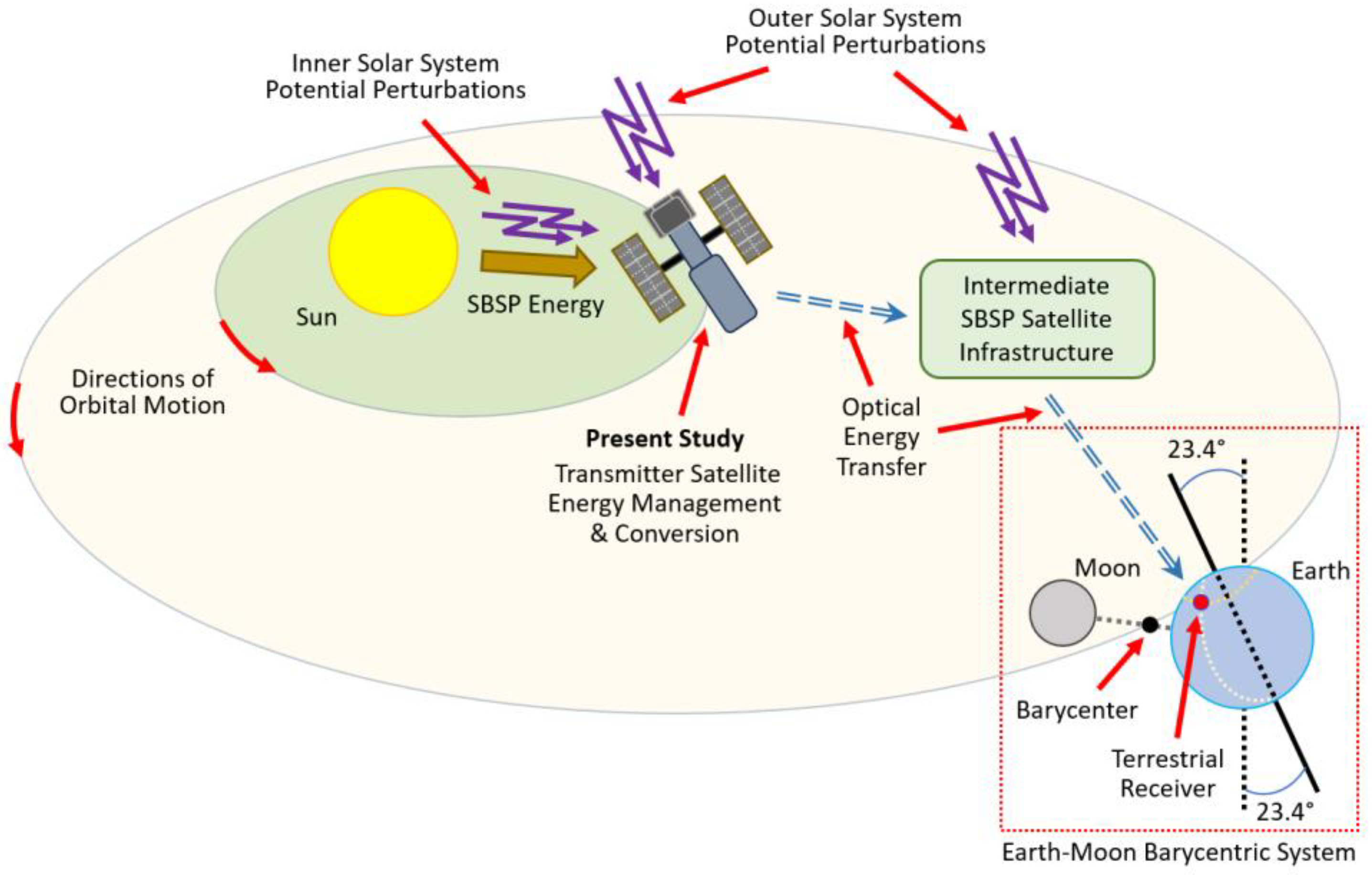
Summarizing all previously mentioned aspects, the application of this controller unit is illustrated below in
Figure 1.
The hypothetical application describes optical energy transfer over astronomical distances. Alternatively, microgrid applications could be covered due to the partial use of a similar principle for energy management circuits.
The present study considers the occurrence of intense perturbations as main constraint for conventional converter unit applicability. The proposed controller design, with the associated ASIC concept, aims to regulate SBSP energy received through solar panels at the laser transmitter satellite or at each infrastructural element receiving energy, with the resulting laser energy further transmitted through the energetic infrastructure components. Each satellite with transmission capability is considered to use energy storage units, such as battery arrays or supercapacitors.
Overall, the hypothetical hybrid BMS would consist of both computational processes, being considered as a topic for future study, as well as non-computational approaches, being the main considerations in the presently developed ASIC concept. Splitting a SBSP supply control unit from programmable memory involves implementing this solution as a mixed-signal circuit; this results in achieving the functionalities described in
Figure 2 in a single, custom-designed integrated circuit.
The purpose of functionality separation is to further improve robustness through the expected improvements in service life, as well as indirectly improving sustainability by potentially limiting the disposal, maintenance, and manufacturing of associated PCB elements. All previously mentioned aspects were considered favorable while associated with the absence of data memories in the main converter component, namely the ASIC controller unit.
Overall, two main components are required for solar energy conversion: CVCC (Constant Voltage, Constant Current) regulation as well as MPPT detection. The former concept, namely CVCC, consists of analyzing the stability of control loops in the continuous domain, as well as providing solutions to the typically used mathematical operators, such as analog or digital signal processing prototypes using electrical circuits. The latter part involving MPPT detection proceeds similarly, considering as preliminary stage the presence of a single maximum power point.
To fulfil the multiple aspects of functionality, robustness, and sustainability, the present study proceeds with functionality confirmation through regulation as well as ASIC reduction, as described in further sections.
2.1. Principles
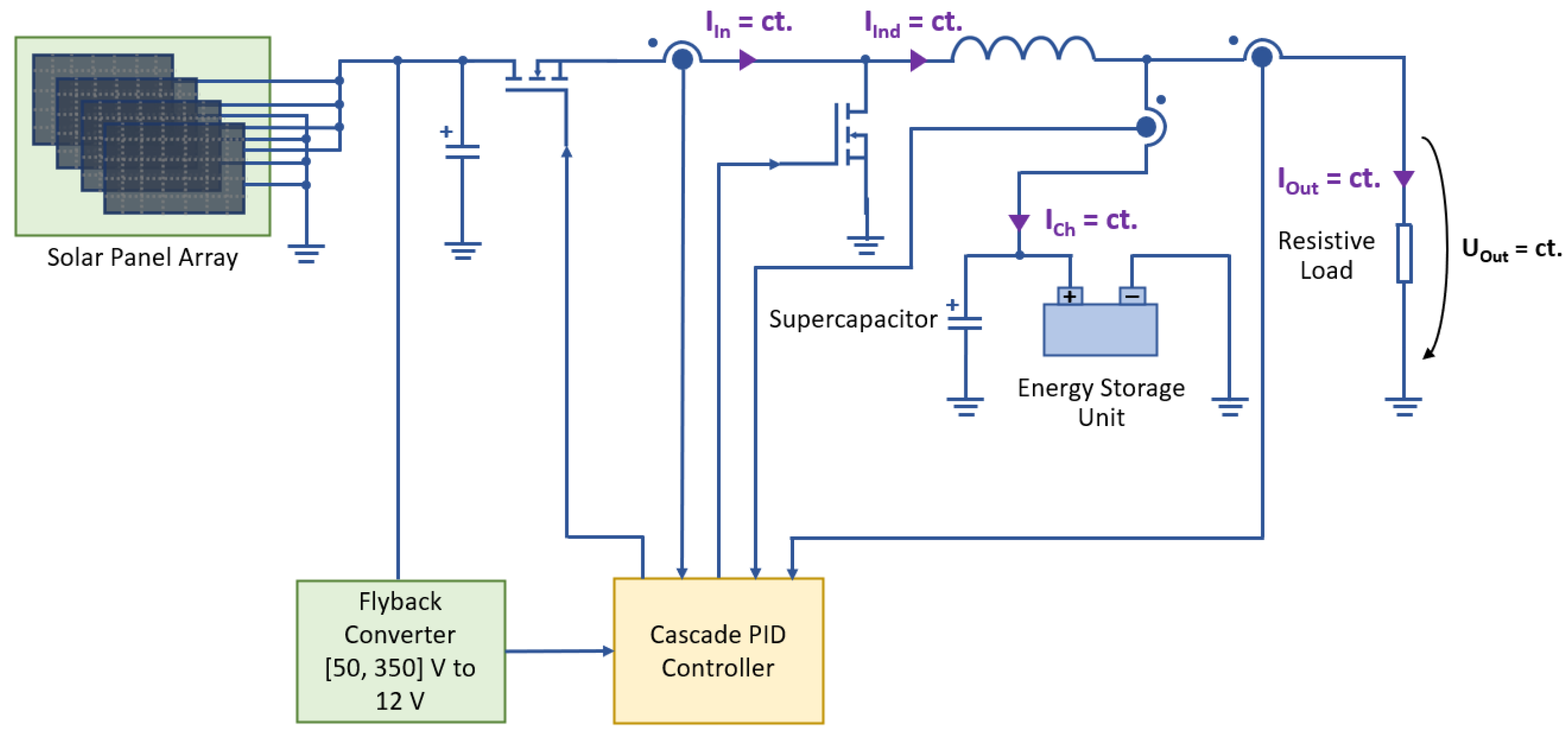
The typical application of this converter is illustrated in
Figure 3, below.
All annotations from this figure are described below:
IIn—input current;
IInd—inductor current;
ICh—charging current;
IOut—output current;
UOut—output voltage.
As described in this figure, a synchronous step-down, switched-mode power supply is implemented. A parallel array of solar panels provides the input energy, which is used to supply initial power to a flyback converter. This is necessary to regulate the charging current, starting at a voltage corresponding to a discharged battery. The usual power supply for the PID (Proportional Integral Derivative) controller is the power provided by an energy storage unit, which is converted using an auxiliary DC/DC converter. Once this auxiliary supply is enabled, the flyback converter output current is significantly reduced.
The current implementation is compatible with both Hall-effect sensors and resistive sensors for providing current feedback. However, several Hall effect sensors utilize programmable memory that is prone to data deterioration, reducing the expected operational time, which is why the case for resistive sensors was also considered.
Besides the presented step-down topology, the applicability could be extended to converters involving the absence of pole-zero boost characteristics; such DC/DC power supplies would involve forward or push-pull topologies for potential future research.
2.2. Stability Analysis
Calculating multiple transfer functions represented the first step in analyzing the regulation loop to achieve constant voltage as well as several constant currents. This circuit implements a total of five steady-state transfer functions in Equations (1)–(5):
where the transfer function is used to describe the transient and steady-state behavior of the output voltage. The following four equations analyze the current feedback paths, covering the output current:
This is followed by the input current, necessary for operating at the maximum power point:
Meanwhile, the last two feedback paths represent the inductor current, for preventing inductor core saturation by operating at constant current:
as well as charging current
for storing the converted energy while operating at nominal conditions. The operands from all previous equations are described below:
URef—reference voltage;
δCom—duty factor;
HF1,HF2,HF3,HF4,HF5—feedback paths transfer functions;
IOutFeedback, IOutSet—output current feedback and setpoint;
IInFeedback, IInSet—input current feedback and setpoint;
IIndFeedback, IIndSet—inductor current feedback and setpoint;
IChFeedback, IChSet—charging current feedback and setpoint.
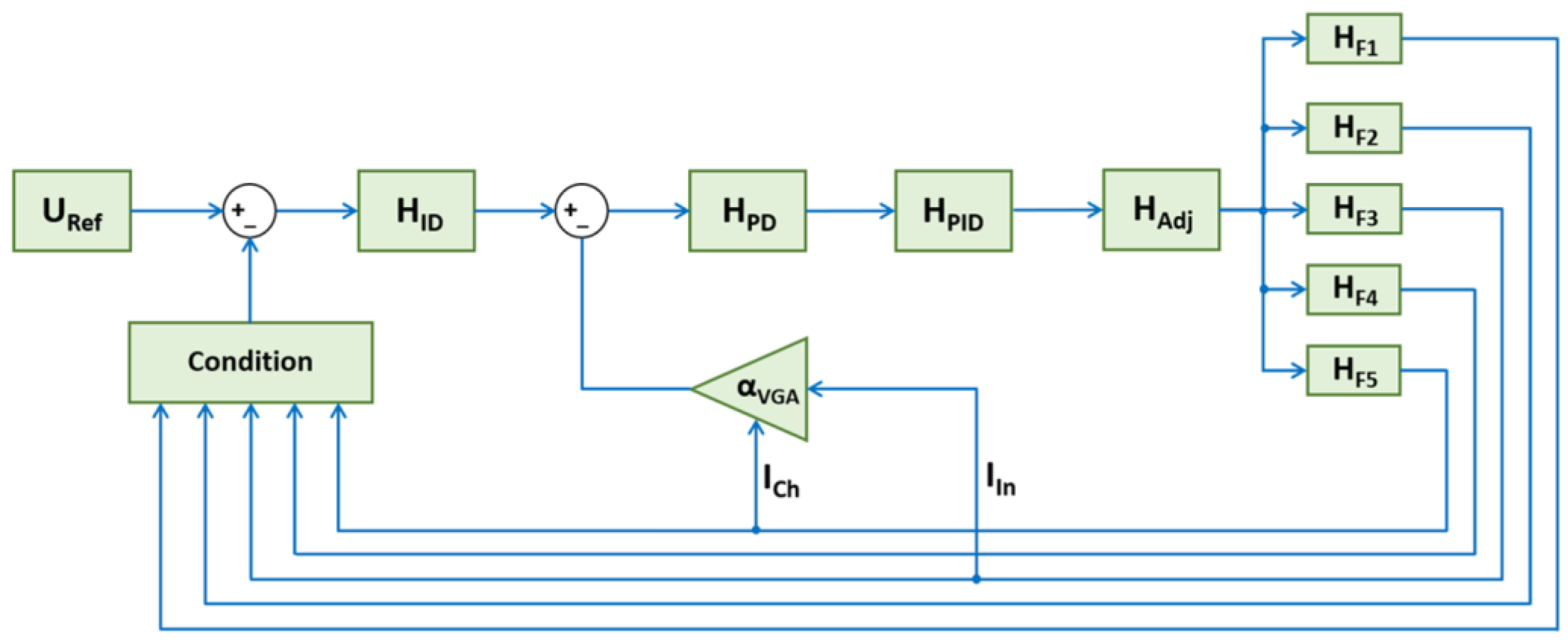
Feedback paths corresponding to the previous equations are illustrated in
Figure 4, which describes the structure of this regulator.
As described above, the control loop regulates a total of five factors using a non-linear condition based on relational operations. First, the output voltage regulation is required to prevent overcharging the energy storage unit. Next, the output current control and measurement prevent the converter from converting excessive power, as well as preventing the storage unit from over-discharging, having a similar functionality to the fourth and fifth feedback paths, namely the inductor current and charging current feedback paths. The third path, however, is used to regulate the solar panel input current.
Additionally, this controller implements a cascade PID controller with an inner VGA feedback loop to improve stability during charging current fluctuations. This innovative conditioned control improved stability and mitigated the current peak integral, as demonstrated in the following chapters.
Analyzing the stability of this system involved validating all feedback paths for this controller; the inner feedback path must not exhibit bandpass characteristics to maintain system stability for cascade feedback loops [
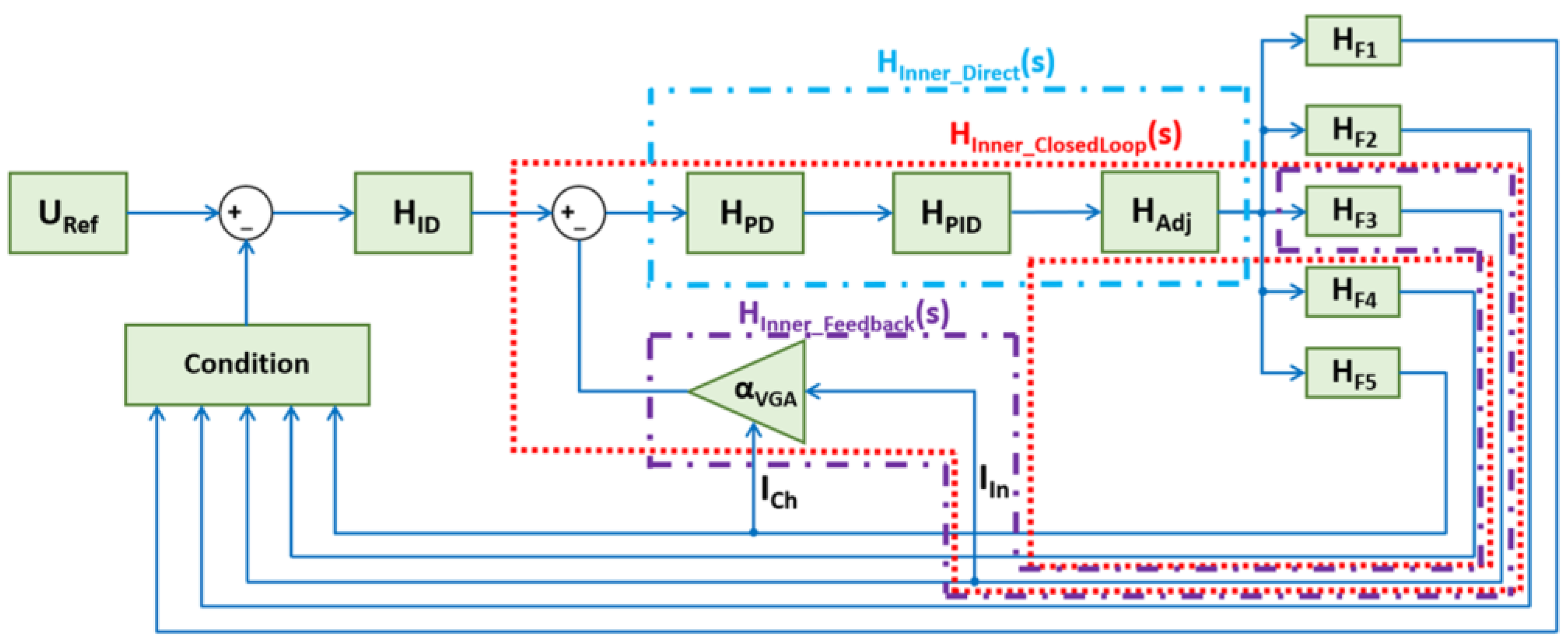
33]. The analysis continued by examining all inner controllers and their corresponding inner feedback propagation paths. Next, the inner feedback to outer controller feedback paths were analyzed, followed by simplifying the inner regulation loop based on Equation (6):
having the closed-loop, direct, and feedback transfer functions described below in
Figure 5.
Based on the previous equation, the inner closed-loop transfer function was calculated by considering the control voltage transformation into a duty factor, followed by obtaining the input current feedback voltage based on the duty factor, the current-to-voltage gain transfer function, and the VGA gain transfer function. The charging current path was not considered in the mathematical model due to the non-linear conditioning.
Following the simplification of the inner loop, the study analyzes the stability of all five transfer functions, as described in the next section.
2.3. Stability Results
The stability analysis considers as nominal operating conditions the factors from below:
Input voltage: 100 V.
Output voltage: 28.6 V.
Inductance: 8.2 uH.
Capacitance: 4.7 F.
Inductor ESR (Equivalent Series Resistance): 5 mΩ.
Duty factor: 30%.
Capacitor ESR iteration interval: [0.001, 100] Ω.
Output current iteration interval: [0.1, 1000] Amperes.
Two iterated factors were considered, having the most important influence on the system phase margin, namely the output resistance and capacitor ESR. All analyzed feedback paths start from the outer controller, the integrative-derivative controller, and evaluate the phase shifting until reaching the subtraction operator.
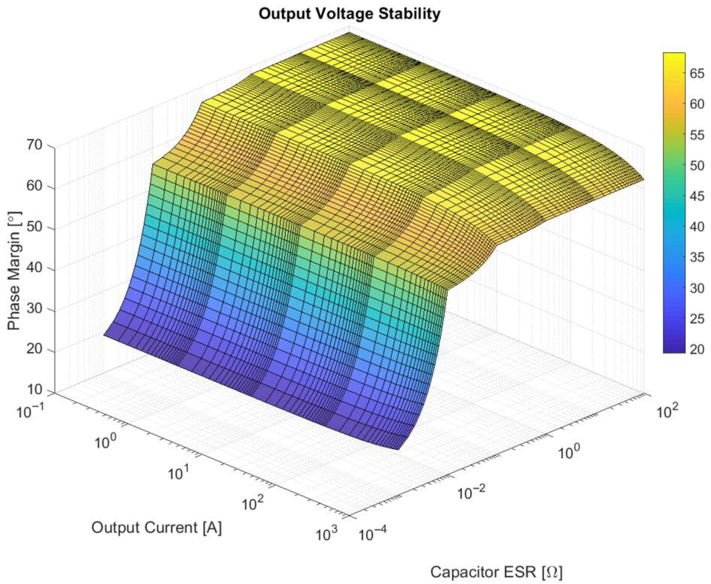
The first evaluated factor is represented by output voltage regulation, as described in
Figure 6.
The phase margin analysis reveals a significant decrease in stability when the output filter capacitor ESR reaches values below 1 milliohm. Mostly, stability is affected by this factor, with the influence of output load occurring only at high output currents. However, these two scenarios are hypothetical. Therefore, the system is considered stable in the output voltage feedback path.
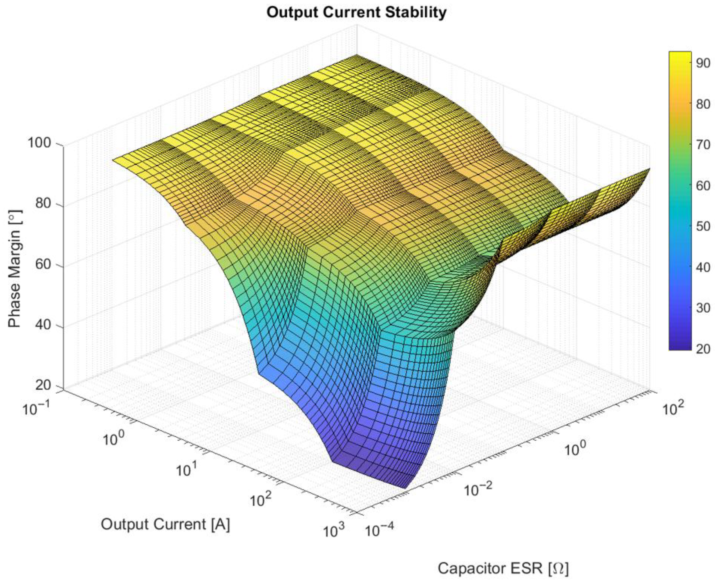
The next factor evaluated for proving system stability is represented by the output current phase margin, as shown in
Figure 7, below.
In this case, both the converter capacitor ESR and the output resistance influence the phase margin. The stability analysis also reveals a reduced phase margin, below 20 degrees, for hypothetical scenarios, such as capacitors close to ideal and intense output currents, corresponding to significantly reduced load resistance.
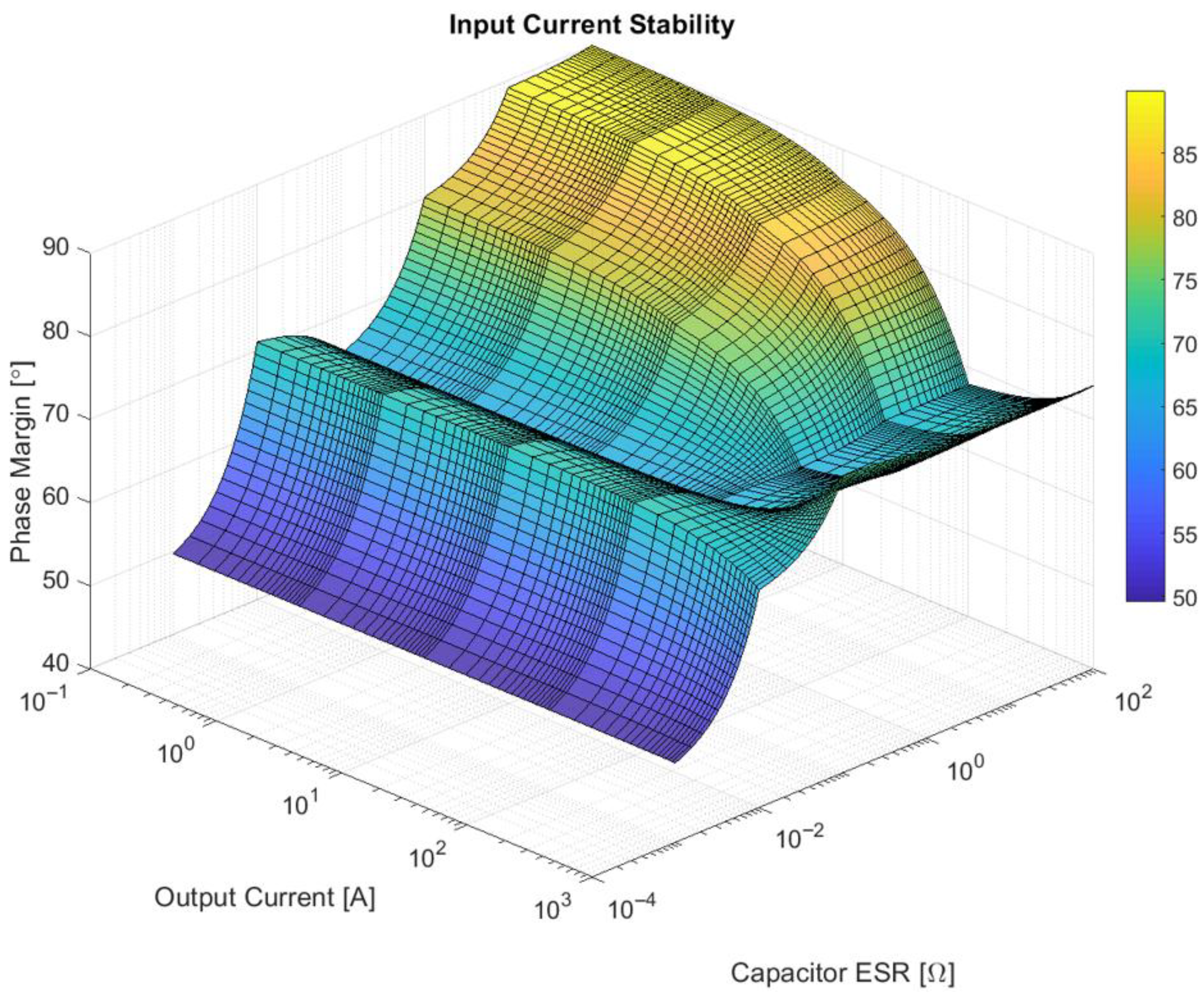
The third factor influencing system stability is represented by the input current. This current regulation is required to maintain the operation of this switched-mode power supply close to the maximum power point, having the phase margin plot illustrated below in
Figure 8.
Mainly, the phase margin is influenced similarly to the output current feedback stability. A significant influence occurs at reduced capacitor ESR, where the phase margin decreases below 50 degrees. In this case, the output load variation has a limited impact on phase margin variation, in a range of approximately 40–50 amperes as the output current.
The input current analysis involved linearizing the system by compensating for its internal dependency to obtain a linear, time-invariant system. Therefore, a dummy value for duty factor was required to conclude system stability, based on Equation (7):
to obtain
IIn, the input current, as a function of the inductor current,
IInd, over the control duty factor. This required the use of the terminal voltage difference for elaborating the inductor current, as shown in Equation (8):
where the input and output voltages,
UIn and
UOut, respectively, were also considered for obtaining this approximation, operating at a dummy duty cycle of 30%, previously mentioned as test conditions.
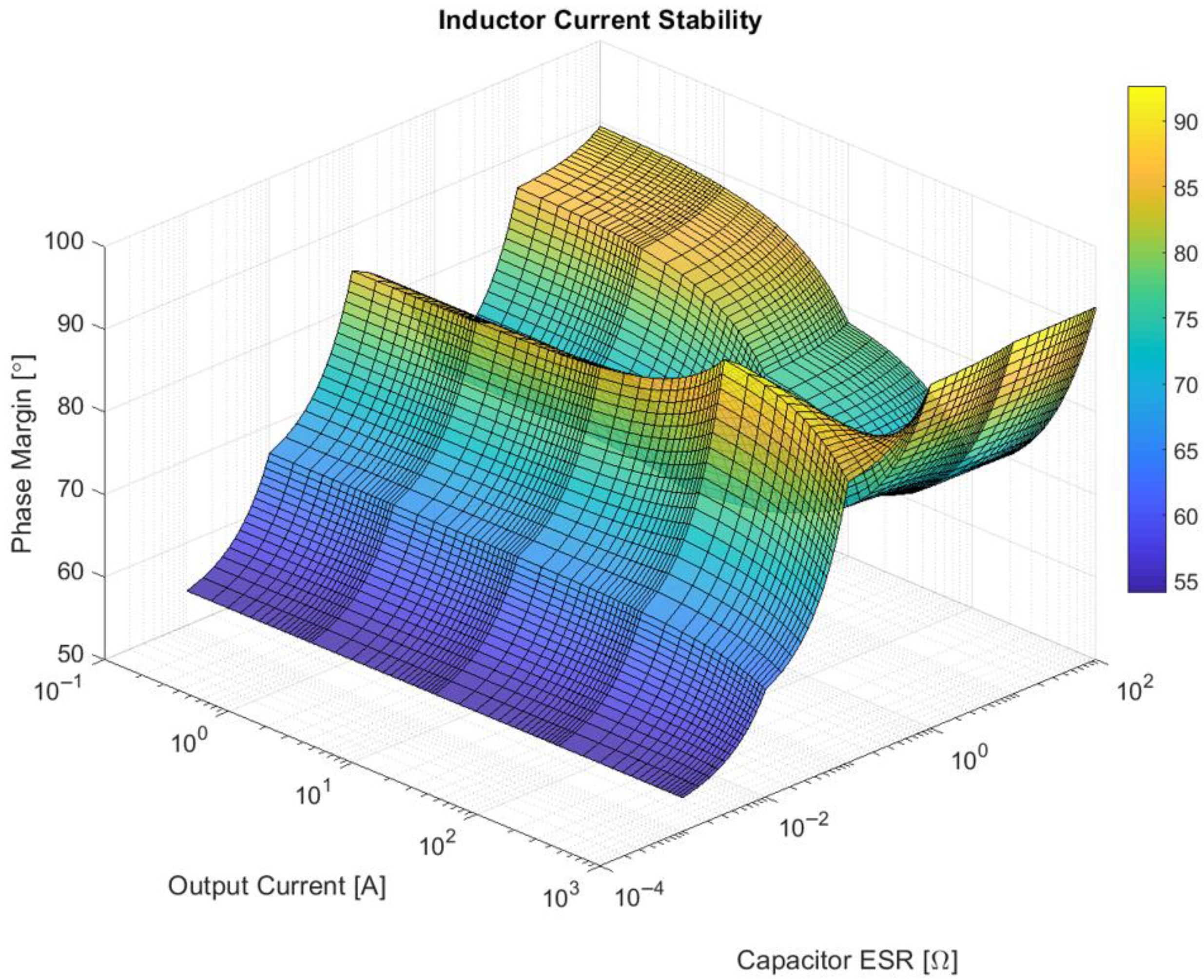
Further analyzing the system stability involved evaluating the inductor current phase margin, as described in
Figure 9.
In this case, for average to high capacitor ESR values, the system phase margin increases above 90 degrees at high output currents, indicating a possible short-circuit operation. By analyzing lower currents, a region where the phase margin approaches 90 degrees can be identified. For capacitor ESR values approaching the ideal case, the phase margin decreases to approximately 55 degrees.
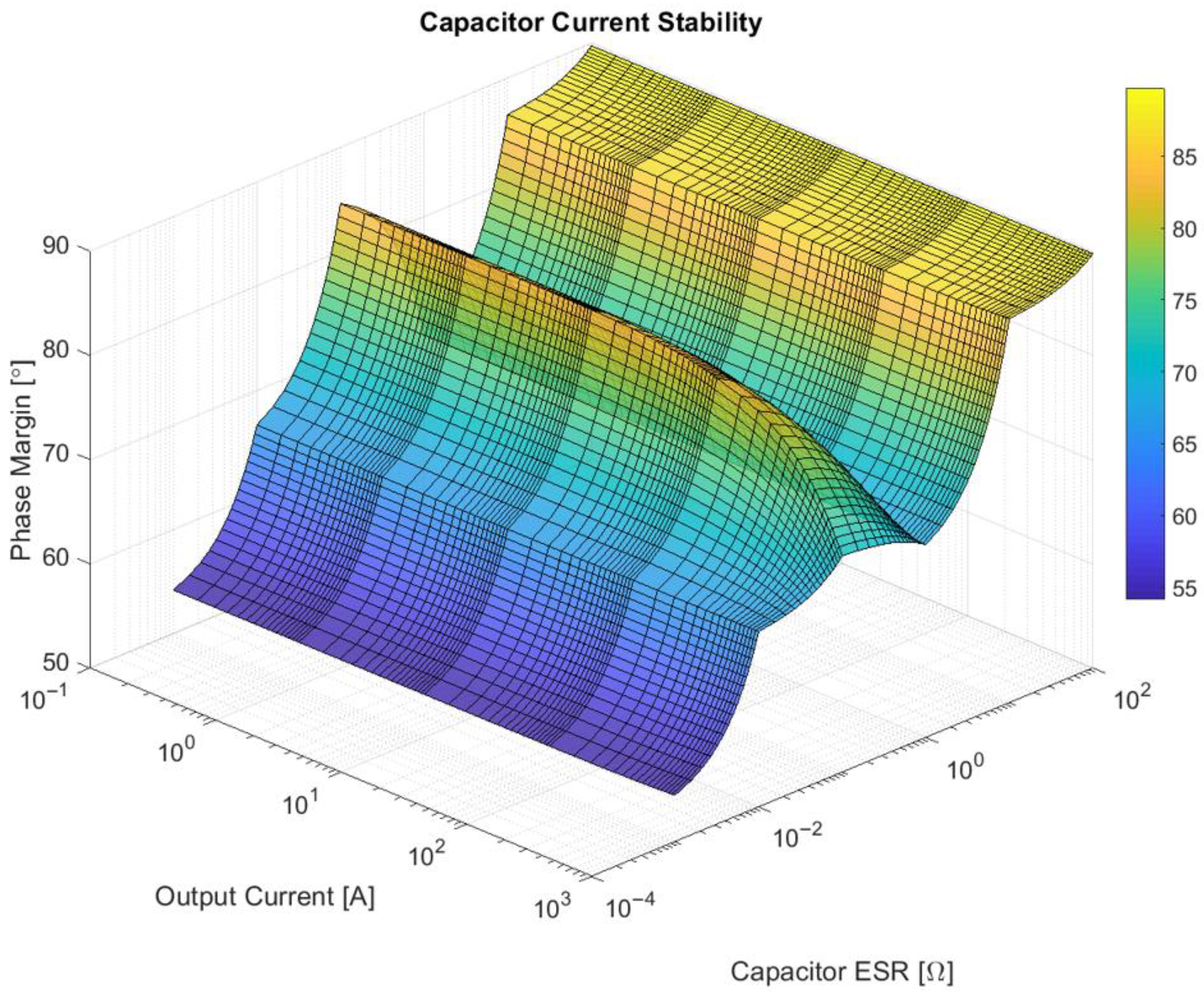
The last factor required to cover the stability analysis is represented by the capacitor or charging current, as described in
Figure 10.
The system stability analysis shows, in this case, a similar value of 55 degrees for operating at ideal capacitor ESR values. Mostly, the output current has a reduced influence on the phase margin values, and only during short-circuit operation does the phase margin slightly decrease at loads corresponding to 1000 amperes or output resistances close to 30 milliohms. At high capacitor ESR values, an increase in phase margin of approximately 90 degrees can be observed, having the region for this phase margin value at approximately 0.5 ohms, corresponding to the capacitor ESR.
By analyzing the previously mentioned factors for system stability, relevant operating cases were examined, and the system is considered stable. By further analyzing the system stability, multiple factors, such as converter inductance or minimum capacitor value, have shown a permitted tolerance in shifting from the nominal operating conditions. The previously mentioned supercapacitor connected in parallel to the energy storage unit is required to maintain system stability in the event of the energy storage unit malfunctioning.
Equation (9) was used to mathematically obtain the transient regime values for closed-loop transfer functions:
The steady state value was obtained based on Equation (10):
and the output variations, as well as the integrity percentage ratios given by evaluating the system. The theoretical values for operating close to the nominal conditions are specified in
Table 1, below.
The percentages from this table represent a basis for all simulations from the next chapter and denote the presence of a pole very close to the origin from the pole-zero graphical representations of all transfer functions. Several variation values were given relative to a change of 1 volt in reference voltage, while also specifying the ratios for voltages associated with currents corresponding to the mathematical model implementation.
This pole allows for the integrity of all factors to be maintained very close to the ideal case, with the single limitation arising from the common residual terms in the closed-loop transfer function denominator. This limitation occurs with each LTI system due to the loop closing, resulting in a slight shift from the ideal steady-state value.
Following the system analysis, the electric circuit designs for various functions were covered in the next section, providing the possibility to implement complex calculations.
2.4. Substitutions for Complex Functions
In this section, commonly used mathematical operators were implemented as electric circuits instead of computations. The circuits were developed using high-speed operational amplifiers, allowing the possibility to transition signals between the analog and digital domain.
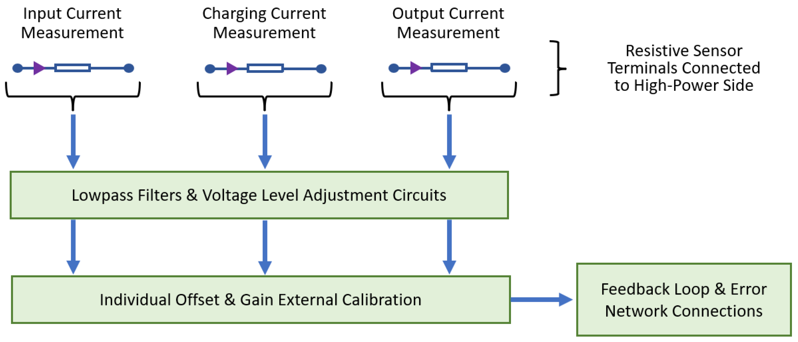
Resistive current sensors require a bidirectional capability to distinguish between charging and discharging regimes. However, this only applies to the charging current but due to the inductor current calculation, this capability was implemented for all three measured currents:
Input current;
Charging current;
Output current.
All three measurement bridges were illustrated in
Figure 11, below.
Considering a high precision, with 0.1% tolerance, approximately 6.4 amperes are expected as variation in current regulation, a difference occurring between paired branches. However, the dynamic characteristics cancel each other out due to the subtraction operator.
The previously described circuit block diagram implements only three measurement points to obtain four currents, namely the input current, inductor current, charging current, and output current. From all these four factors, only the inductor current is not measured, to avoid high fluctuations in voltage readings. Therefore, to calculate this current, multiple summations and subtractions were used in mathematics to obtain the raw value, followed by further processing. This indirect inductor current measurement circuit uses three sensors to measure four currents, minimizing the required number of components.
2.5. Multiple Feedback Paths Regulation
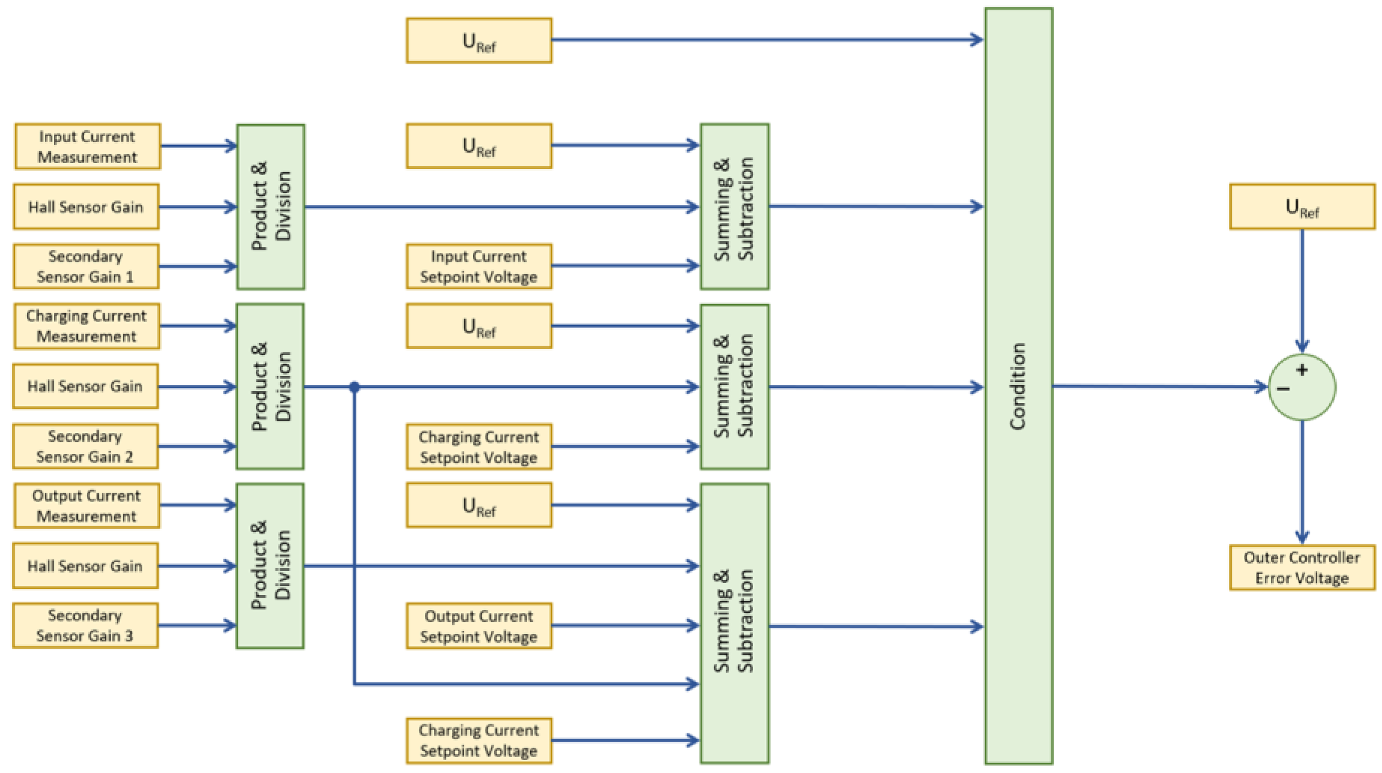
Based on the previously described mathematical procedure for obtaining the inductor current, a simplified procedure was used to obtain the remaining raw current readings and add the reference voltage to these values. This reference voltage was required for implementing the multiple-path regulation described in
Figure 12.
Obtaining all currents, including the inductor current, required multiple summation, subtraction, product, and division operations to determine the accurate value. Following this processing, the currents were read, and a conditioning operator was used to provide the loop feedback in order to increase or decrease the converter command.
Because several non-linearities can be identified, each factor not taken into consideration, besides the actual analyzed factor, can be ignored when evaluating system stability, such as the reference voltage or non-linear conditional operator. For analyzing the stability of this path, the superposition principle was used, as described in Equation (11):
describing the system response for linear systems as the sum of individual responses. Thus, to prove the entire system’s stability, each of the individual feedback paths were previously evaluated.
For implementing the summation and subtraction circuits, Millman’s theorem, described in Equation (12), was used:
Here, the variables denote the following:
Vx—voltage at the intermediate point influenced by all other voltages;
Vk—parallel generator output voltage, for k from 1 to n;
Rk—parallel generator output resistance, for k from 1 to n;
n—total number of parallel generators.
Operational amplifiers can be considered as ideal voltage sources for designing addition or subtraction circuits.
2.6. Maximum Power Point Tracking
The maximum power point detector adjusts the duty factor to maintain a maximum power conversion efficiency at the input side, namely for solar panels. The present study implements this tracking function as an additional circuit to provide the limit value for input current.
A local-optimum peak power detection circuit was implemented for this application, having its schematic presented below in
Figure 13.
This circuit constantly adjusts the available output current using multiple flags, required for initializing the charge pump, detecting wind-up or input voltage absence, as well as detecting a decrease in input power. Both inputs from this flip-flop, data, and clock, are conditioned in such a way that after reaching the steady state, the power decrease flag becomes dominant. Enabling the power decrease flag requires the present power product to be lower than the past power product. The 74163 integrated circuit provides the option to be used as a free-running counter, as configured for this circuit, with three defined states for detecting a decrease in input power.
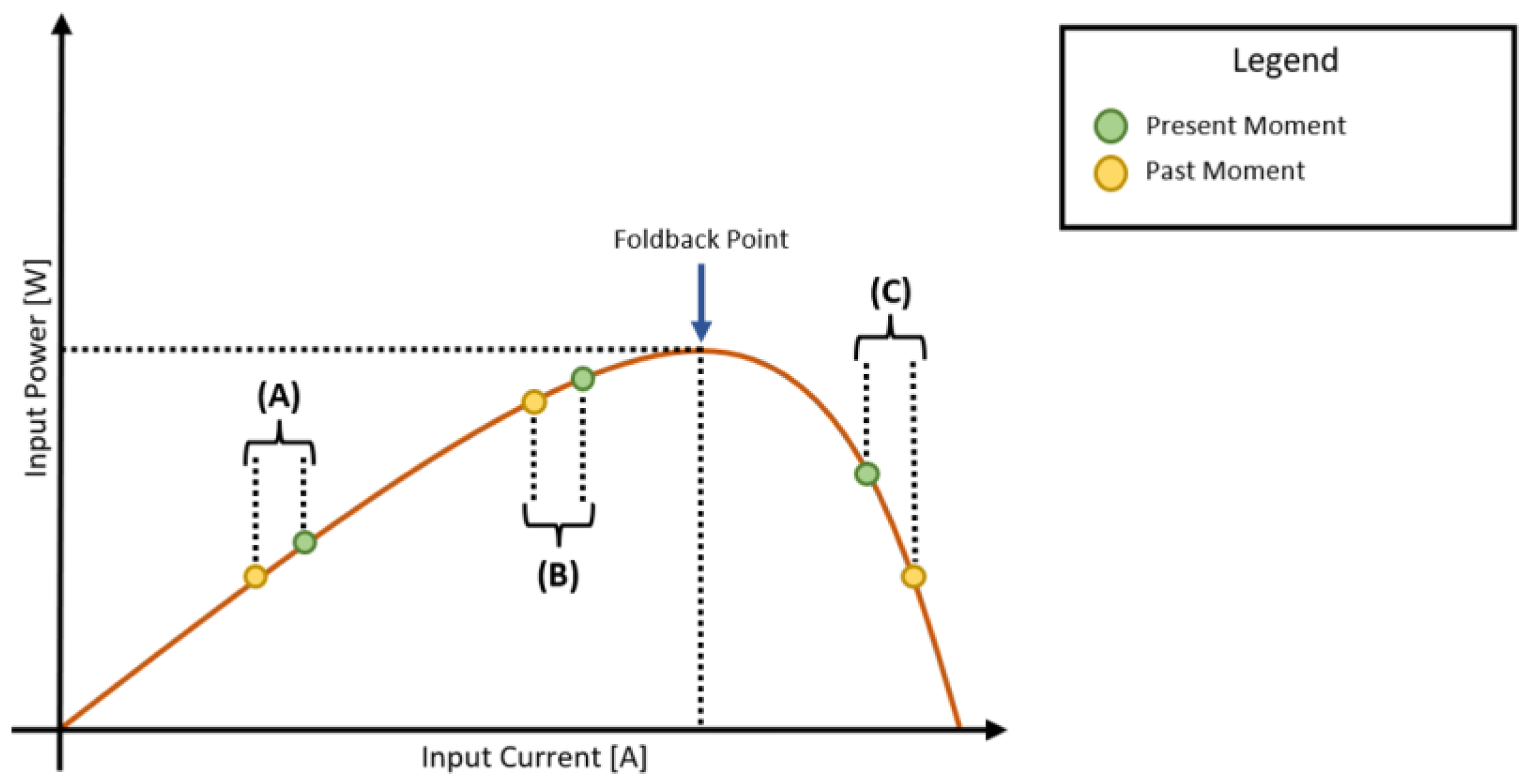
The complete functionality of this tracking circuit implements the detection of an evenly illuminated or shaded solar panel array, presenting a single maximum power point, as described in
Figure 14.
For cases A and B, the regulator increases the available current while reading the feedback current and calculating a power voltage product. For case C, as previously described, the detector toggles the direction of the input current search. The intermittent switching between search directions maintains the current setpoint from this regulator close to the maximum efficiency point.
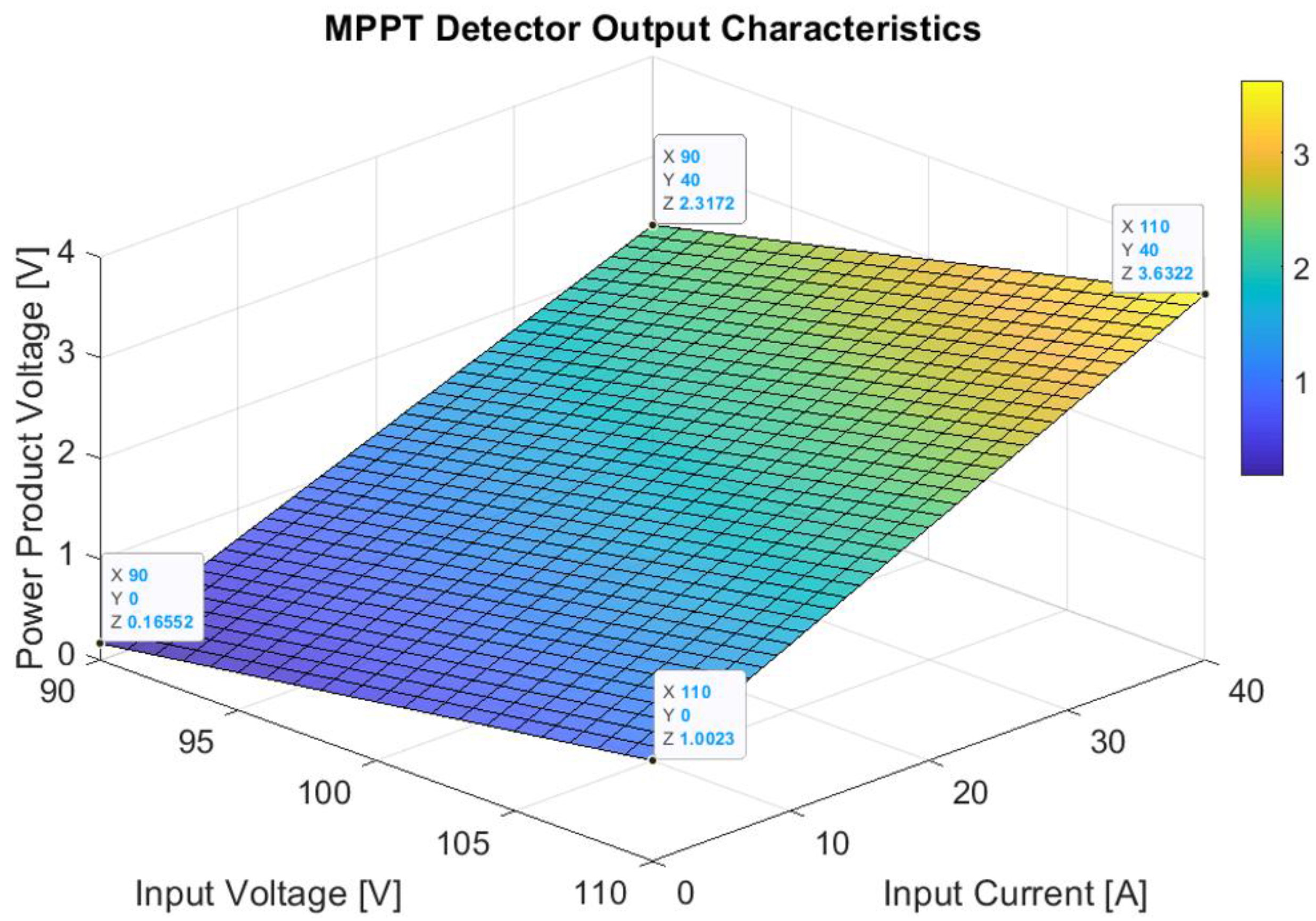
Theoretically, the transfer characteristics for this design result in the limits presented in
Figure 15.
The voltage range extends from 0.16 to 3.63 volts, covering the nominal operating conditions. Below the minimum voltage, the available input current is maintained at zero. This voltage product also depends on input current feedback.
The following section covers the integration of additional functionalities for this switched-mode regulator, enabling compatibility with multiple types of energy storage units.
2.7. Additional Functionalities for Grid Integration
Several protection mechanisms were required to ensure compatibility with lead–acid and lithium-ion battery banks. First, the operating temperature was restricted to approximately 7 °C as the lower limit and 40 °C as the upper limit. The defined derating characteristics of the charging current are described in
Figure 16.
Besides the current derating, a diagnosis error network was also implemented to abruptly interrupt the converter operation, lowering the duty cycle to zero percent. The implemented diagnostic events are listed below:
Overvoltage error;
Thermal runaway;
Over-discharge error.
To implement the entire diagnosis network, an error signal feedback was required to be provided as input to a summing circuit, which implements the logical “or” function between all possible errors.
Having covered these functionalities, the next chapter continues with the analysis of simulation results.
3. Results
Following the theoretical implementation of the two main parts, the regulation loop and MPPT circuit, this chapter presents the simulation results. Furthermore, following the analysis and calibration of this DC/DC converter, the operating conditions are described in
Table 2, below.
All values presented above specify the limits for multiple factors in various cases. A null input current reference will be provided if the input voltage decreases below 90 volts. Due to the internal dependency when designing the VGA controller, a dummy duty factor was used, and its variation was analyzed to determine system stability, the reason for which being that the value should be close to this specification when this alternative feedback path is used. The output load resistance provides only an approximate range for operation, while the inductor must be as close as possible to the specified value for all inductor current values. A minimum capacitance is required to maintain system stability; however, an indefinite number of parallel battery packs can be connected at the output.
Based on the information previously described, the mathematical model results are illustrated in
Figure 17.
All highlighted sections from this schematic are explained below:
1—switched-mode DC/DC power supply model;B
2—control loop, receiving the error voltage as input;
3—feedback voltage calculation;
4—input current estimation, resulting in internal dependencies;
5—converter parameter definition;
6—delayed turn-on signal;
7—resistive load variation test case stimulation;
8—input current limitation test case stimulation.
Due to the internal dependencies that occur, a single test case is insufficient to cover all possibilities, given the simulator’s approximations. A loss of accuracy happens during resistive load variation when the input current is also restricted; this precision loss was analyzed and associated with internal dependencies and nonlinearities. Therefore, the following section covers converter simulation in two different scenarios, operating at variable load and input current limitation.
3.1. Regulator Simulation
Simulating a MATLAB/Simulink CVCC mathematical model required, as a first step, defining the test case, parameters, and test conditions. No perturbations were considered to occur and propagate EMI through various circuit paths during simulation. Therefore, all simulation factors for proving stability during output load variation are specified below:
Test case—variable output load;
Input voltage—100 V;
Output voltage—28.6 V;
Initial energy storage unit voltage: –10 V;
Inductance—8.2 uH;
Capacitor—4.7 F;
Inductor ESR—5 mΩ;
Capacitor ESR—4 mΩ;
Duty factor—30%;
Maximum inductor current—47 A;
Maximum charging current—17 A;
Maximum input current—10 A;
Load resistance—variable.
All test cases in this section use reduced VGA feedback, which has a lower influence on simulation results. Further non-linearities would limit the simulation outcome by forming a bandpass characteristic, requiring special control signals that would induce additional non-linearities. This is why the VGA feedback path was analyzed separately using Bode characteristics to confirm stability.
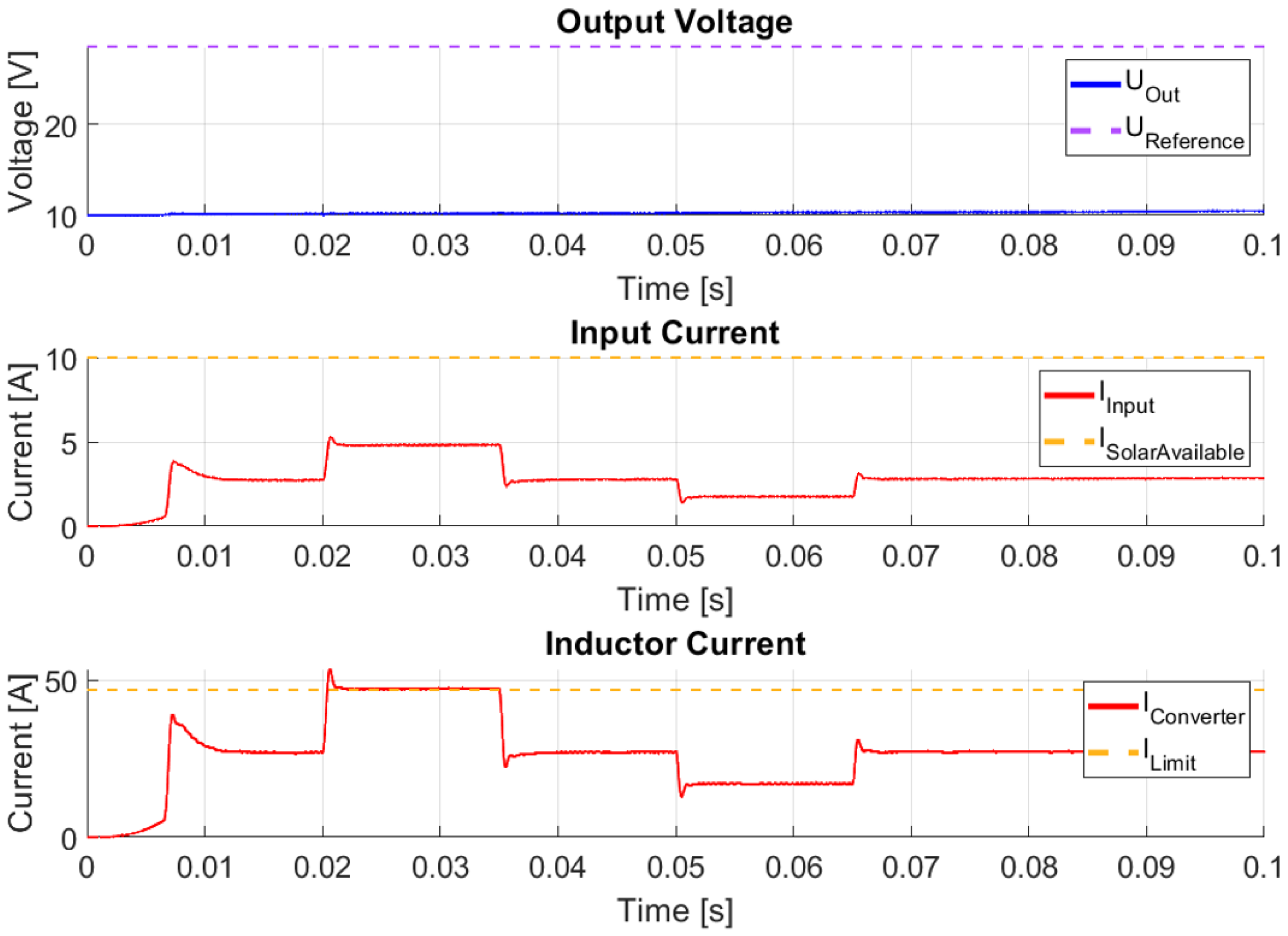
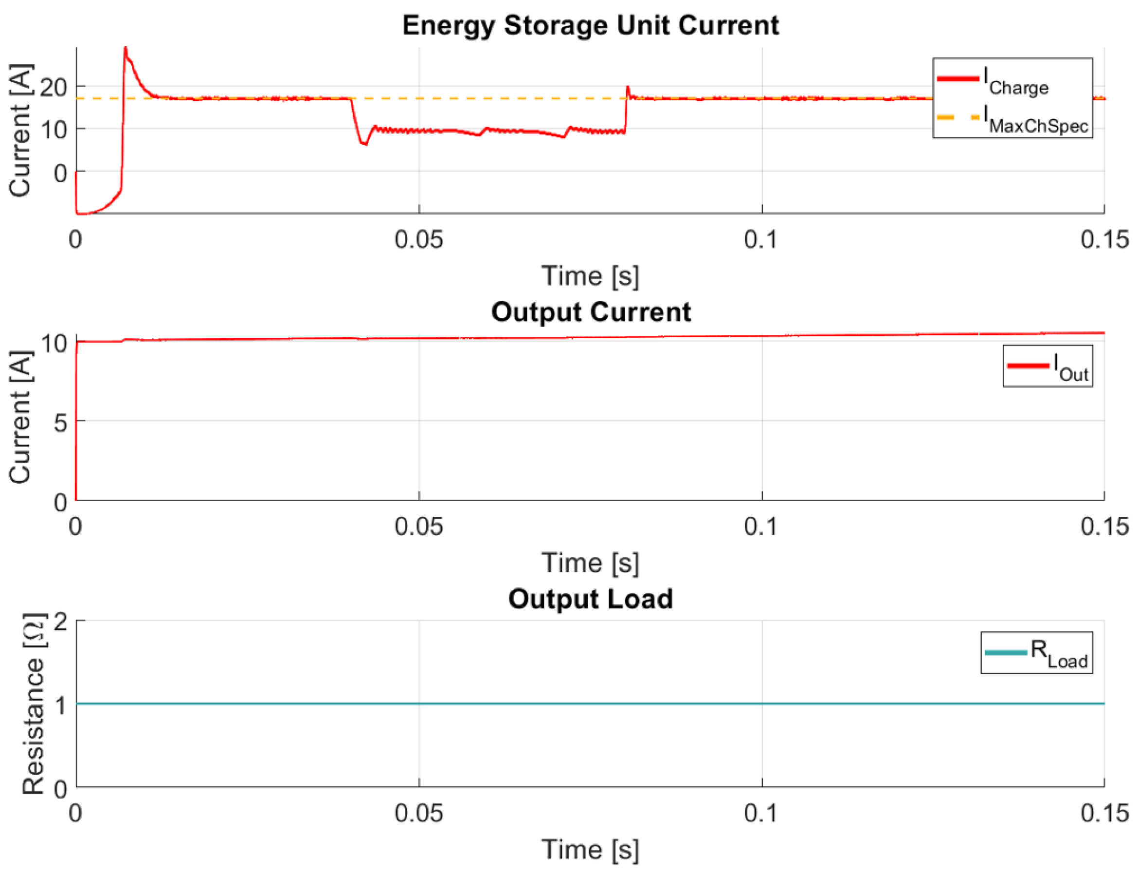
Based on the previously defined parameters and variables, the simulation result is presented below, in
Figure 18.
In this case, the output voltage slowly increases towards its reference value while the input and inductor currents change as a function of the output resistance. A limitation in the inductor current occurs, confirming the correct implementation of the current calculation based on different sensors. The additional simulation results associated with this test case are covered in
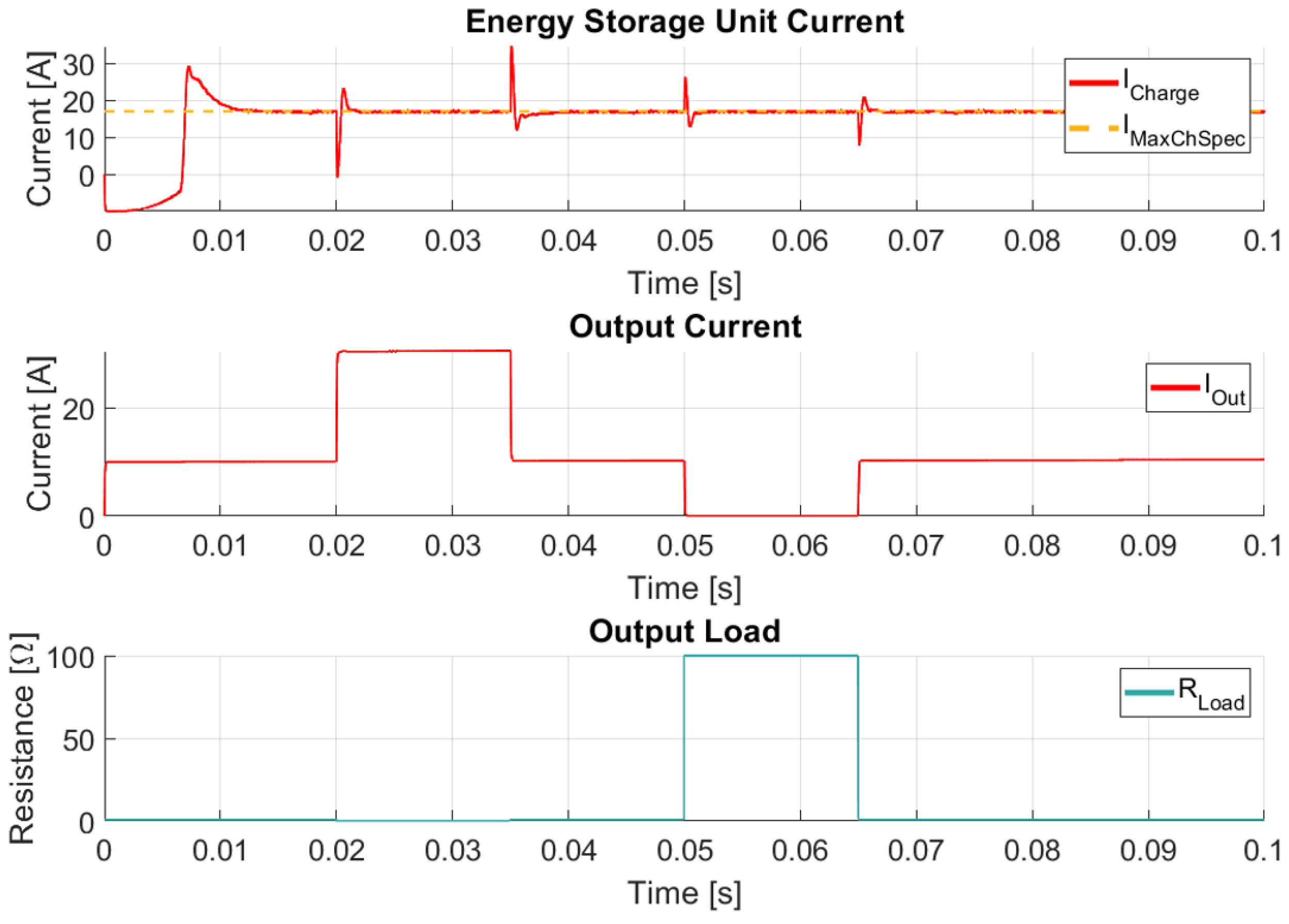
Figure 19.
In this figure, the variation in output load is also illustrated. The convergence of the charging current to its nominal value can be observed as the output current changes in response to the output resistance.
The next test involves evaluating the converter stability during input current limitation, having several parameters adjusted compared to the defined test conditions:
Test case—input current limitation;
Maximum input current—variable;
Load resistance—constant.
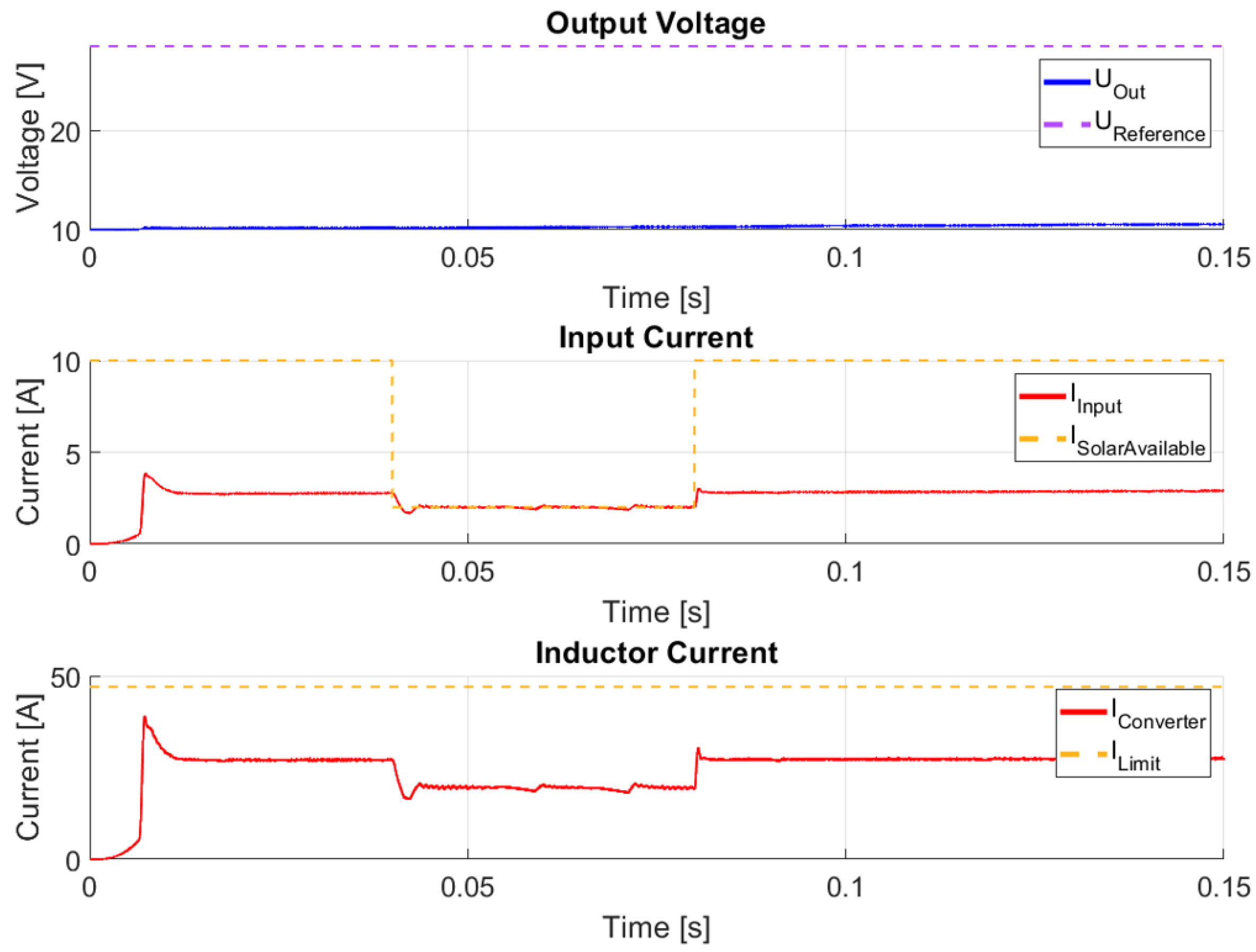
Following the change in these factors, the simulation result from
Figure 20 corresponds to restricting the input current, operating in a similar condition to maintaining the maximum power point.
This result highlights the limitation of the inductor current by restricting the available input current. The solar panel output current shows a decrease over a certain time interval, and the input current converges to this value with minimal fluctuations. Additional results are provided below, in
Figure 21.
A restriction in the charging current of the energy storage unit is also observed, confirming the stability of input current regulation. The fluctuations occurred due to simulating a time-invariant system with internal dependencies; several simulator approximations were necessary for solver convergence and to obtain the presented results.
Additionally, the results presented in this section, beyond proving stability test cases, continue to demonstrate transient performance improvement.
3.2. Current Peak Integral Reduction
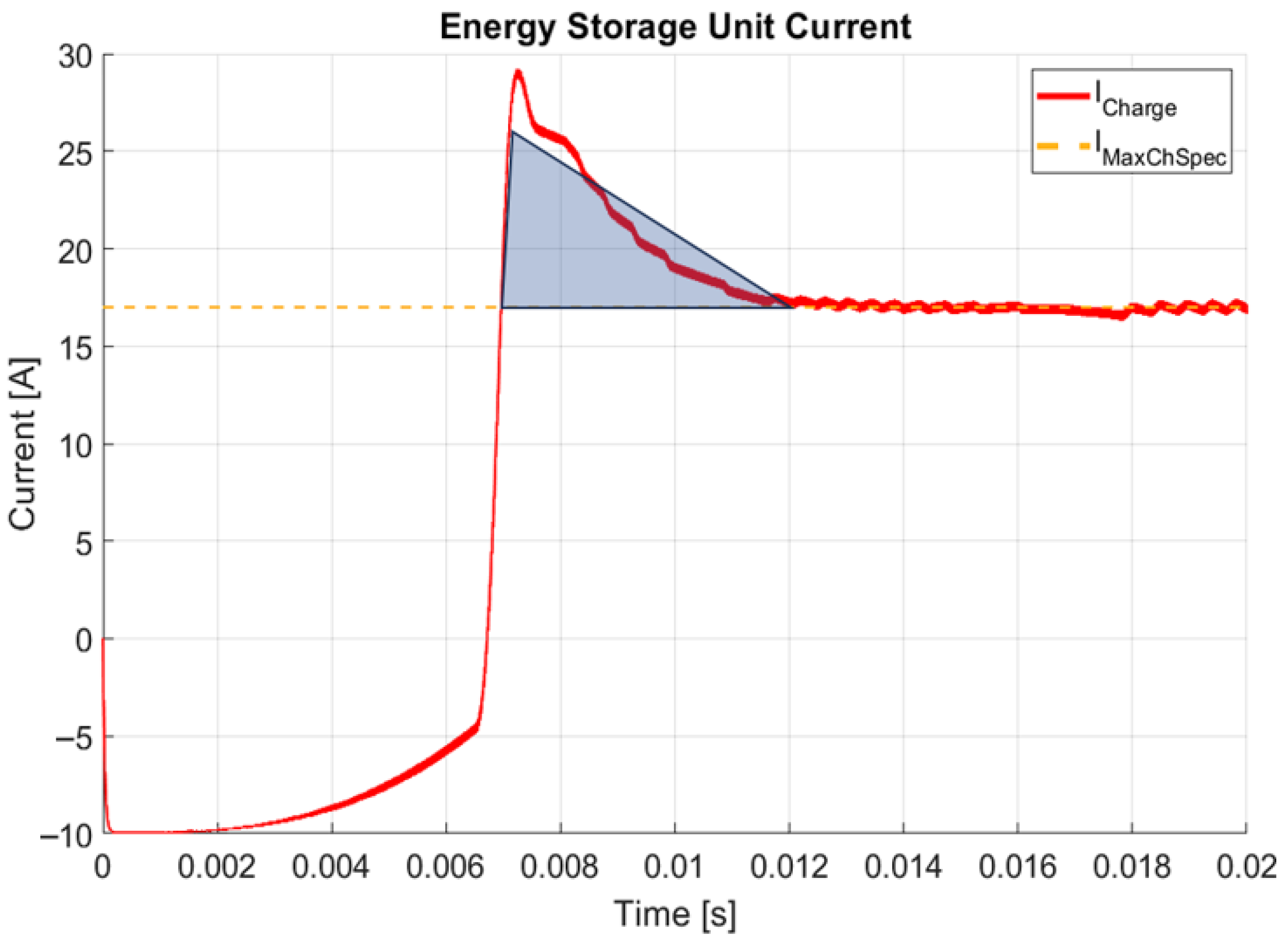
Certain battery packs allow for limited variations in charging current. The VGA inner controller feedback was configured to reduced gain followed by increased gain. The loop was evaluated for improving transient performance, and the result from a previously defined test case, operating at variable load and nominal operating conditions, is presented separately in
Figure 22 for the charging current.
In this figure, the blue triangle approximation represents the current peak integral measurement, yielding 23.75 amperes/milliseconds. For this result, a negligible VGA gain was set, corresponding to the previously described first test case. By enabling the VGA feedback path and implementing a fixed input current gain, system stability is improved, resulting in increased transient performance, as shown in
Figure 23.
In this figure, the new current peak integral measurement is highlighted in blue, while a purple triangle denotes the previous result. In this case, the VGA feedback path improved the current peak integral from 23.75 to 18.75 amperes/milliseconds, resulting in a 21.05% reduction. By analyzing system stability, it can be seen that an improvement in phase margin also occurred, as presented in
Table 3.
The VGA feedback path improves phase margin, as described above, with the single exception of the output current, for which stability is reduced. The other four factors, however, present an improvement in stability.
All previously presented results demonstrate the successful implementation of this switched-mode power supply model, which improves service life, sustainability, and system stability by utilizing a gain controller on the inner feedback path. This controller, implemented as a fixed gain, could be further improved by conditioning based on the charging current, enabling it only during specific time frames to avoid bandpass characteristics in the inner feedback loop and thereby decrease stability.
The following section presents the simulation for an MPPT model, which is implemented based on the previously described theoretical analysis.
3.3. MPPT Circuit Simulation
For simulating the maximum power point tracking circuit, a hypothetical non-ideal generator was used for modeling the behavior of a local maximum in input power characteristics. This generator powers a one-ohm load and operates as a voltage source, having a series resistance of 10 ohms. The generator model was implemented in MATLAB while the complete functionality of the MPPT circuit was developed as a mathematical model in MATLAB/Simulink, considering no external EMI propagation through circuit paths. All other test conditions are listed below as approximate values:
Available input current voltage derivative—0.14 V/s, equivalent to 7 A/s;
State machine refresh frequency—62 Hz;
Voltage product sample circuit time step—1 ms;
Memory circuits time constants—180 μs;
Input voltage—100 V.
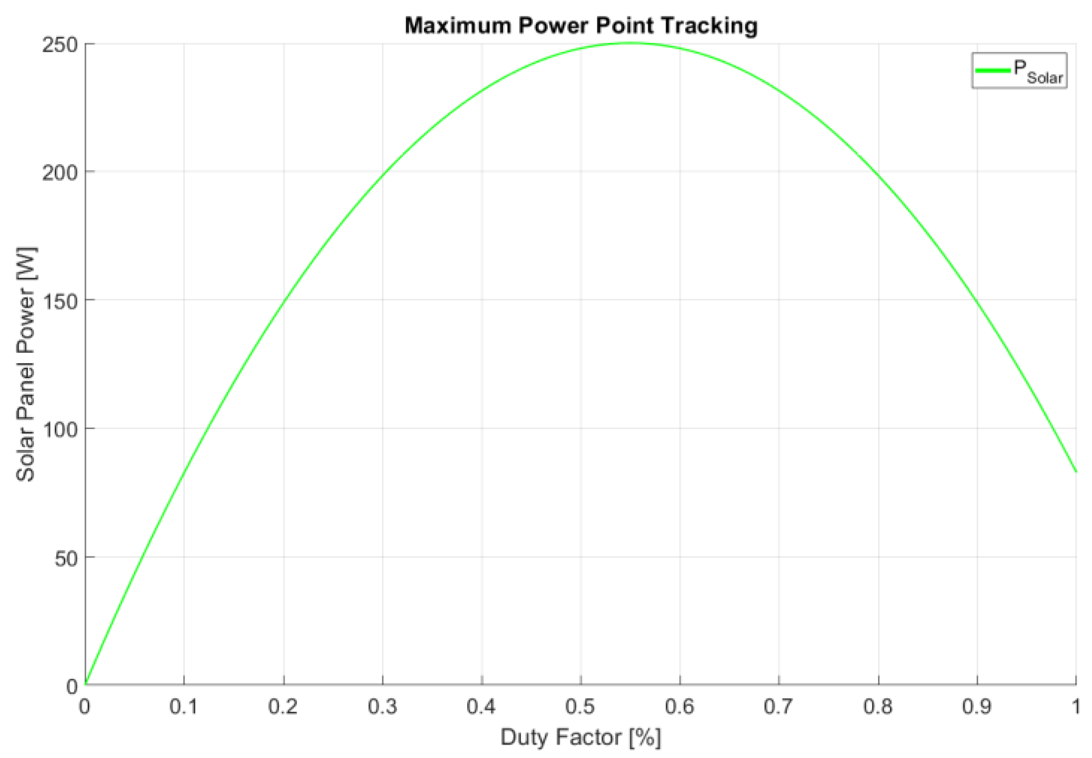
An initial analysis of the input power characteristics of the hypothetical non-ideal generator is presented in
Figure 24.
The analytical approach considers the operation of an ideal step-down converter, having its switching element connected between the input side voltage generator and the output load. At the maximum power point, the resulting output current is 5 amperes at a 55% duty factor, while providing 50 volts as measured at the input side, and also delivering 250 watts as input power.
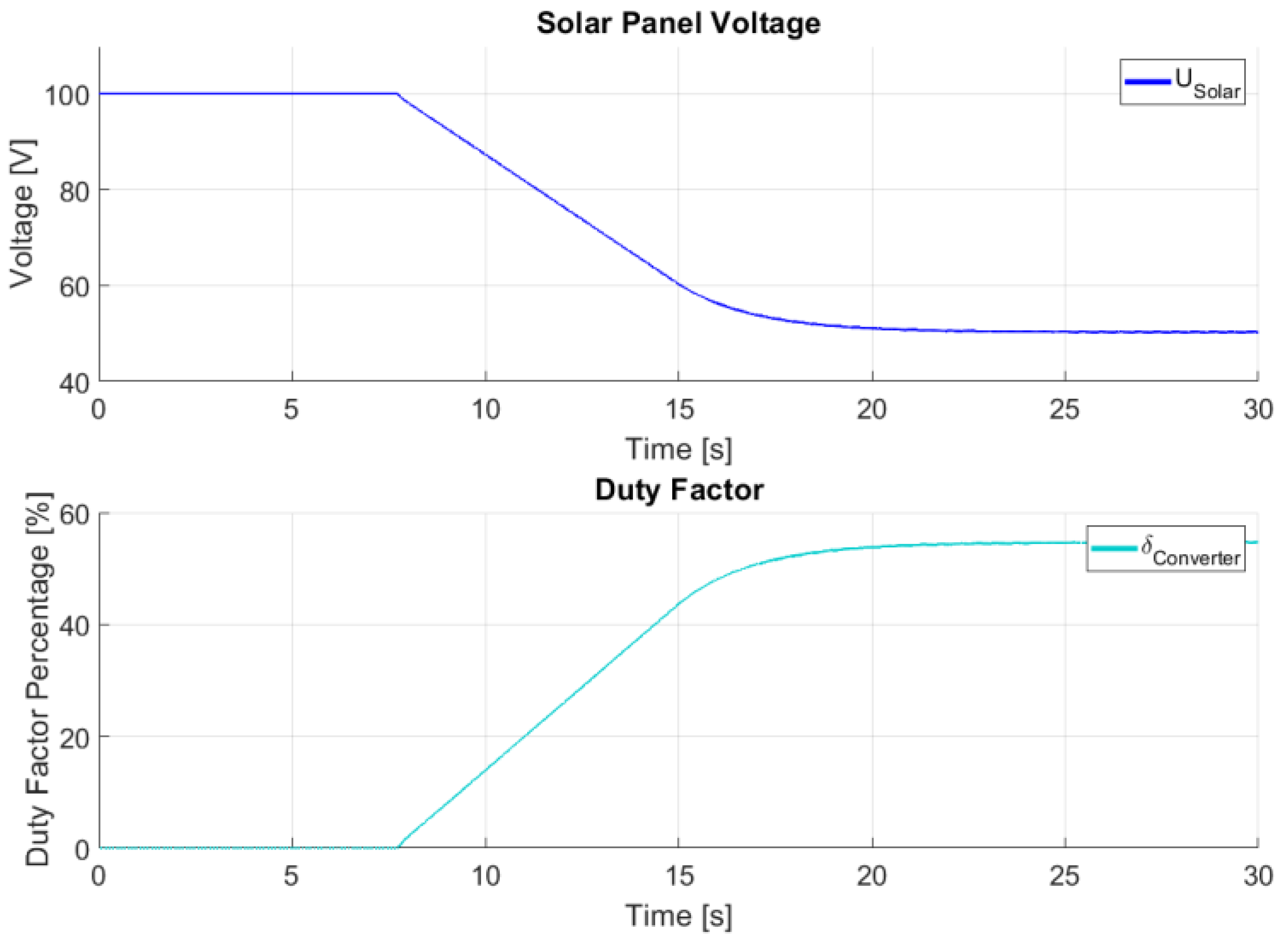
Figure 25 illustrates the validation of solar panel voltage and duty factor.
Based on the simulation results from MATLAB/Simulink MPPT implementation, the input current slowly changes at a rate defined by its maximum derivative. This allowed the associated flags to be tested for their ability to initialize the converter as well as for preventing available current wind-up, as shown in
Figure 26.
A restriction on the input current setpoint is implemented to prevent wind-up, thereby minimizing overshoot possibilities. The feedback current analytical value corresponds to the simulation, further validating this implementation.
Based on the previously theoretical and simulation results, this chapter concludes with the successful implementation and simulation of two models, namely a closed-loop solar panel regulator and a maximum power point detection circuit.
3.4. PCB Implementation
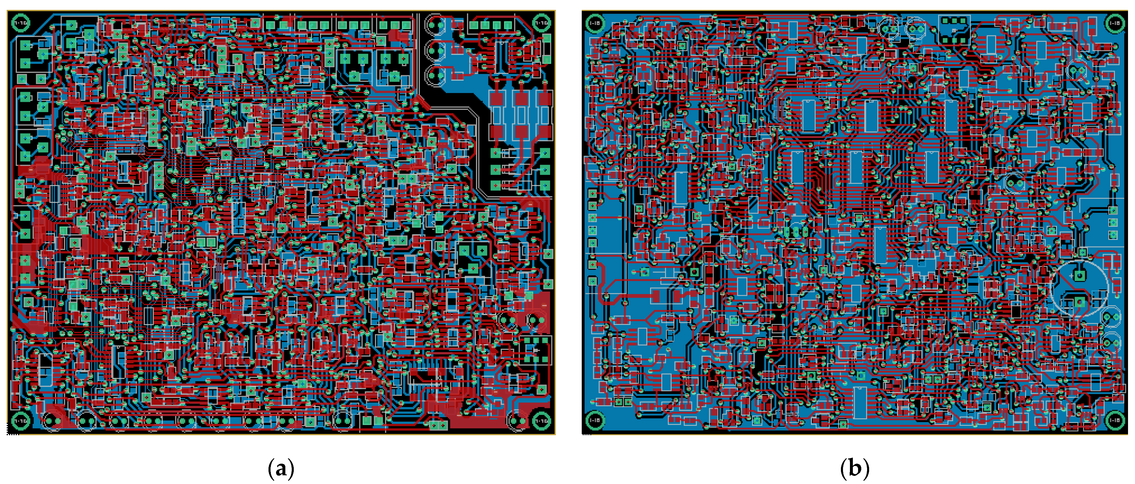
The resulting PCB implementations for both CVCC regulator and MPPT detector are illustrated below, in
Figure 27.
Both circuits were implemented using conventional PCB footprints for testing purposes, such as footprints measuring approximately 3 by 1.5 mm for resistors and capacitors as well as SO8, SO14, and other applicable footprints for additional components. The MPPT circuit acts as a mask PCB, with pins from this board providing ground connections to the CVCC circuit board using 100 mils through-hole connectors, for minimizing the overall ground trace length. Both boards presented were implemented at the approximately same size.
3.5. VLSI Estimation for ASIC Regulator Dimensions
This section estimates the resulting ASIC size for fulfilling both previously described functionalities, namely CVCC and MPPT. Several considerations were applied to the integrated circuit size calculation.
Prior to the advancements of state-of-the-art circuit integration, the minimum feature size was estimated to reach close to 100 nm [
34]. Based on the further advancements of integrated circuit manufacturing technologies, the use of EUVL (Extreme Ultraviolet Lithography) based on 13.5 nm wavelength ultraviolet light [
35], features as small as 5 nm can be manufactured, and by considering the applicability of novel innovations, features as small as one nanometer could be achieved in near future [
36].
Lithography feature size varies greatly depending on several factors [
37,
38,
39]:
Manufactured component specifications;
Applied lithography technique;
Chemical composition of wafer as well as layer and substrate substances;
Number of series or parallel sub-features required for one main feature, such as for implementing transistor gates with multiple components.
Between 1 and 1000 steps per feature were considered in this estimation, with one step involving 25 square nanometers considering the EUVL manufacturing technology. The following estimations were applied to each component from the PCB prototype:
A single feature for resistors and diodes;
A single feature for each 100 pF of capacitance;
Three features for each transistor;
One hundred features for each individual operational amplifier or analog integrated circuit;
Three hundred features for each full-package digital integrated circuit.
Based on all used components for the CVCC regulator, the estimated component minimum area at one step per feature was calculated based on the data in
Table 4, below.
Summing all lithography surface values, the estimation results in 0.9633 square micrometers, or by considering a factor of 1000 as unidimensional multiplier margin, the previous result would be expressed in square millimeters instead.
The estimation for the MPPT circuit is specified in
Table 5, for which the area was calculated based on the previously mentioned considerations, namely for one step per feature.
Having the MPPT circuit prototype lithography estimation, the minimum resulting integrated circuit surface is approximately 0.9593 square micrometers or, considering 1000 as the unidimensional multiplier margin, the same value expressed in square millimeters as maximum area.
By summing the two surface estimations, the ASIC reduction for both simulated circuits would cover a maximum area of 1.9226 square millimeters, being comparable to the MSPM0C1104 microcontroller, which measures approximately 1.4 square millimeters [
40], while potentially providing performance comparable to the presented models. However, connections to external circuits, such as resistor bridges involving high-voltage components, were excluded from this estimation.
4. Discussion
Based on the previously obtained results, tolerance associated with electric components may impact the functionality of this design. When designing all circuits, non-idealities were considered and compensated for using auxiliary circuits. Furthermore, to complete this design, the future implementation of conditioned power supplies and additional conversion circuits is necessary for this power supply unit.
The trace length was minimized, reducing the potential effects of electromagnetic interference for experimental design. Perturbations could influence the outcome of prototype operation and induce voltage spikes, triggering error codes erroneously if not filtered adequately. For this reason, the electric circuit and printed circuit boards were optimized for both the CVCC controller and the MPPT detector, thereby minimizing the occurrence of hazardous events.
Considering the estimated ASIC dimension, for a bidimensional projection of all integrated circuits and hypothetical three-dimensional manufacturing in height for the remaining or occurring tolerances, the estimated size is comparable to the smallest microcontroller, reported in March 2025, namely MSPM0C1104. Despite potentially exceeding this size, the proposed hypothetical ASIC could withstand higher perturbations in contrast to the previously experienced issues related to microcontroller shutdown due to intense perturbations, occurring from approximately 10 amperes for the regulator output current. Furthermore, internal components of microcontrollers were affected by perturbations, such as watchdog timers, leading to the previously experimentally confirmed inoperability of circuits which use embedded data memory above certain perturbation thresholds. The operability of these previous designs required the complete resetting of the system by disabling and enabling the main power supply.
This converter is assumed to operate by regulating energy from solar panels, provided by high-power lasers, into electricity, or being part of aerospace applications and converting solar power for various satellite prototypes. For this reason, the operation of this converter was associated with the operation of conventional solar panel microgrid systems.
5. Conclusions
In this study, we aimed to develop a power supply mathematical model to improve the functional, robust, and sustainable aspects of regulator circuits with applicability for BMS systems in solar energy conversion. The energy storage unit transient characteristics were improved while designing the circuits to split the converter unit, comprising both CVCC and MPPT prototypes, from most reprogrammable memories. This could result in a more reliable and sustainable solution for space-based solar power applications by mitigating issues related to electromagnetic interference, which can potentially cause the depletion of read-only memory and perturbation of random-access memory through various circuit paths. Additionally, the improvement in stability could ensure a more stable operation in perturbed environments, such as during the occurrences of gamma-ray bursts in space or various radiation types able to bypass typically used anti-perturbative protection layers.
To implement this mathematical model and electric circuit, we analyzed the feedback path stability by evaluating various criteria, such as phase margin and the presence of residual harmonics in several transfer functions. The next step involved selecting high-quality components, minimizing non-idealities such as offset voltage in operational amplifiers, leakage current in MOSFET transistors that affect power product measurements, and slew rate, which allows for communication with required digital circuits.
Furthermore, the development of an alternative inner feedback path further improved the transient performance of charging current, reducing the occurrence of current spikes in energy storage units during load variation. This result could also provide an improvement in discrete domain digital solutions used in distance energy transfer applications, considering the future compensation of interference-related issues for memory units in highly perturbed environments.
Additional considerations were analyzed during this study, including the hypothetical ASIC VLSI estimation, resulting in footprint dimensions comparable to state-of-the-art microcontroller dimensions. This result demonstrates the potential for integration processes when reduced lithography size is used to manufacture integrated components, potentially resulting in ASIC components with capabilities similar to embedded controller units. By developing this solution, considering the advantage of being split from data memory, sustainability would also be increased due to the ease of maintenance and extended service life, as it eliminates the need for compiled source code and programming units.
In conclusion, the successful improvement of transient characteristics, as well as robustness and sustainability, for a possible SBSP converter unit was achieved by developing this power supply mathematical prototype and, respectively, analyzing additional integration possibilities. Further applications of this model would include the use of an improved variant in aerospace models to obtain a comprehensive functional model for an alternative distance energy transfer infrastructure.
