1. Introduction
Modern optoelectronic technology products are changing every day. Because of the continuous optimization of optical components, substrates of various shapes are produced [
1]. In this respect, the high difficulty of processing traditional glass substrates has led to the greater use of plastic substrates. However, the application of plastic substrates faces several problems. For example, the limitations of plastic substrates themselves include low environmental tolerance, such as their easy yellowing in ultraviolet environments, bad adhesion, easy absorption of water vapor, and high coefficient of thermal expansion (CTE). These last three problems notably cause great trouble to coatings. Plastic substrates gradually replace glass substrates primarily because glass substrates are difficult to process into special-shaped surfaces. However, when these nonplanar substrates are coated to increase their optical performance, the optical performance often decreases. This is because traditional and physical vapor deposition (PVD) technologies have their directivity and can easily cause gradients on nonplanar surfaces. Such inhomogeneous thickness results in different property losses at different locations [
2]. Compared with some coating technologies, atomic layer deposition (ALD) can process many materials and can better cover special-shaped surfaces than PVD [
3,
4]. Thus, our laboratory chose this technology.
To solve the mismatch between films and plastic substrates, a paper published by K. Pfeiffer et al. in 2019 [
5] mentioned that the use of an adhesion layer or the plasma surface treatment of a substrate can effectively solve the adhesion problem of plastic substrates. Under plasma-enhanced ALD (PEALD) technology [
6], the spectral performance of films indicated that they had good uniformity, with their spectra changing little after 16 h of environment testing under ISO 9022-2 conditions [
5].
In 2017, Lae Ho Kim et al. deposited hafnium dioxide (HfO
2), aluminum oxide (Al
2O
3), and Al
2O
3/HfO
2 composite films on a P-type Si (100) substrate and soda-lime glass in a 6 in. PEALD chamber to study their water vapor permeability and chemical and physical properties [
7]. These authors found that the Al
2O
3/HfO
2 composite film could reduce water vapor penetration and even improve surface roughness. Meanwhile, regarding the CTE and film mismatch of plastic substrates, we relied on many recent studies on the yield strength, hardness, and ductility of composite materials [
8,
9,
10,
11,
12,
13]. We found that these properties decrease after crystallization. Thus, avoiding crystallization and adjusting various aspects of these properties is a major study direction.
In 2020, Kim et al. used ALD to deposit HfO
2 single-layer films using different processes. At the same process temperature of 250 °C, the intensity of XRD and film roughness of PEALD were higher than those of thermal ALD (THALD) [
14]. In 2017, Yaowei Wei et al. found that when HfO
2 was deposited using ALD at 250 °C, the refractive index and intensity of XRD increased as the number of cycles increased [
15], and the HfO
2 film began to crystallize at 500 cycles. However, plastic substrates do not tolerate high temperatures, so THALD is obviously not a suitable technology. Thus, controlling the PEALD deposition film without crystallization is a key point of study.
In 2017, Svetlana Shestavea et al. discussed film stress using PEALD to deposit HfO
2, silicon dioxide (SiO
2), and Al
2O
3 [
16]. They found that inserting multiple 3 nm and 1.5 nm Al
2O
3 layers in a 200 nm thick HfO
2 film could effectively reduce film stress. In addition, they observed that there was no cavity between the HfO
2/Al
2O
3 composite layer and the substrate and that good adhesion was maintained. When they used HfO
2, the temperature, stress, and surface roughness were lower, indirectly proving that the possibility of crystallization was lower.
Because the combination of HfO2 and Al2O3 layers can improve their surface roughness and reduce stress, these two materials were chosen in this study. In addition, considering its optical properties after making a multilayer film, SiO2, which has the lowest refractive index among various oxides and has small dispersion and absorption, was selected as the third design material. According to the above discussion, the clever use of insertion layers between the selected materials to avoid crystallization is the key point of this research.
2. Materials and Methods
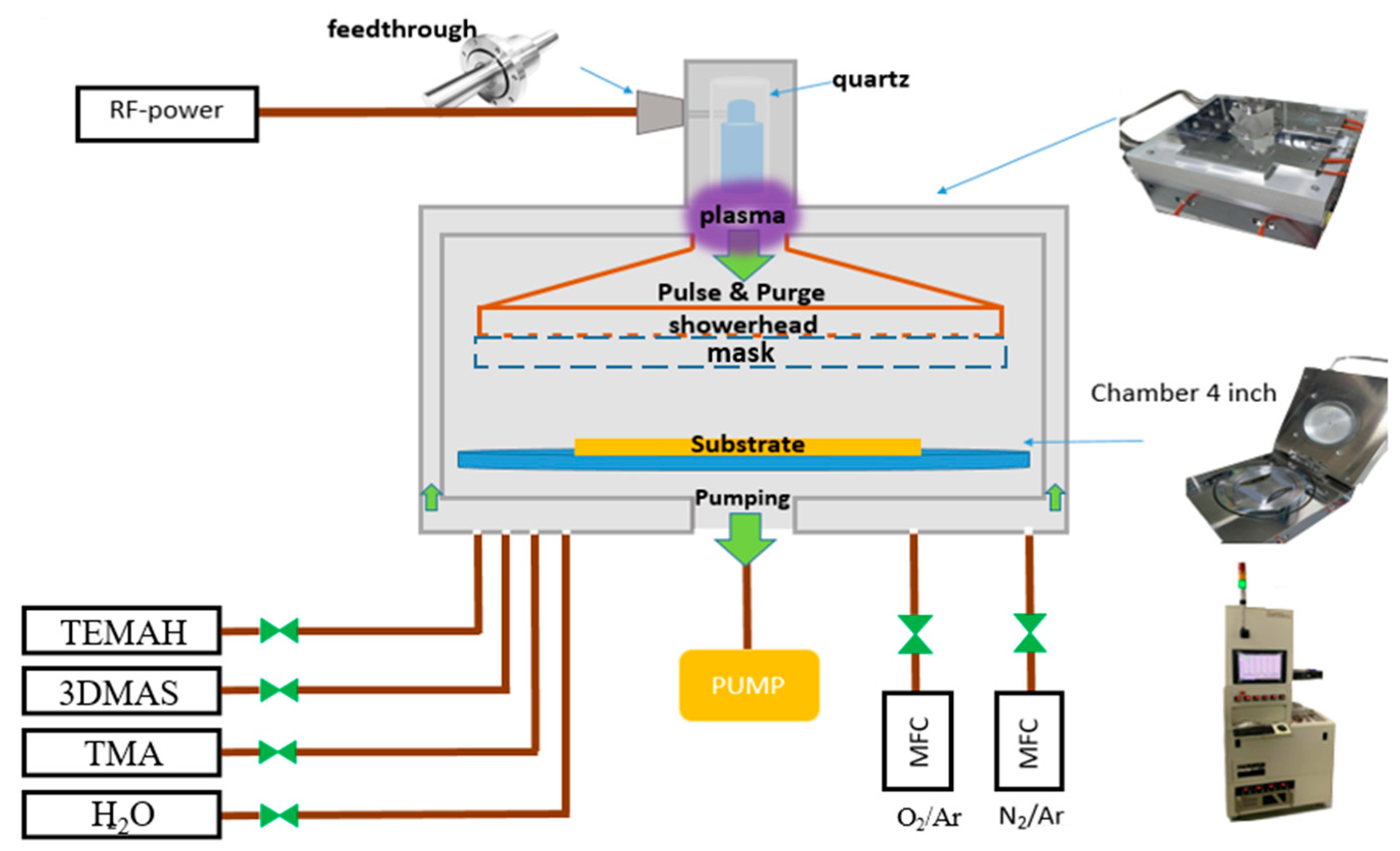
The process utilized for the coating process in this experiment was PEALD. It utilized a mechanical pump, and the deposition process started after the vacuum pressure reached 10 mTorr. The precursors of Al
2O
3, SiO
2, and HfO
2 are trimethylaluminium (TMA), tris (dimethylamino)silane (3DMAS), and tetrakis (ethylmethylamino)hafnium (TEMAH), respectively. The equipment was equipped with three heating devices: a precursor, a pipeline, and a chamber. The precursor was heated using a heating cloth that covered the bottle body, whereas the pipeline used a heating tape to prevent steam condensation due to low temperatures, which could result in decreased flow into the chamber. Meanwhile, the chamber was heated using an electric resistance wire. All three heating methods were monitored using thermocouples. The plasma source was based on remote radio frequency technology [
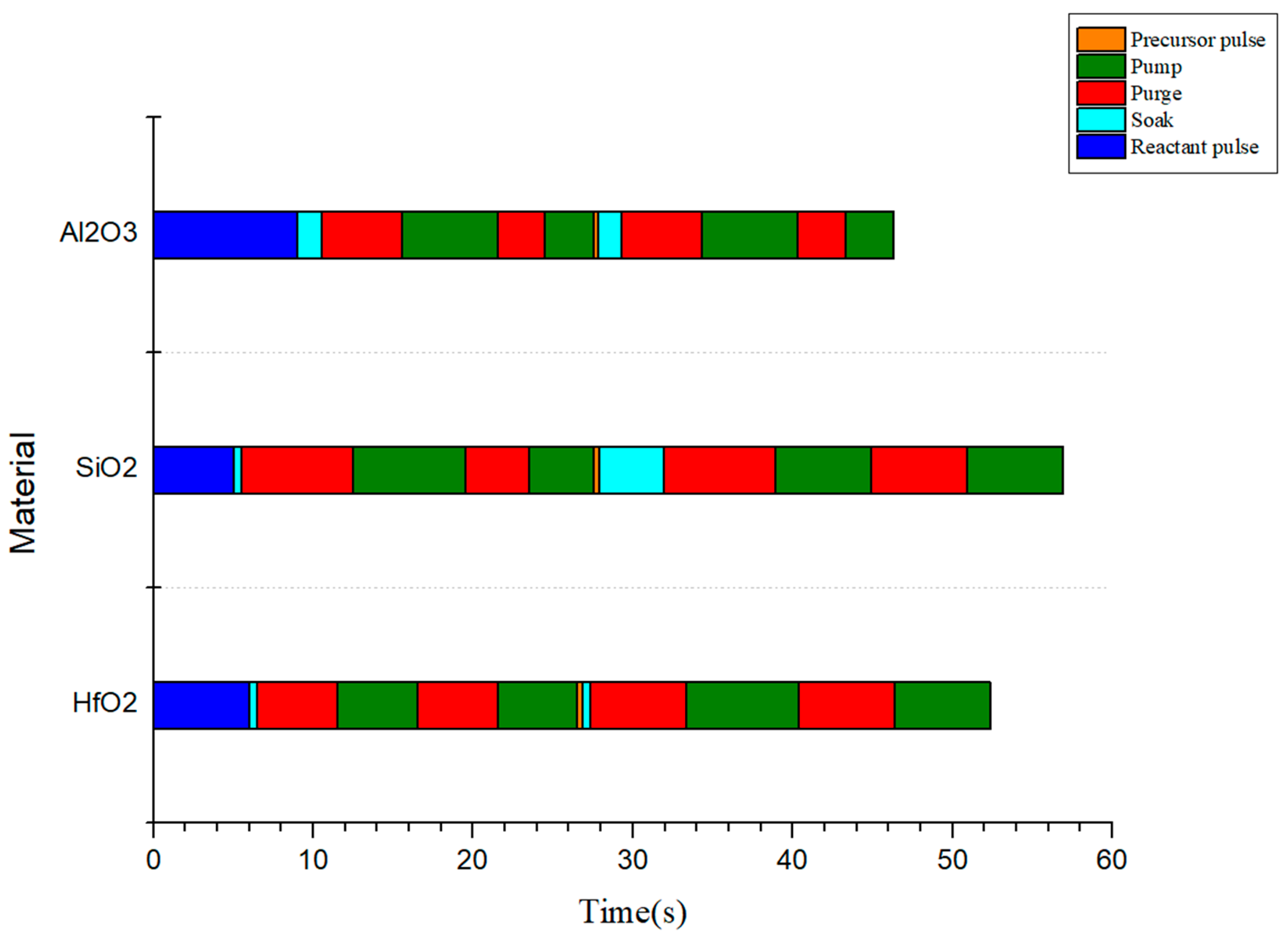
17] and was introduced into a quartz-coated electrode column via a feedthrough to enhance plasma effectiveness. Finally, the coating was evenly spread onto the substrate through a showerhead. The system architecture and coating process parameters are illustrated in
Figure 1 and
Figure 2, respectively.
The following instruments were utilized for measurement and validation in our experiments. Thin films with a predetermined thickness were deposited using coating equipment. Then, an ellipsometer (SENTECH’s SENresearch 4.0) was used to fit the thin film thickness, refractive index, and extinction coefficient. Furthermore, X-ray diffraction (XRD; Bruker D8 ADVANCE XRD instrument) was used to analyze the film crystallization and was used with a Veeco Innova Atomic force microscope (AFM) produced by Bruker to examine the film roughness. Using various data feedback obtained by the ellipsometer, XRD, and AFM, we reviewed and adjusted the film process parameters to achieve optimal film settings. After coating multilayer films with different film thickness designs, the samples were measured using a HITACHI UH4150 spectrometer for transmittance and reflectance to compare with the original simulated data, and the true film pile-up was observed using a transmission electron microscope (TEM; JEOL, JEM2100) which produced by JEOL. Finally, the finished product was put into a programmable constant temperature and humidity machine (GTH-080ST-SP; Jufu Instruments). According to the EIAJ ED-4701/100 standard, the environment tolerance of the sample was observed at a humidity of 85% and a temperature of 85 °C, and a 10× Zeiss Axioskop duplex optical microscope (OM) was used to observe microscopic appearance changes.
3. Results
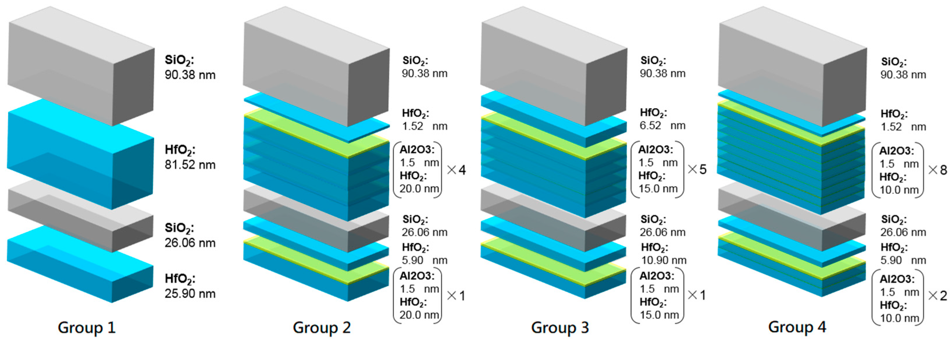
Four layers of AR films were coated on a poly(methyl methacrylate) (PMMA) substrate, and the experimental design was assigned into four groups. The thickness of SiO
2 in the four groups was not changed, but there were different HfO
2/Al
2O
3 ratios to make nanolaminate. Group 1 was the original design without any layers inserted. Group 2 had a 1.5 nm thick Al
2O
3 layer inserted for every 20 nm of HfO
2, and there were four pairs in the nanolaminate. Group 3 had a 1.5 nm thick Al
2O
3 layer inserted for every 15 nm of the HfO
2 layer, and there were five pairs in the nanolaminate. Group 4 had a1.5 nm thick Al
2O
3 layer inserted for every 10 nm of the HfO
2 layer, and there were eight pairs in the nanolaminates. The design diagram is shown in
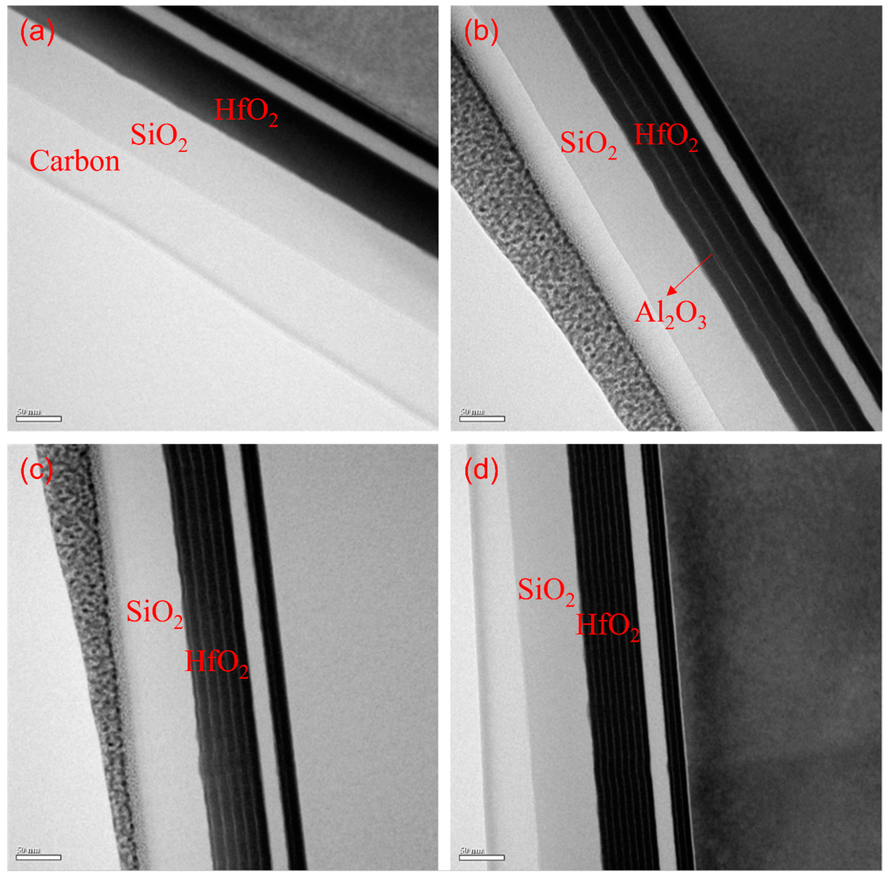
Figure 3. Meanwhile,
Figure 4 shows the actual stack conditions of the design groups corresponding to TEM. In the following, we propose five key factors to discuss the optical properties and environmental test results produced by different designs.
3.1. Material of Thin Film
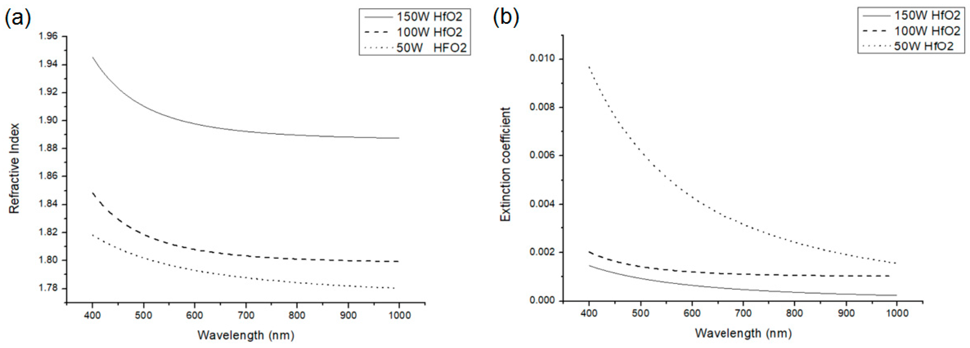
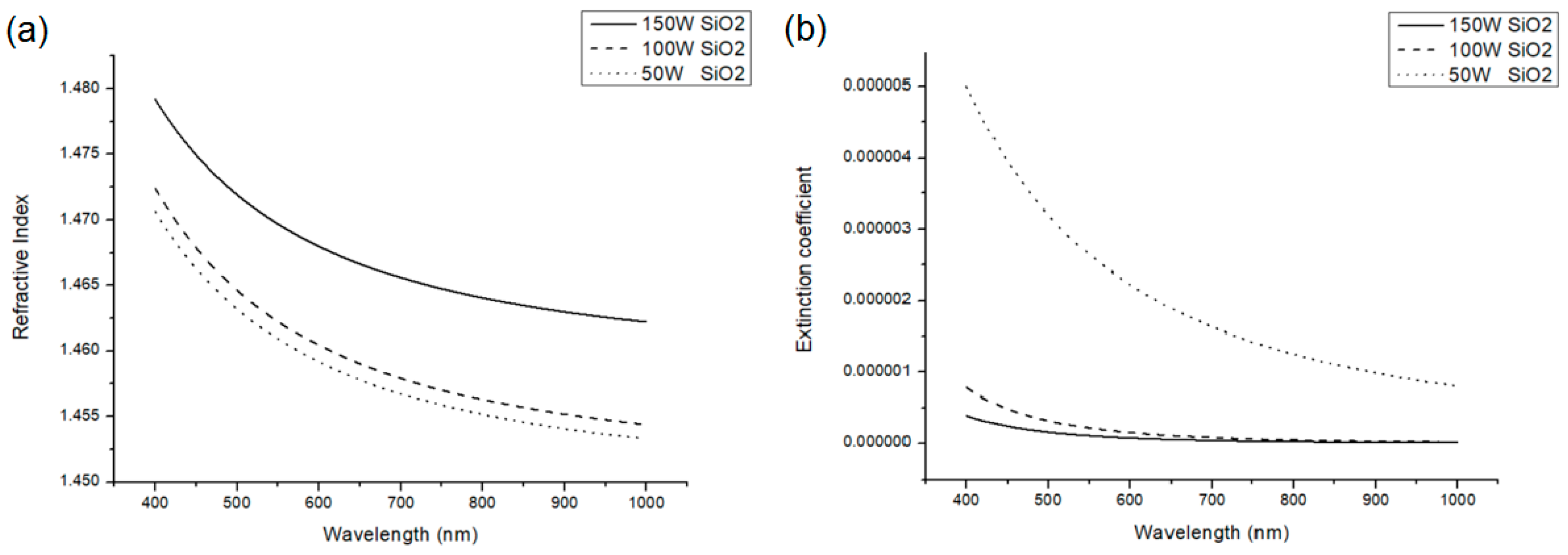
In terms of the optical properties of the three materials, we achieved good n values and low k values. As mentioned in the literature, the higher the packing density, the greater the refractive index [
18].
Figure 5 and
Figure 6 show the refractive index and extinction coefficient of HfO
2 and SiO
2. The n and k values were measured using an ellipsometer. Indeed, at 150 W, the refractive index was the highest and the extinction coefficient was the smallest.
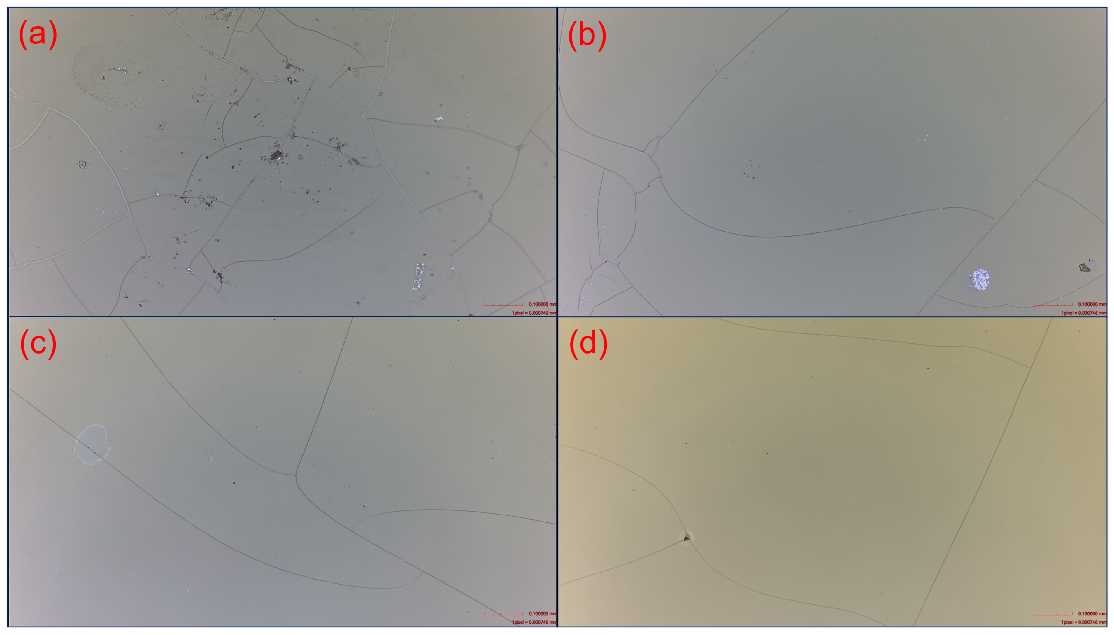
Although the plasma power of 150 W produced the maximum refractive index and minimum extinction coefficient, it caused film cracks on the plastic substrates (
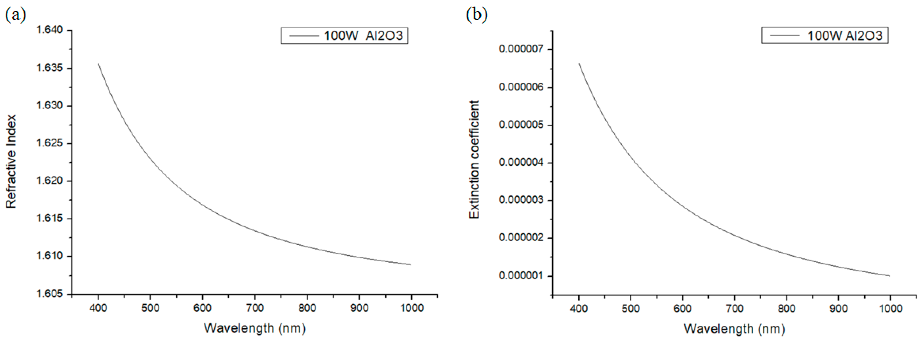
Figure 7). To prevent the absorption from being too much and to avoid causing film cracks, we chose to reduce the plasma power to 100 W and used this power to form an Al
2O
3 film. The obtained refractive index and extinction coefficient are shown in
Figure 8. The data on the refractive indices and extinction coefficients of HfO
2, SiO
2, and Al
2O
3 are summarized and listed in
Table 1.
3.2. Surface Roughness and Intensity of XRD
To ensure the completeness and effectiveness of the oxidation reaction during the experiment, plasma was used to produce the oxidation reaction, and Ar was added to the plasma to improve the efficiency of the oxidation reaction [
19]. According to different thicknesses, this experiment found a positive correlation between surface roughness and intensity of XRD. The experimental data are shown in
Table 2.
There were different intensities of XRD under different cycle numbers, as shown in
Figure 9. When the cycle was at 700, the intensity of XRD was the highest, reaching 2256.09. The surface roughness under different cycle numbers is shown in
Figure 10. When the cycle was at 700, the surface roughness also reached 1.25 nm. As the cycle number dropped to 300, the intensity of XRD was only about 1/7 of the origin, and the surface roughness was less than half of what it was at a cycle number of 700. At this time, inserting the Al
2O
3 could significantly reduce the intensity of XRD. The data obtained are shown in
Table 3.
3.3. Nanolaminates
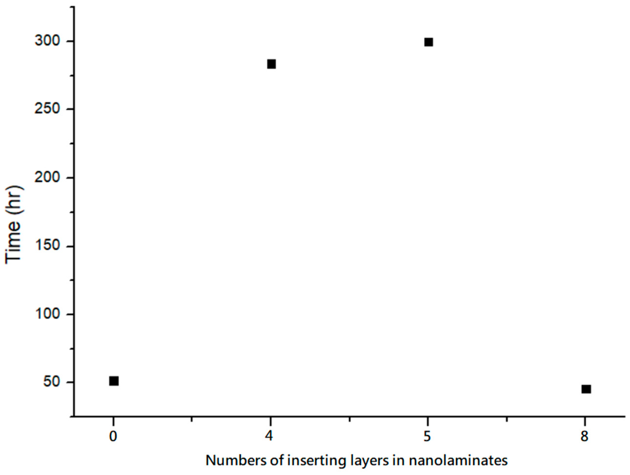
Figure 11 shows the surface of different numbers of inserted layers in the experiment observed using an OM, and the cracking state began to appear after different environmental test hours. The original design without inserted layers cracked after 52 h, which was observed using an OM. Meanwhile, the environmental test time grew and even reached 300 h when five layers were inserted. When eight layers were inserted, the environmental test time reached the lowest of 46 h, which was even worse than that of the unprocessed design.
In this experiment, the PMMA substrate was coated with multilayer films, including one with no inserted layer and those with four, five, and eight layers inserted.
Figure 12 shows that the best environmental test time was achieved when five layers of Al
2O
3 were inserted. Under this design, environmental tests verified the Al
2O
3 thicknesses of 1, 1.5, and 2 nm (
Figure 13).
According to the environmental test data, if 1 nm Al
2O
3 insertion layers were used, the environmental testing time increased significantly from 300 to 352 h when using 1.5 nm. In other words, as the insertion layers’ thickness decreased, the environmental test results became better.
Figure 14 shows the cracking status of different Al
2O
3 layer thicknesses after different hours of environmental tests. At the same scale, cracking under 2 nm Al
2O
3 insertion layers had more intertwined fine lines. As the thickness of the insertion layers decreased, the density of these fine lines gradually became smaller.
3.4. Optical Properties
The AR coating was deposited on the PMMA substrate using the four previous designs with HfO
2, SiO
2, and Al
2O
3, and the corresponding spectra were measured as
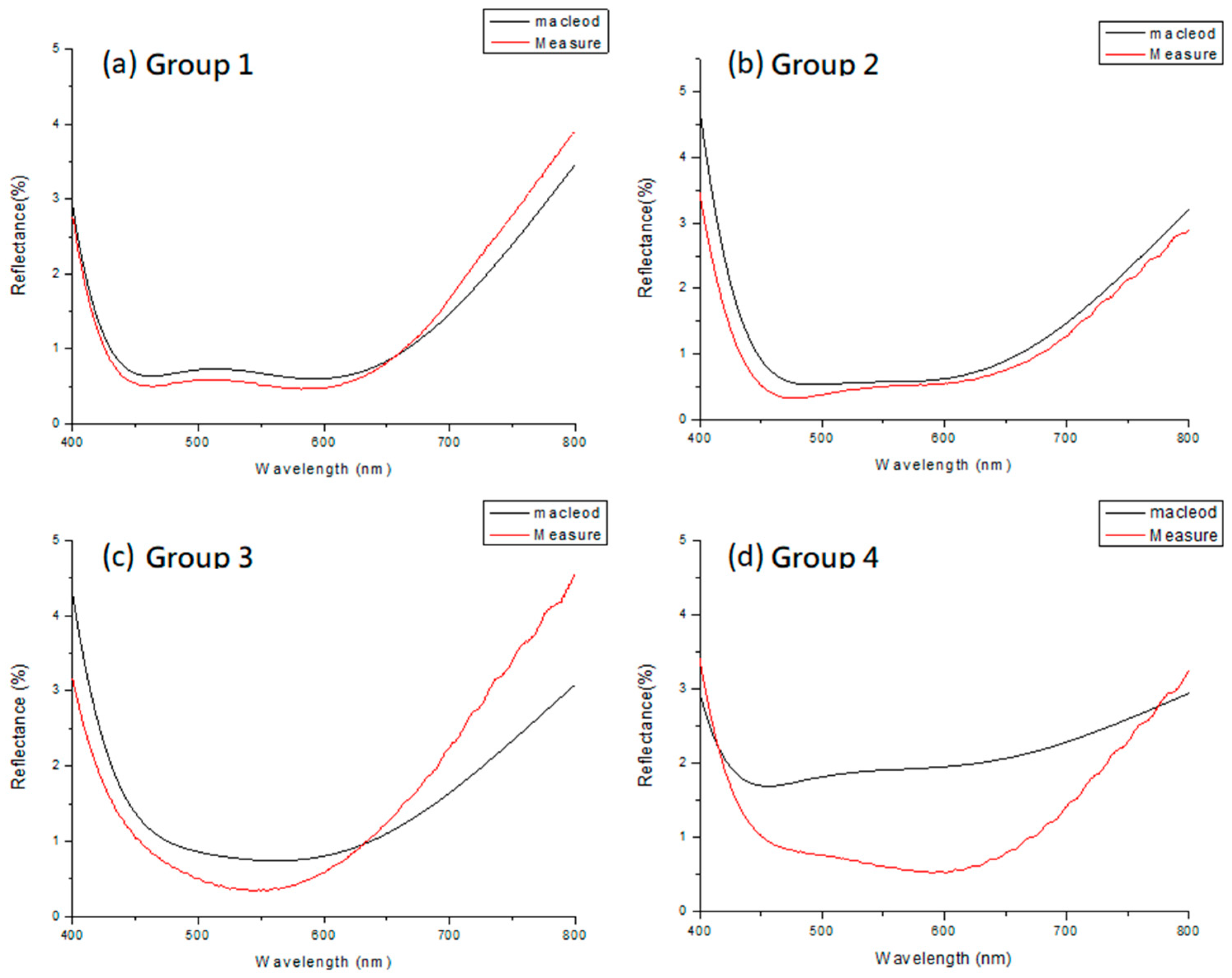
Figure 15 shows. The original design without inserted layers had a measured spectrum similar to the design spectrum, with an average reflectance of about 0.67%. If the five layers of Group 3 were used (
Figure 16), even if the Al
2O
3 layer’s thickness was changed to 1 and 2 nm, the difference in the center wavelength of the spectrum was not significant.
4. Discussion
First, in this study, as shown in
Section 3.1, we increased the refractive index by increasing the temperature and increasing the plasma power. Increasing the temperature and plasma power provided enough migration energy between molecules to increase the packing density and help complete the reaction to reduce the K value. However, the high deformation and easy deterioration of plastic substrates must be considered, and this cannot be achieved by increasing the temperature and plasma power as in the past. For plastic substrates, we must lower the process temperature to 60 °C.
Second, according to the references above, the issues related to the interfaces of composite materials can be classified into three categories: strength, hardness, and ductility. The mechanisms regarding strength and hardness are included in three scale ranges. The first is the Hall–Petch scale, which is related to the strengthening and hardening of nanocomposite layers and dislocation pile-up on interfaces [
20]. Strengthening effects operate in composite layers with relatively thick single-layer thicknesses, with the strength and hardness increasing as the thickness decreases on the scale of hundreds of nanometers. The second scale is at tens of nanometers, and the strengthening and hardening mechanism is a confined layer slip. At this scale, as the thickness decreases, the strength and hardness increase slowly because a single dislocation ring is in the layer. If the distance between layers is insufficient, the dislocation rings also decrease, so it is more localized to the thickness of a single layer [
21,
22]. The last scale is the interface barrier strength (IBS), which is related to the passage of a single dislocation through the composite interface, and the thickness is only a few nanometers [
23].
In Hall–Petch’s model, reducing the grain size increased the strength of the material. This experiment believed that grain size was related to surface roughness. In the study by Lae Ho Kim et al. (2017), the addition of Al
2O
3 insertion layers reduced the surface roughness of HfO
2 [
7]. That is why we reduce the film thickness in
Section 3.2 and find the correlation between surface roughness and intensity of XRD.
Third, when using the insertion layers, the above experiments showed that the cycle positively correlated with the surface roughness and intensity of XRD. Therefore, when the thickness of HfO
2 decreases, the intensity of XRD and surface roughness are expected to decrease. Meanwhile, Svetlana Shestavea et al. used ultrathin Al
2O
3 layers to reduce the thickness of HfO
2 and improved the stress from 660 to 440 MPa [
16]. As one of the causes of film cracks is the mismatch in the CTE between the substrate and the film, reducing stress is one way to solve film cracks. In other words, reducing the thickness of HfO
2 is expected to reduce stress, improve the mismatch between the film and the substrate, and prevent the film from cracking. When the thickness of a single layer of HfO
2 was reduced in this study, the environmental test results were consistent with those above.
The results after inserting eight layers were not logically consistent; the reason was related to a ductility issue.
Zhang et al. studied the relevance of single-layer thickness (h) on the deformation behavior of Cu/Nb and Cu/Zr multilayer films [
24]. Their results showed that the ductile behaviors of Cu/Nb and Cu/Zr multilayer films were different from those of single Nb and Zr films. The ductility arrival peaked at a specific thickness and then generally decreased as the thickness decreased, a phenomenon that was exactly the opposite of those of strength and hardness. Regarding the experimental results, the ductility of the nanocomposite layer might reach its maximum peak when the thickness of HfO
2 was 15 nm. If the thickness was thinner than 15 nm, the thickness of HfO
2 decreased, and the ductility decreased greatly. This was the reason for the film cracking in the environmental tests.
Theoretically, when the thickness of the insertion layer is in the IBS scale, the strength and ductility drop sharply. This method can localize the stress in insertion layers or resist the stress to suppress fractures, that is, when the fracture is localized in the insertion layers, the fracture is not extended [
24]. As the thickness of the insertion layers increases, the number of environmental test hours decreases because the ductility increases when the thickness of the insertion layers increases at this scale. When the ductility increases, the stress is not localized or interrupted in the insertion layers, so there is a greater chance for the energy to penetrate, leading to comprehensive membrane cracks.
Finally, we considered the role of optical properties. The measured spectrum of Group 2 began to slowly deviate from the simulated spectrum of the original design, with the degree of deviation being greater than that of Group 1. Similarly, the degree of deviation of Group 3 was greater than that of Group 2, and that of Group 4 was greater than that of Group 3 (
Figure 15). The greater the number of inserted layers in nanolaminates, the more serious the degree of deviation from the simulated spectrum [
18,
25].
As the number of inserted layers increased, the difference between the real spectrum and the simulated spectrum became larger. However, when we inserted five layers in the nanolaminates, the change in reflectance of the spectrum was still acceptable. If the five-layer design was used and Al2O3 was adjusted from 1.5 to 1 and 2 nm thick, respectively, the difference in the spectral center wavelength on the PMMA substrate was small. Considering the significant improvement in the environmental test tolerance properties, compared with the variation in spectral performance, this can be ignored in actual applications.
