1. Introduction
The continuous and effective use of renewable energy sources is one of the key activities that can be used to minimize carbon dioxide emissions deriving from the energy conversion process. Governments, industries, and general consumers have a growing interest in solar energy, mainly photovoltaic (PV) [
1]. From the point of view of enabling technologies, several challenging issues must be tackled to achieve high performance and further increase the penetration of renewable power options. One of these challenges is to efficiently increment the low voltage output of solar panel blocks to the required voltage levels of DC loads/buses [
2].
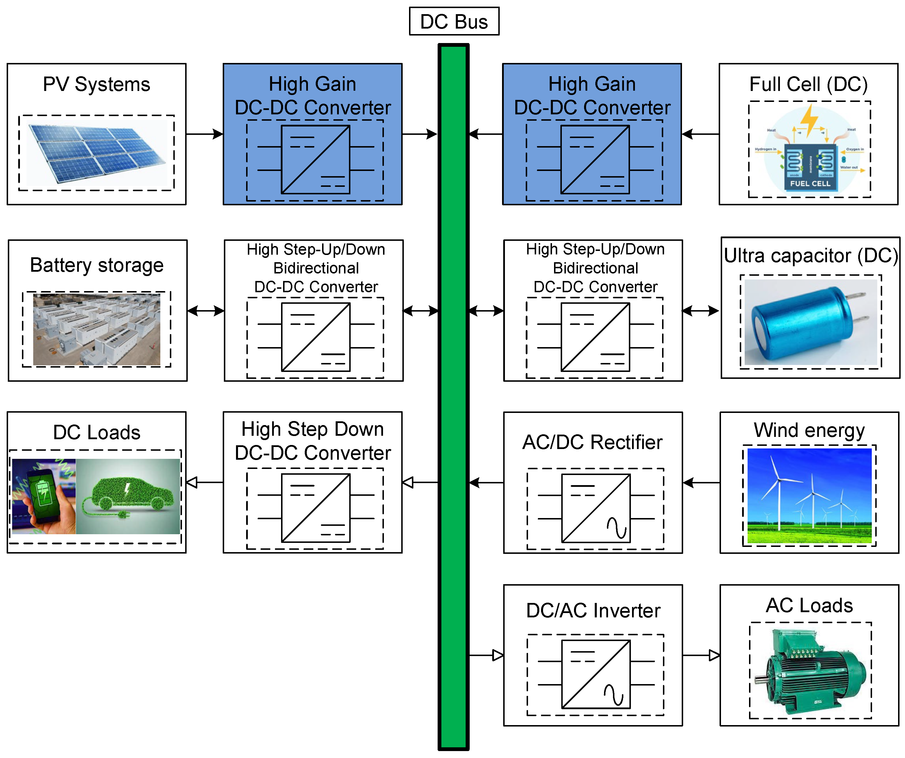
PV systems are becoming an essential type of DC microgrid, and they can have a great impact on mitigating energy poverty in rural and geographically remote locations [
3]. The interconnection voltage level of PV systems connected to a DC microgrid, more specifically to a DC bus, is around 380 V [
4,
5,
6,
7]. To reach this voltage level, the voltage output of a single panel, or a small group of panels, must be low (20 V to 60 V for a single panel) [
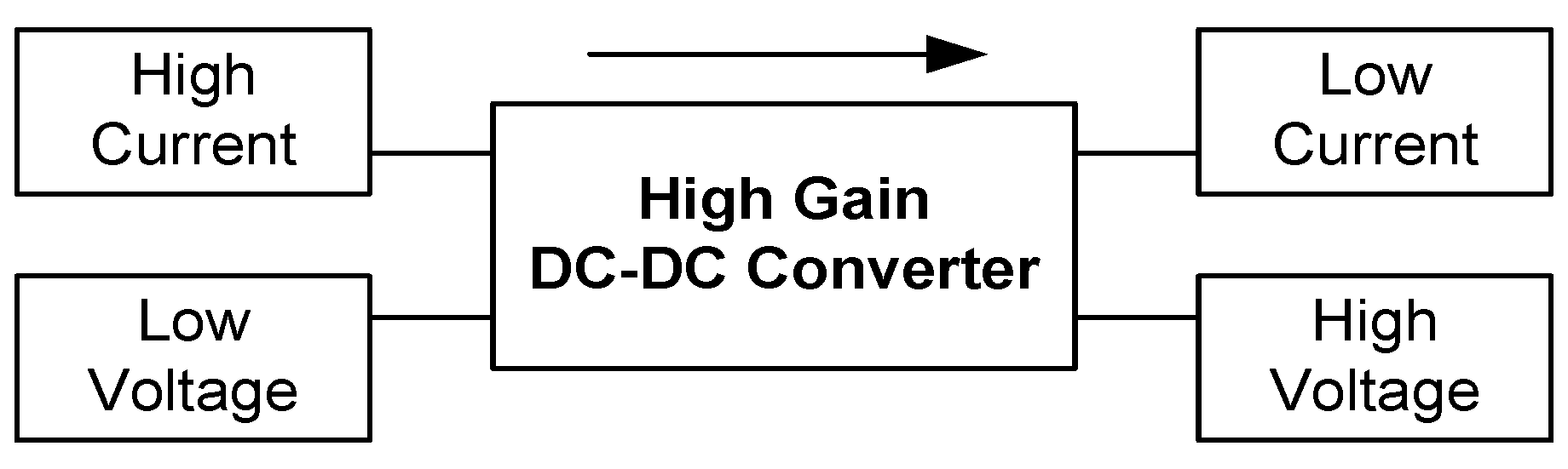
8]. Therefore, this output voltage must be stepped up, which opens the door to the development of high-gain DC-DC interfaces, as shown in
Figure 1, while keeping efficiency and performance high [
4,
5,
6,
7,
8,
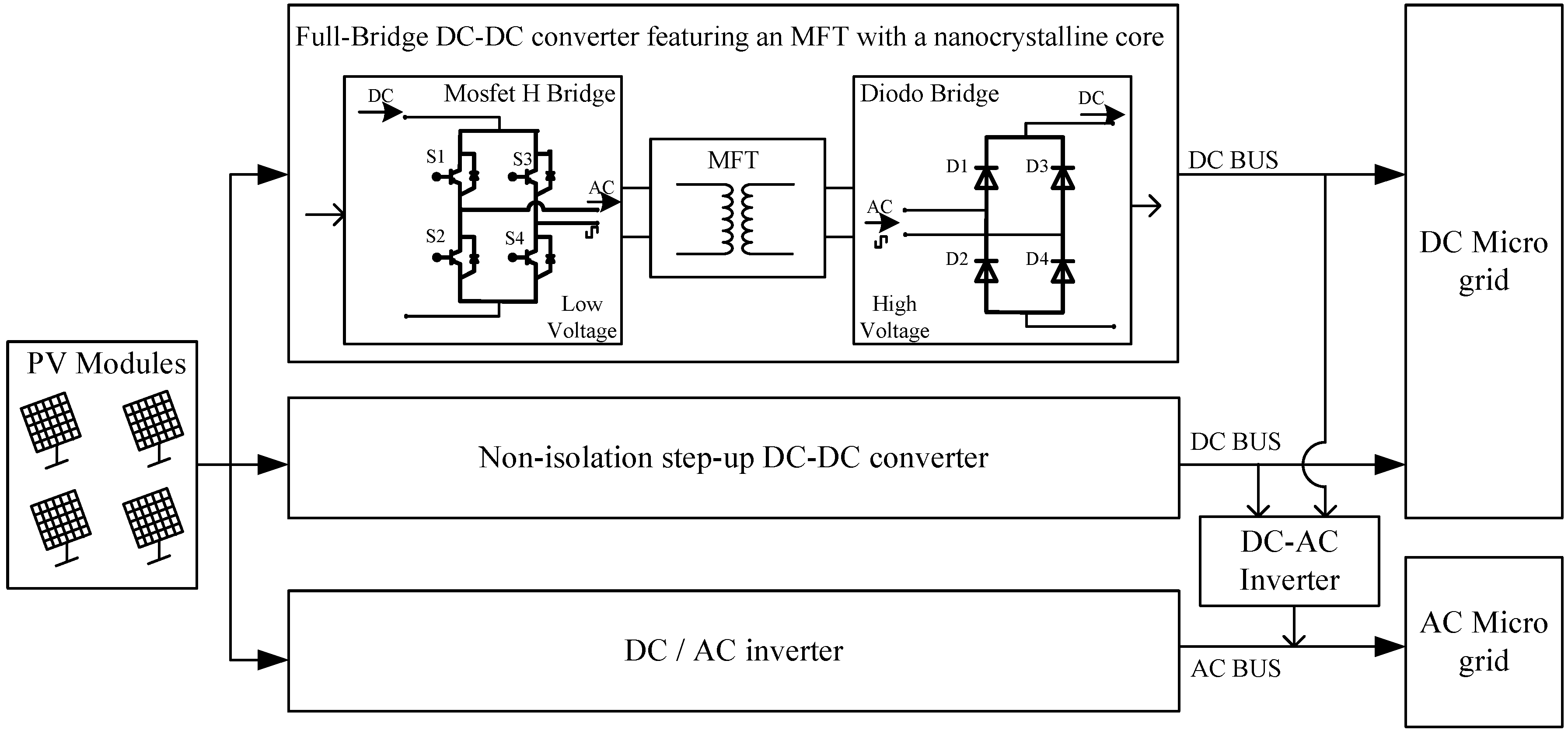
9]. Converters interconnecting photovoltaic panels and DC and AC microgrids are shown in
Figure 2. Finally, in the last few years, we have observed the development of both conventional converters [
9] as well as restructured ones [
4,
5] with the aim of stepping up the solar panels’ voltage output [
4,
5,
6,
7].
The design of converters with a high step-up voltage ratio conversion for PV applications faces issues such as a high input current and the technique for increasing voltage. If this input current is handled only with electronic commutation devices, as shown in
Figure 3, efficiency is jeopardized because of the greater losses and cost. Taking this into account, in recent years, there has been increasing interest in developing both isolated [
5,
9] and non-isolated DC-DC converters [
4,
6,
7].
The configuration of non-isolated converters lacks medium- or high-frequency transformers to step up or step down the voltage at its input [
4,
6,
7]. In this case, transformer issues, such as core saturation or efficiency, are put aside. Although this apparent advantage may benefit non-isolated converters, the lack of galvanic isolation between the solar panels and the DC buses is regarded as a drawback. In [
4], two transformerless DC-DC configurations are presented. Both configurations follow the structure of conventional boost and buck–boost converters. As expected, the voltage conversion ratio obtained is lower than 10, 1 to 8.4 (45 V/380 V), and the efficiency is 94.86%, both verified with a 110 W lab prototype. In this case, a higher voltage conversion ratio results in lower efficiency due to the increase in the current at the input.
From a similar point of view, in [
7], a DC-DC boost converter with 1 to 11.5 ratio (34 V/380 V) is presented. The results obtained with a 200 W lab prototype validate the ratio and demonstrate 93% efficiency. Also, in [
6], a DC-DC converter with a voltage conversion ratio of 1 to 15.83 (24 V/380 V) is presented. Like in other proposals, the results were validated by using a lab prototype but, in this case, specified at 225 W and 91.6% efficiency. As can be noted in previous works, the higher the step-up ratio, the lower the efficiency. Therefore, the challenge is to attain a converter configuration that has a high step-up ratio and high efficiency at the same time.
On the other hand, an isolated converter includes a medium- or high-frequency transformer. The characteristics required for such a transformer are high efficiency, low core losses, low winding losses, high power density, low working temperature, and non-saturated transformer operation [
5,
9]. Achieving all these characteristics together is a design challenge. In this work, an MFT, designed with a new approach, was used as part of the DC-DC converter structure.
With regard to isolated converters, a DC-DC half-bridge boost converter with a voltage conversion ratio of 1 to 10 (40 V/400 V) and a 94.5% efficiency is presented in [
5]. These results were validated with a 300 W lab prototype. A high step-down DC-DC converter with a 1 to 23 voltage conversion ratio and 92% efficiency is presented in another approach [
9]. These results are corroborated using a lab prototype specified at 110 W.
Some of the previous proposed converters attain efficiencies close to 95% but at the cost of obtaining a low voltage conversion ratio of 1 to 10. On the other hand, the efficiency of those proposed converters achieving a voltage conversion ratio ≥15 is lower than 92%. In these types of converters, the step-up ratio vs. efficiency relationship is inadequate for today’s PV applications.
In this context, the research problem is to determine whether DC-DC converters can be designed as an enabling technology of photovoltaic systems exhibiting a voltage conversion ratio ≥15 while keeping efficiency ≥95%. A positive solution to this challenge may result in achieving advanced converters that can further improve the performance of photovoltaic systems installations. Improved enabling technology can be one of the major players in boosting the penetration of PV systems into power grids.
Full-bridge DC-DC converters featuring new nanocrystalline-core medium-frequency transformers not only achieve high efficiency but also a high voltage conversion ratio useful to both photovoltaic systems and DC microgrids. In this regard, this paper proposes the design, simulation, and construction of a lab DC-DC full-bridge prototype featuring a medium-frequency transformer with a nanocrystalline core. The result is an advanced structure achieving a high voltage conversion ratio, 16, along with efficiency ≥95%.
Section 1 presents the state of the art of the boost converters applied to PV systems presented as well as the impact of the results of such works.
Section 2 details the structure and stages of the boost converter proposed in this paper as well as the calculation of the losses in the semiconductor devices, both in the rectifier and in the inverter. The performance of the boost converter was evaluated using the MATLAB-Simulink platform, as described in
Section 3.
Section 4 presents the experimental validation of the proposed boost converter. Finally, in
Section 5, all results are discussed and compared with those of other proposed boost converters available in the contemporary literature, while conclusions are expressed in
Section 6.
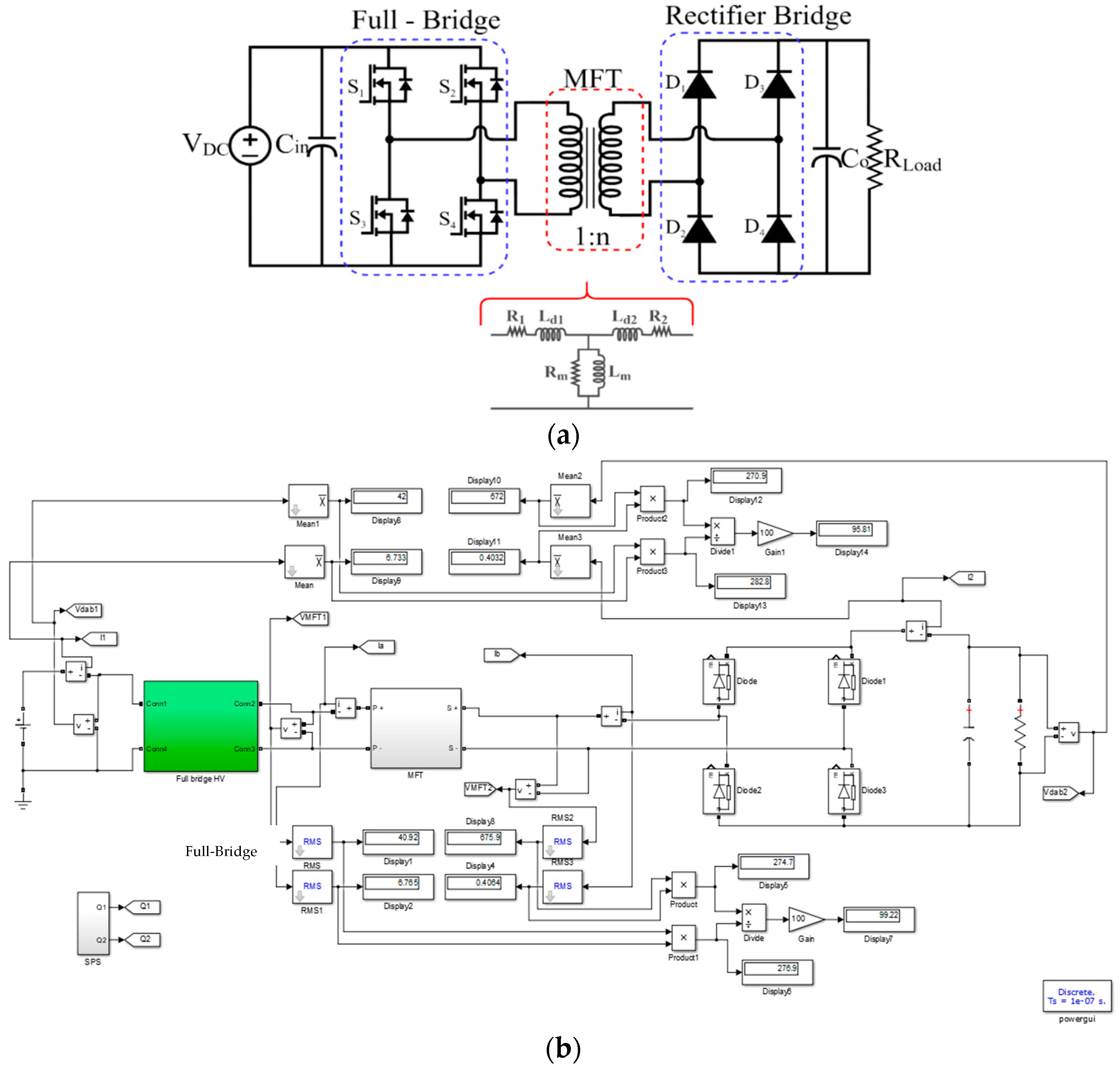
2. DC-DC Converter Structure
The specialized literature reports several proposed isolated and non-isolated converters designed for high efficiency and a high voltage conversion ratio useful for PV system applications [
4,
5,
6,
7,
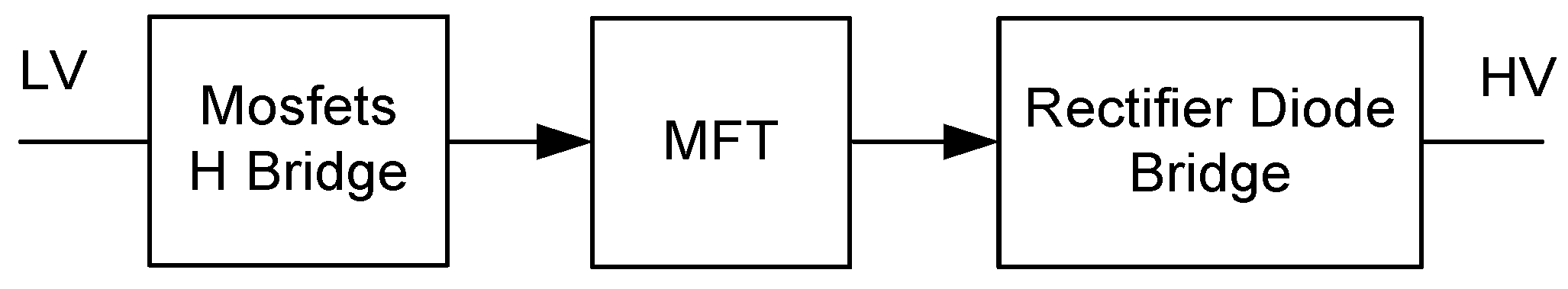
9]. Although the full-bridge configuration is a well-known structure, adding cutting edge MFTs featuring nanocrystalline cores into these designs can improve efficiency while achieving high voltage conversion ratios. The three main stages of the full-bridge DC-DC configuration featuring a nanocrystalline-core MFT are the MOSFET H-bridge, the MFT, and the diode bridge, as shown in
Figure 4. Besides the insolation provided, the MFT also increases the transformer turns ratio (transformation relation). The ratio results in an increase in the output voltage level while keeping a low level of core losses and winding losses.
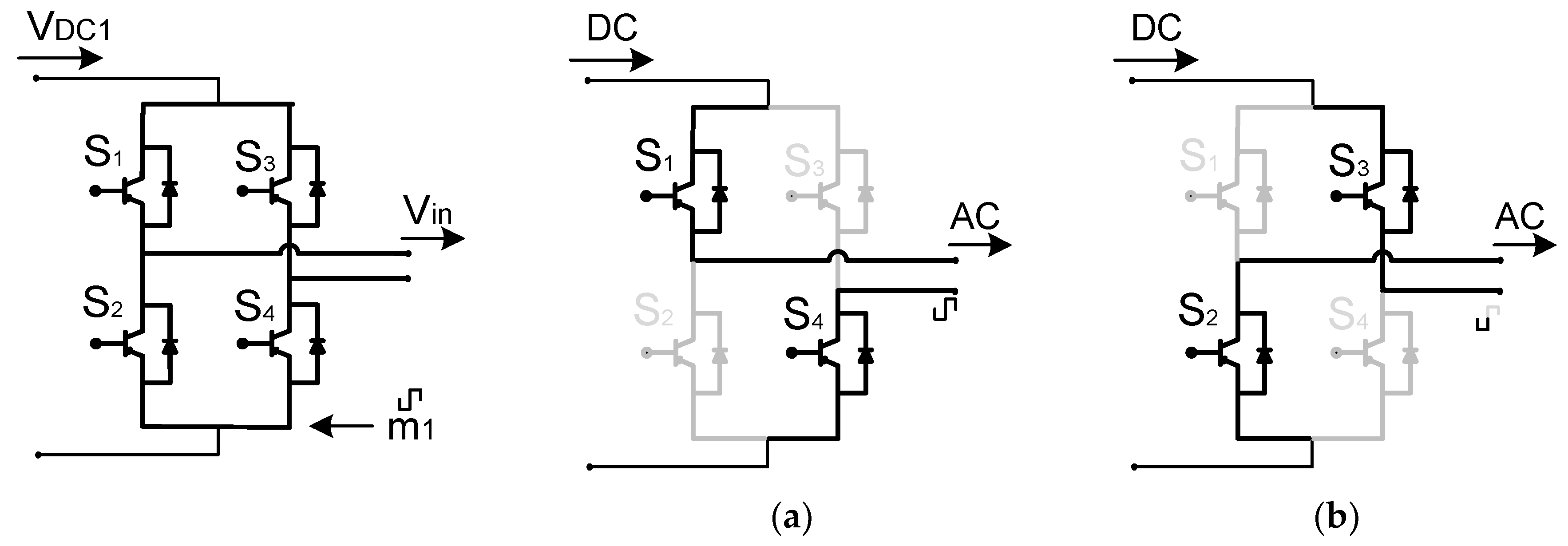
2.1. MOSFET H-Bridge
The H-bridge stage (see
Figure 5) converts the DC power signal into an AC square power signal to feed the MFT.
VDC1 denotes the DC input voltage to the H-bridge, and
Vin is the AC square wave voltage output of the above-mentioned bridge. Observe that
Vin depends on the modulation signal
m1 as shown in
Figure 5.
The H-bridge configurations found in electronic converters are generally used for either signal inversion or adding two-way signaling to DC-DC dual-active bridge converters [
10], electric vehicles [
11], and electronic transformers [
12,
13]. It is worth mentioning that the H-bridge configuration facilitates the replication of the results presented in this paper by other potential interested parties.
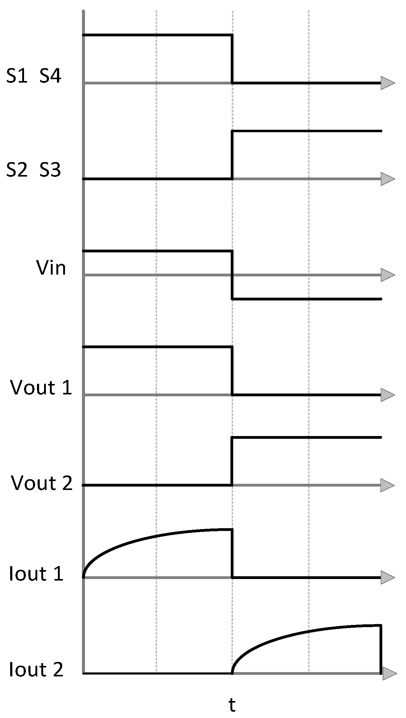
Figure 6 shows the modulation signals to the converter for the two-level voltage at the MFT. The signal to S1 and S4 is 180° out of phase from the main signal applied to S2 and S3. The control scheme is not complex, which turns into an advantage due to the ease of reproducing the results compared to other types of control techniques applied, such as robust control, which may lead to even more confusion if multilevel topologies are in use.
Losses in semiconductor devices (MOSFETs) are determined through Equations (1)–(4), where the conduction losses are
and the switching losses are
.
where
FMOSFET are the losses through each MOSFET;
ID(RMS) is the RMS current of the waveform flowing through the MOSFET;
ID(ON) is the current through the MOSFET;
D is the duty cycle of the MOSFET;
RDS(ON) is the turn-on resistance of the MOSFET;
PON is the turn-on losses of the MOSFET;
POFF is the turn-off losses of the MOSFET;
fSW is the switching frequency;
VDD is the blocking voltage across the MOSFET;
tON is the time taken for the MOSFET to reach its on state; and
tOFF is the time taken for the MOSFET to reach its off state.
2.2. Medium-Frequency Transformer (MFT)
The selected MFT design method is key to optimizing the performance of the transformer and by extension the DC-DC converter. Most MFT designs are specified to operate at a frequency range of 600 Hz to 20 kHz [
14,
15,
16,
17,
18,
19,
20]. The core materials mostly define the transformer performance, efficiency, and power density. Common core materials are ferrite, silicon steel, and more recently nanocrystalline. Silicon steel is widely used at frequencies lower than 2 kHz [
18,
19,
20], while nanocrystalline materials are reported at a frequency range of 1 kHz to 10 kHz [
14,
15,
20,
21] and ferrite cores at frequencies greater than 10 kHz [
16,
17].
Table 1 shows a comparison of characteristics of core materials used in MFTs. Regarding the frequency operating ranges of nanocrystalline materials, recent research efforts have found that such materials exhibit high performance, high efficiency, and high power density at frequencies of 1 kHz [
20] and 5 kHz. As a step forward in this direction, this paper presents a 20 kHz, high-power-density MFT prototype design, which was numerically simulated, built, and validated via lab experimentation.
The operation of silicon steel at a 2 kHz frequency is not an acceptable option in the proposed converter because at this specification, the transformer size increases [
18]. This implies a lower power density than using nanocrystalline materials. Ferrites are a possible option for 20 kHz; however, there are two major drawbacks with regard to nanocrystalline materials: (1) low density flow [
17], which implies a lower density power, and (2) lower permeability [
17], which implies both a greater dispersion inductance and higher dispersion flow. Therefore, the nanocrystalline material is highlighted as an option for the MFT designed in this paper, specifically VITROPERM 500F. It should be mentioned that the methodology for the MFT design as well as its corresponding specifications are presented in [
21]. The design parameters for the MFT are reported in
Table 2.
Table 3 summarizes the results of the MFT design. The flow density (
Bac) was calculated with (5), obtaining 0.5 T for a working frequency of 20 kHz [
22]. The number of turns of the primary (
N1) and secondary (
N2) winding is determined with (6) and (7), respectively. The computation of the core losses (
Pfe) yields 0.39 W, calculated with (8). In this regard, the analytical calculation of the winding losses (
Pw) using (9) yields 0.71 W. The final efficiency achieved is 99.6%, obtained with (10) [
21]. Based on these results, a litz wire is not required to achieve high efficiency at 20 kHz. Thus, using the conventional round shape copper wire, the results obtained are highly satisfactory. This is also valid for the lab prototype as shown in
Section 4.
In (5),
Pt is the total power of the MFT,
Ap is the product between the transversal section area (
Ac) and the window area (
Wa),
f is the design frequency,
J is the current density,
ku is the use factor, and
kf is the waveform factor (4.44 for sine waves and 4.0 for square waves).
where
Pfe1 are the nanocrystalline materials losses (w/kg). In the design of the MFT,
Pfe1 = 17 W/kg was selected. In this case,
Wfe, the core weight (kg), is specified at 275 W.
Pp and
Ps are the winding losses of the primary and the secondary winding, respectively, while
R1 and
R2 are the resistance of the primary and secondary winding.
Finally, obtaining a highly efficient MFT is a key step in achieving a DC-DC converter with high efficiency. Therefore, the higher the MFT efficiency, the higher the efficiency of the DC-DC converter. In this work, the MFT losses obtained are 1.1 W (0.4%), which is far better than the losses obtained by other proposed converters. It should be noticed that the total DC-DC converter losses comprise the MTF losses and those of the MOSFET H diode bridges. The minimum MFT efficiency expected is 98%; otherwise, the final converter efficiency might not be as high as required for today’s PV applications.
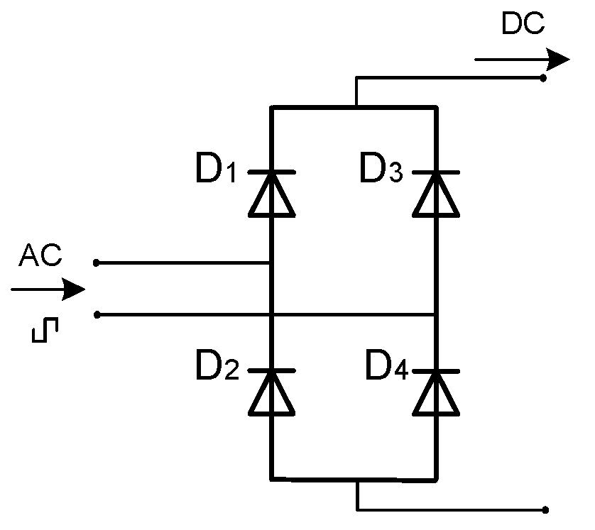
2.3. Diode H-Bridge
In the load side of the full-bridge DC-DC converter is the rectifier diode bridge, as is depicted in
Figure 7. In this work, the bridge was implemented with silicon carbide Schottky diodes due to their capability for high-frequency operation and working voltage of up to 1200 V. Additional advantages of using this type of diodes are the reduction in the specifications for the required heatsink, low commutation losses, and high efficiency. All these characteristics together lead to a high-performance converter.
The losses in the diodes are determined with (11)–(14).
where
FDIODE is the losses in the diode;
VF is the driving voltage of the diode;
IF(AVG) is the current flowing through the diode;
IF(RMS) is the RMS current of the waveform flowing through the diode;
δ is the duty cycle of the diode;
RD(ON) is the on resistance of the diode;
IMAX is the maximum value of current (in forward bias) that flows through the diode; and
IMIN is the minimum value of current (forward bias) flowing through the diode.
The losses in the two stages of the converter (rectifier and inverter) are determined considering the nominal operating conditions of the topology. Equation (1) for the losses of the MOSFETs is made up of two parts, the conduction and switching losses. Conduction losses correspond to the product of the square of PON (3) and POFF (4). The switching losses correspond to the sum of PON (3) and POFF (4). The values of ID(ON), D, fSW, and VDD are determined in the dimensioning of the boost converter.
In this work, VDD is the voltage of the power supply connected to the input of the MOSFET H-bridge, and ID(ON) is the current demanded by the converter. D is the duty cycle to which the semiconductor devices are subjected. The values of RDS(ON), tON, and tOFF were obtained from the manufacturer’s data sheet.
To calculate
PDIODE (11), it is required to determine (12) and (13).
IMIN is the current value demanded by the load connected to the bridge, while
IMAX is twice
IMIN.
VF and
RD(ON) are considered the
VF-
IF characteristic curves of the diode at different temperatures. Therefore, the values of
VF and
RD(ON) are dependent on the temperature and the currents
IMIN and
IMAX. To obtain the final efficiency of the converter, it is essential to determine the output power (
PDCout), which is determined with Equation (14).
where
PDCin is the input power of the converter,
nM is the number of MOSFETs used,
nD is the number of diodes, and
PMFT is the total losses of the medium-frequency transformer.
3. Simulation Results
The data used for the numerical simulation of the converter are reported in
Table 4. The converter is devised for photovoltaic system applications; therefore, it can be interconnected to DC buses, DC microgrids, and/or DC loads. The interconnection interface steps the voltage input up from 42 V to 672 V, a ratio of 16. In all simulations, the converter is supplied by a DC source, and the load is 1680 Ω.
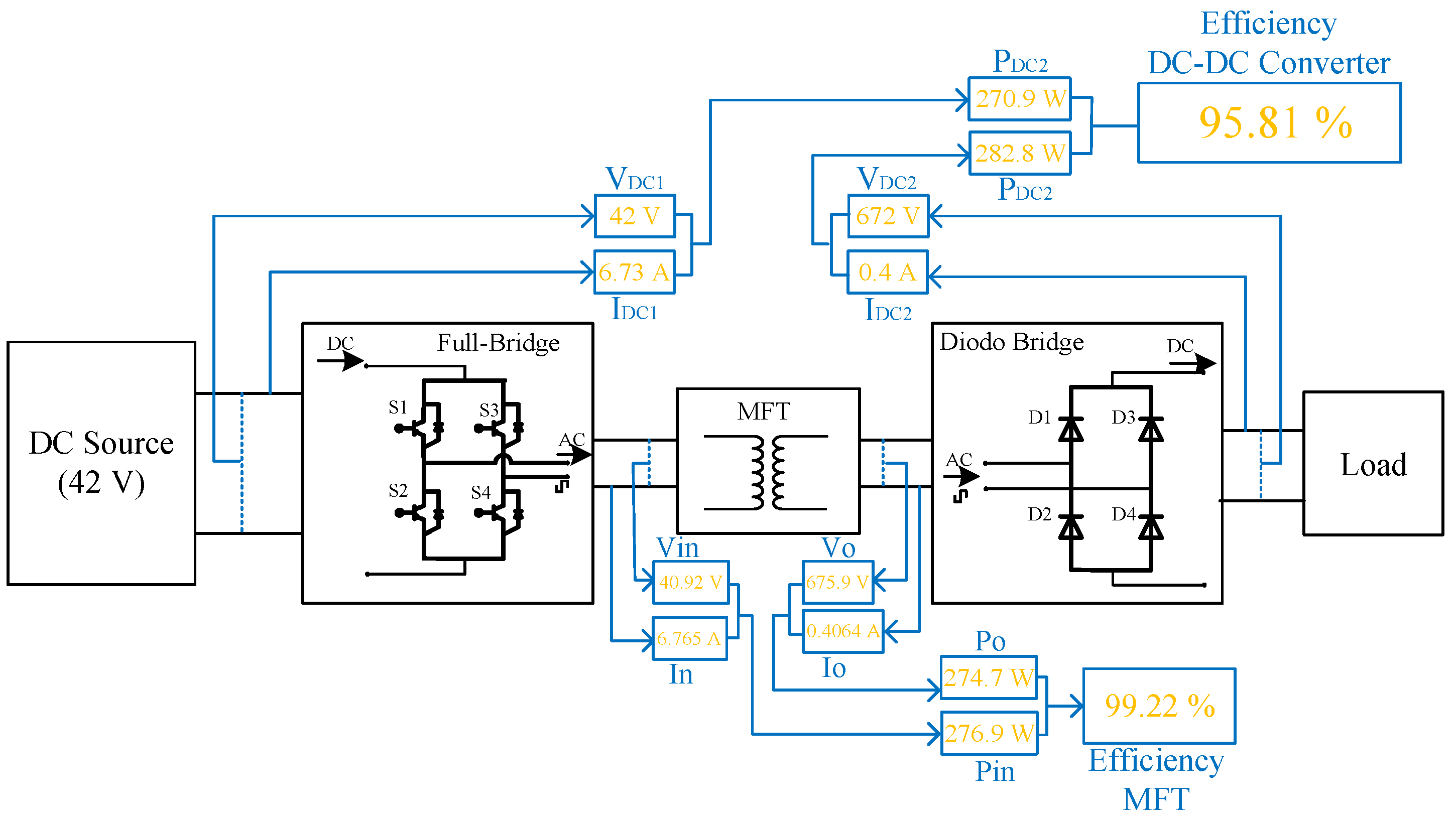
Figure 8 shows the MATLAB-Simulink version R2022b scheme of the proposed converter.
Figure 9 shows the block diagram of
Figure 8.
The parameters of the MFT are reported in
Table 5. In this work, a T equivalent model was used to determine the magnetization inductance and resistance (
Lm,
Rm), the primary and secondary winding dispersion inductances (
Ld1,
Ld2), and the resistance corresponding to the primary and secondary of the MFT windings (
R1,
R2).
Lm and
Rm were calculated with (15) and (16), respectively [
23], and
Ld1 and
Ld2 were determined with (17) [
24], whereas
R1 and
R2 were calculated with (18) and (19), respectively [
21].
A nanocrystalline-core MFT has lower dispersion inductances in comparison to high-frequency ferrite-core transformers. Such low dispersion inductance is because nanocrystalline cores exhibit high permeability, ranging from 15,000 to 150,000, while ferrites have 4000, at most. It is a well-known fact that the greater the permeability, the lower the dispersion inductance. All this leads to lower dispersion flow, and as a consequence, a concentrated magnetic flow occurs at the transformer core, which allows minimum MTF losses. These characteristics mean that greater converter efficiency can be obtained by using nanocrystalline MFT cores instead of ferrite.
where
µr is the relative permeability of the core material,
µ0 is the vacuum permeability, and
lc is the mean length of the core [
23].
where:
= vacuum permeability
dins1 = insulation distance between the layers of the primary winding
dins2 = insulation distance between the layers of the secondary winding
m1 = number of layers in the primary winding
m2 = number of layers in the secondary winding
MLTiso = mean length of the isolation distance
MLTpri = mean length turns of primary portion
MLTsec = mean length turns of secondary portion | diso = isolation distance
NL1 = turns per layer
hw = winding height
dpri = thickness of the primary winding
dsec = thickness of the secondary winding
∆1 = penetration ratio of the primary winding,
∆2 = penetration ratio of the primary winding,
where is the skin depth |
MLT1 and MLT2 are the mean lengths of the primary and secondary windings, respectively. µΩ/cm1 and µΩ/cm2 are the resistance per centimeter of the primary and secondary winding conductors, respectively.
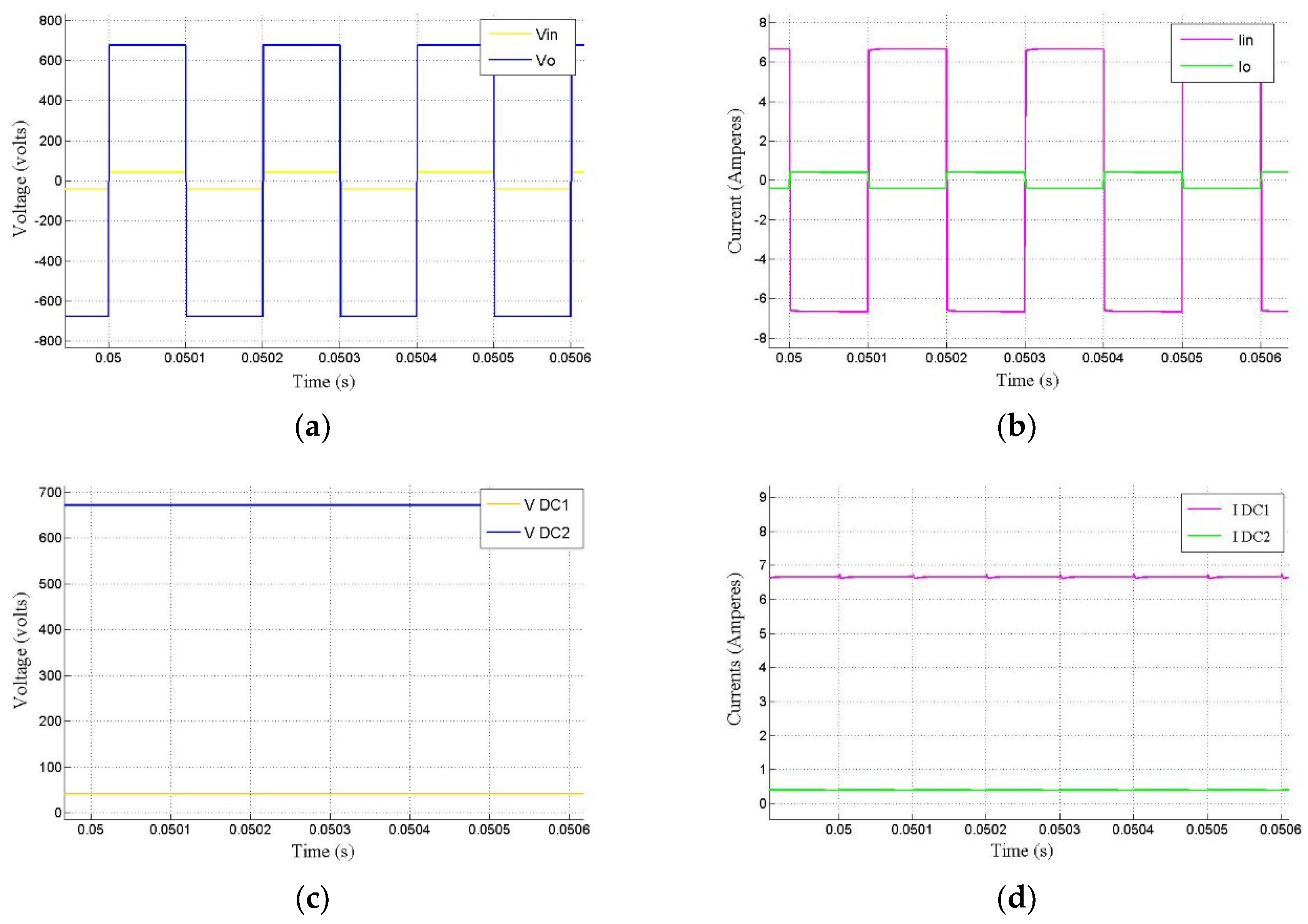
The simulation results are depicted in
Figure 10a–d. In
Figure 9, observe that the input and output MTF voltages are 40.92 V and 675.9 V, respectively; this results in a turns ratio of 16.5. Then,
Figure 9 shows the input and output MFT currents, 6.76 A and 0.406 A, respectively. This yields an efficiency of 99.22%. Next,
Figure 9 depicts both the input and output converter voltages, which are the result of a load of 1680 Ω, and input/output converter voltages of 42 V/672 V, respectively. Finally,
Figure 9 presents the input and output converter currents, 6.73 A and 0.403 A, respectively. The converter efficiency is 95.81%. Various other simulations were performed at distinct frequencies (1 kHz, 5 kHz, 10 kHz, 20 kHz, and 50 kHz) focusing on determining the frequency at which the highest converter efficiency is obtained. This frequency is 20 kHz.
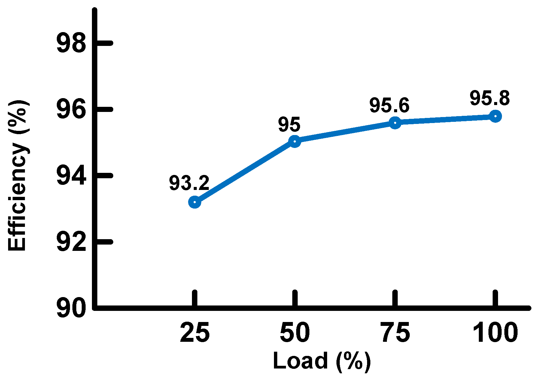
Figure 11 shows the efficiency of the boost converter obtained in the simulation with respect to different load levels. The maximum efficiency is 95.81%. The total converter losses are 4.19%, which is the sum of 0.78% from the MTF plus 3.41% from the MOSFET H. The simulation results confirm that the nanocrystalline-core MFT achieves high converter efficiency. Also notice that the MFT losses are low using square waves at 20 kHz. The MFT high step-up ratio, in addition to its galvanic isolation, makes this proposed converter a very attractive solution in PV system applications.
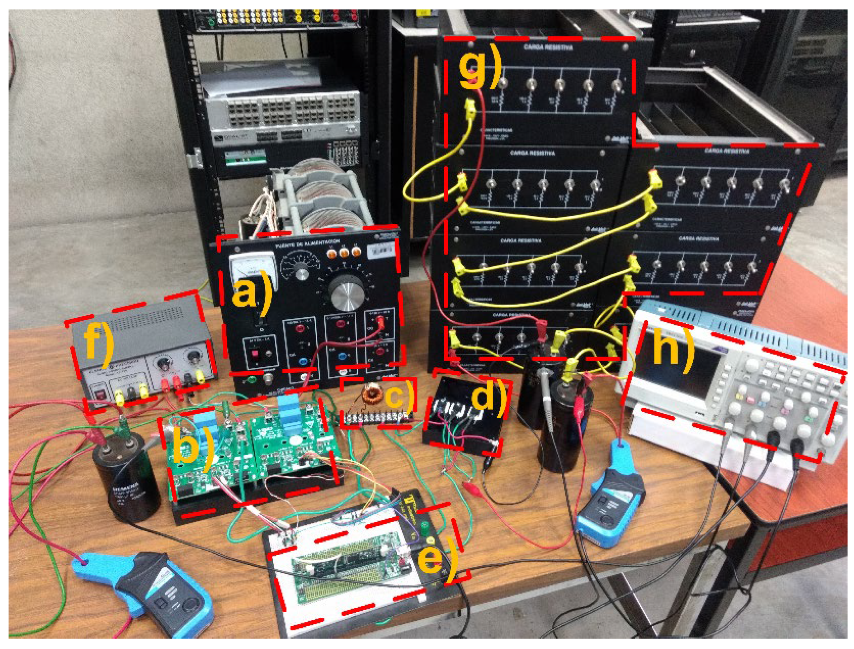
4. Experimental Results
To validate the design and simulation results, a lab prototype of the full-bridge DC-DC converter with a high-efficiency nanocrystalline-core MFT was implemented and tested. The specifications of this lab prototype are reported in
Table 6. Observe that the prototype was tested at 275 W, with a DC input voltage of 42 V and a load of 1680 Ω. The lab prototype is designed to achieve a voltage conversion ratio of 1 to 16.
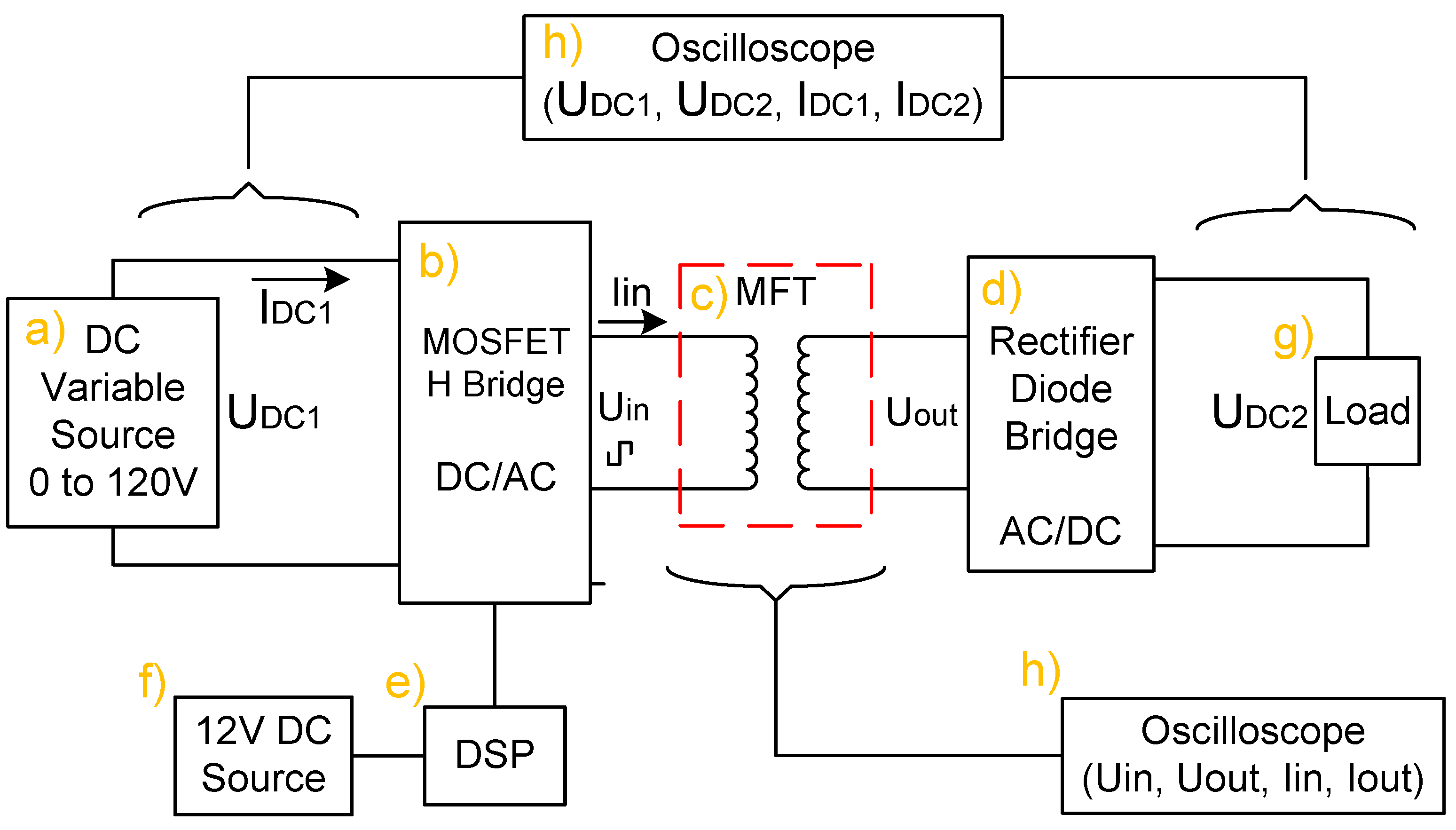
Figure 12 depicts a block diagram of the experimental setup. The converter is fed with a DC variable voltage source. The supplied signal to the MOSFET H-bridge is a square wave at 20 kHz generated with a DSP PICOLO S28335 (TexasInstrument, Dallas, TX, USA).
Figure 13 shows the lab prototype and the experimental setup. The 20 kHz nanocrystalline-core MFT was constructed according to the specifications listed in
Table 7. At this frequency, the commutation losses of the MOSFET H-bridge increases, and converter efficiency drops.
However, if a MFT is designed at frequencies below 20 kHz, the efficiency is still about 95%. In this case, the power density is lower than required, and the size of the transformer can be increased to comply with the amount of power specified.
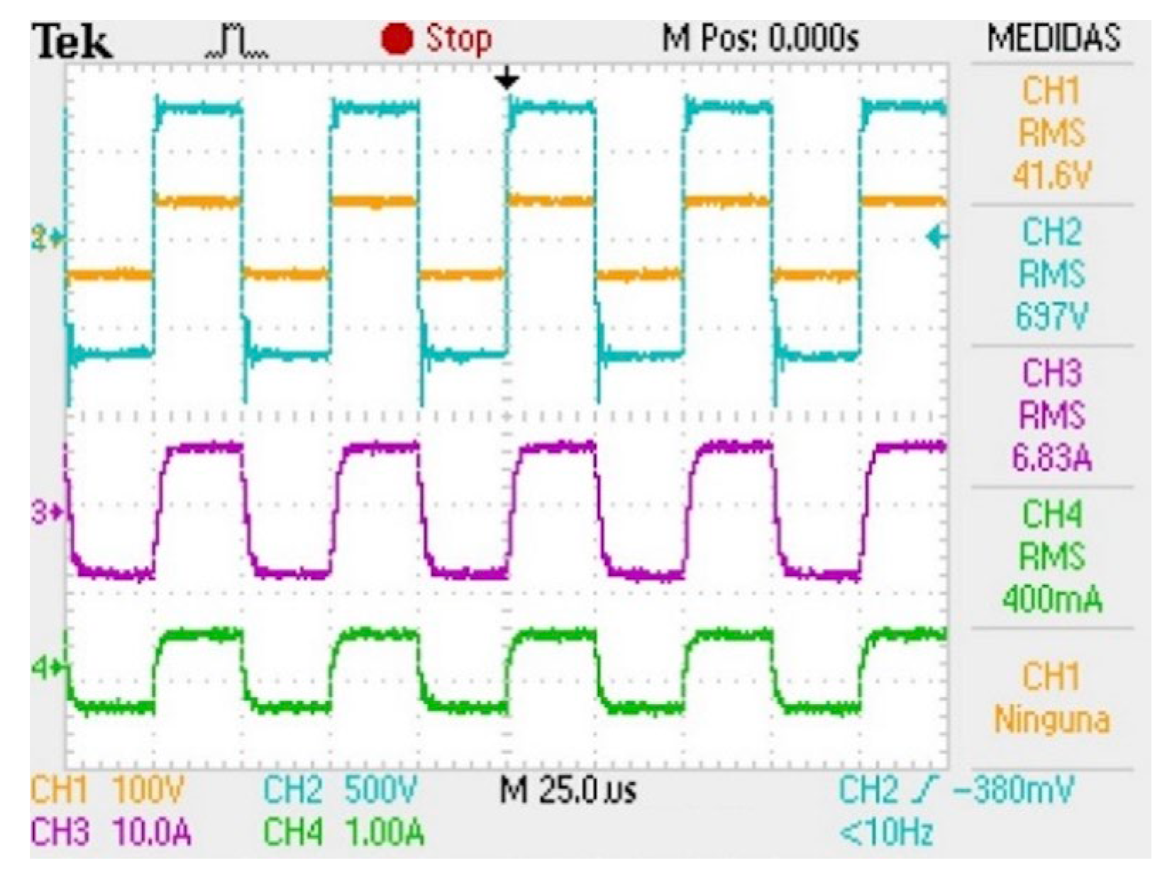
Figure 14 depicts both the voltage and the current MTF waveforms. Observe that the input voltage is 41.6 V, the output voltage is 697 V, the input current is 6.83 A, and the output current is 0.400 A. The final MFT efficiency is 98.12%, which is high compared to other nanocrystalline-core MFTs reported in the literature.
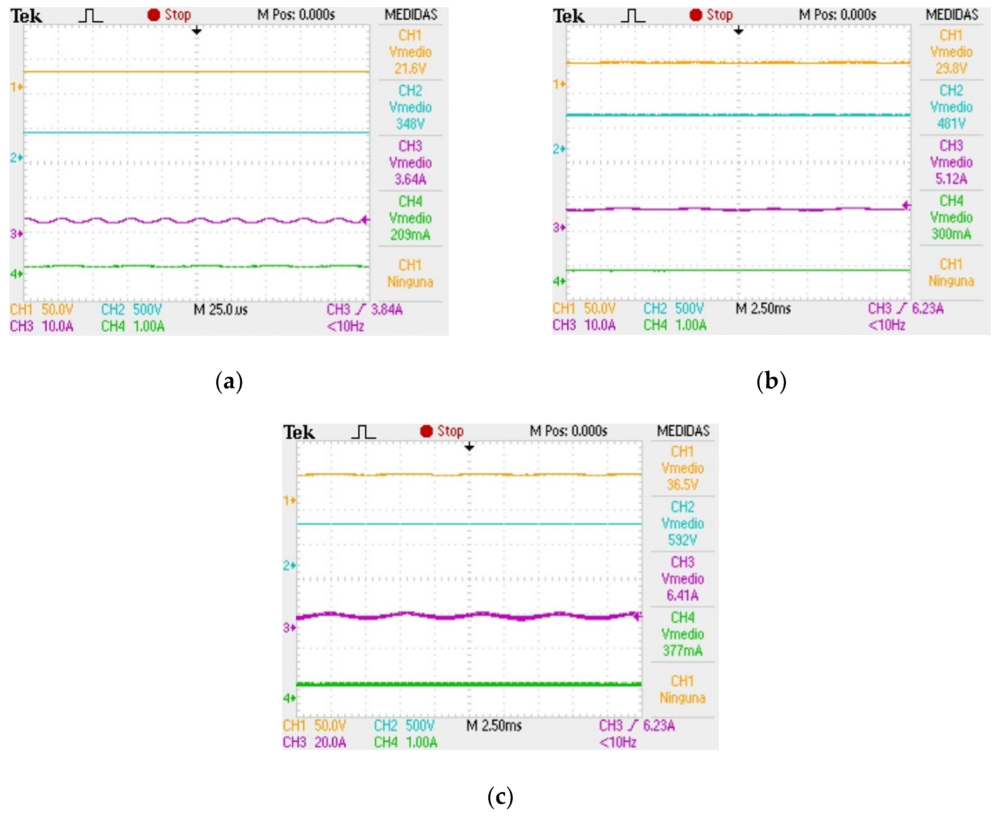
Figure 15a–c show the voltage and current inputs and outputs of the boost converter at 25%, 50%, and 75% load.
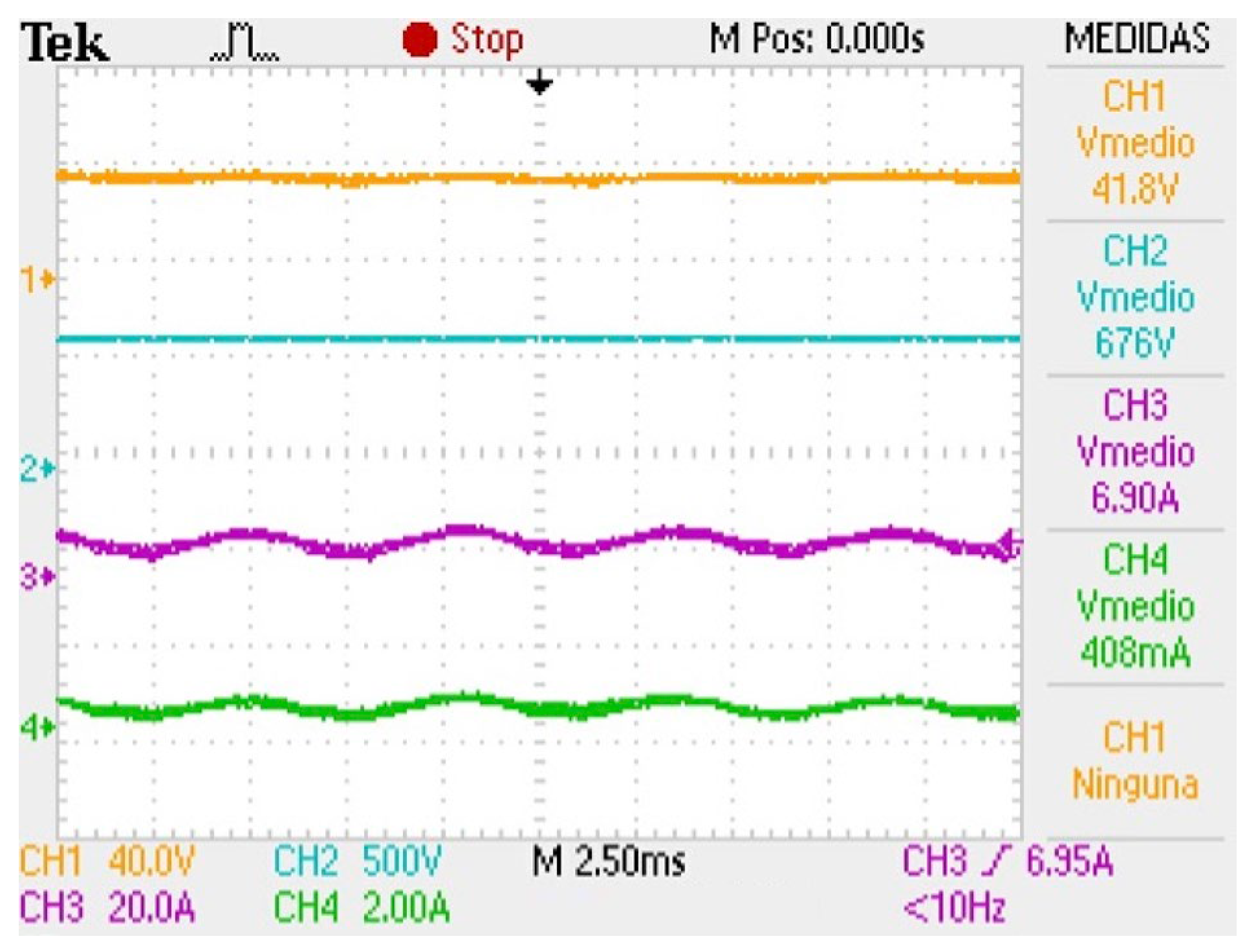
Figure 16 shows the input and output voltages as well as the currents of the DC-DC converter at full load. Notice that the input voltage of the converter is 41.8 V, while its respective output voltage is 676 V. The input current of the converter is 6.9 A, and the output current is 0.408 A. The full-bridge DC-DC converter efficiency is 95.62% at a power of 275 W.
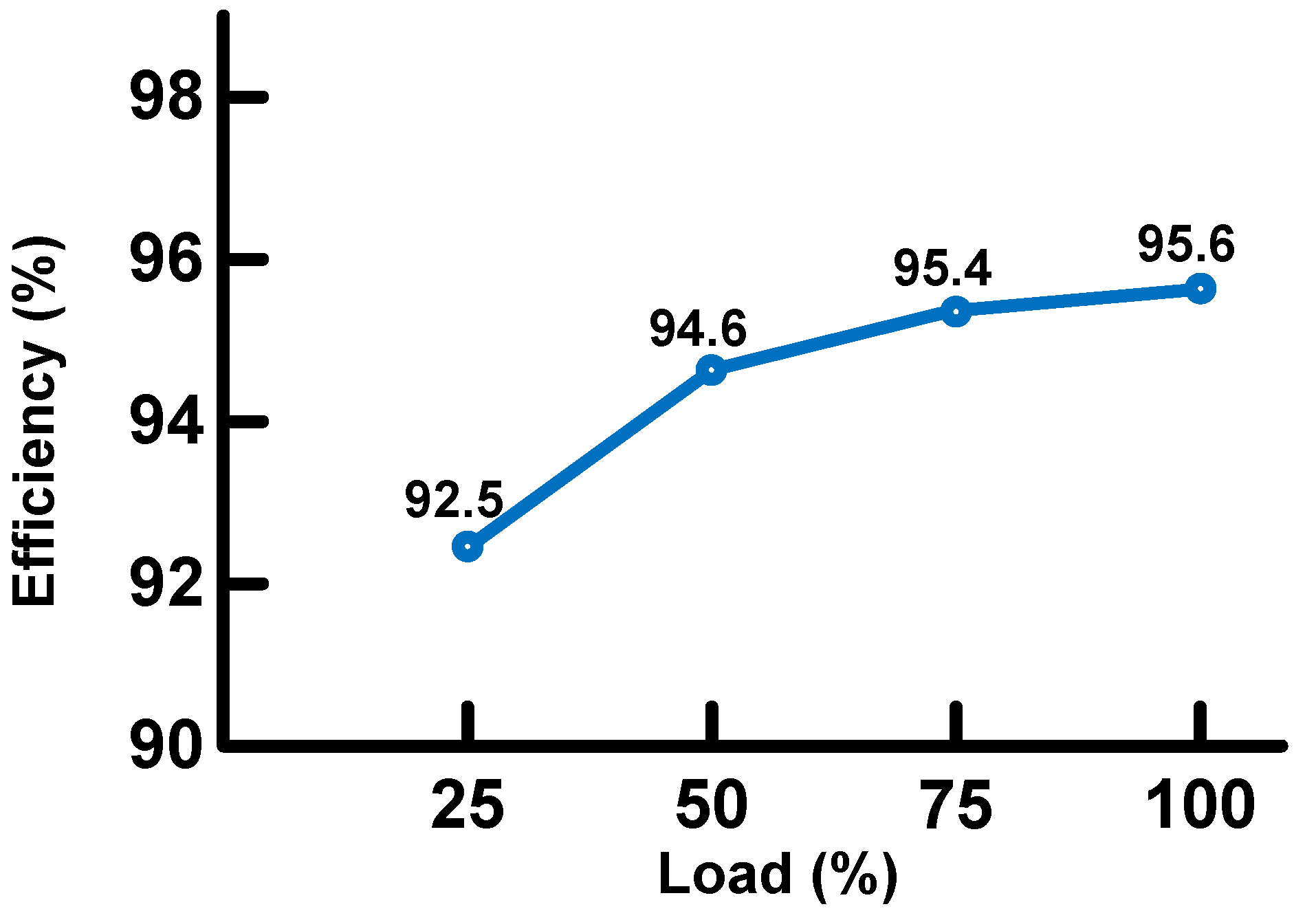
Figure 17 shows the efficiency of the boost converter obtained in the laboratory with respect to different load levels; the highest efficiency obtained is 95.6% at full load.
The experimental results obtained validate the high values of the transformer turns ratio, efficiency, and voltage step-up ratio (1:16) of the DC-DC converter design. These results are very encouraging for the use of the proposed converter as an interface to connect PV systems to DC microgrids, DC buses, and/or loads.
5. Discussion
A review of research papers was thoughtfully carried out to compare our proposal to other similar works also featuring DC-DC converters with a voltage conversion ratio >8 and high efficiency. Considering this,
Table 8 presents the characteristics of five different proposed converters.
Referring to
Table 8, ref. [
4] presents a high voltage gain converter (8.4) with an input voltage of 45 V and an output voltage of 380 V. This design is based on boost and buck–boost converters. However, this proposed converter was validated with a lab prototype specified at 100 W and does not provide galvanic isolation because no transformer is included. The reported converter efficiency is 94.8%. In comparison, the voltage conversion ratio in our proposed converter is 90.5% greater than that reported in [
4], and our converter is slightly more efficient (0.8%).
In [
5], a voltage conversion ratio very close to [
4] is reported but with the advantage of providing internal galvanic isolation. The results were validated using a lab prototype specified at 300 W. The primary and secondary testing voltages are 40 V and 400 V, respectively. The reported efficiency is 94.5%, just 1.1% lower than that achieved in our work. However, the voltage conversion ratio of the converter is 60% lower than that obtained in our work.
In [
7], a DC-DC converter design exhibiting a voltage conversion ratio of 1 to 11.5 is presented. The converter input/output voltage is 34 V/380 V. The reported efficiency is 93% and was validated with a 200 W lab prototype. The voltage conversion ratio achieved in our proposed converter is 39.13% greater, and the efficiency is slightly greater (2.6%). In summary, in [
4,
5,
7], the reported efficiencies are closer to 95%, but the corresponding voltage conversion ratios reported are generally about 35% lower than in our work.
Moreover, refs. [
6,
9] presents proposed DC-DC converters for which voltage conversion ratios greater than 15 have been reported. Specifically, in [
6], a voltage booster with a voltage gain of 15.8 is described. This converter was validated using a 225 kW lab prototype. The input/output voltages are 24 V/380 V with an efficiency of 91.6%. The voltage conversion ratio achieved is 0.2, lower than the ratio reported in our investigation. Also, the reported efficiency is 4% lower. In other work, ref. [
9] presents a galvanic isolated DC-DC converter with a high voltage conversion ratio of 1 to 23. However, the efficiency of 92% achieved is low. In that work, compared to our proposed converter, a slightly higher voltage ratio was obtained but with 3.6% lower efficiency.
In summary, the full-bridge DC-DC converter featuring an MFT with a nanocrystalline core proposed in this paper contributes to increasing the efficiency of photovoltaic systems interconnected to DC microgrids, DC buses, and/or DC loads.


 ,
, 
