Abstract
DC–DC buck converters have been designed by incorporating different control stages to drive the switches. Among the most commonly used controllers, the sliding mode control (SMC) and proportional-integral-derivative (PID) controller have shown advantages in accomplishing fast slew rate, reducing settling time and mitigating overshoot. The proposed work introduces the implementation of both SMC and PID controllers by using the field-programmable gate array (FPGA) device. The FPGA is chosen to exploit its main advantage for fast verification and prototyping of the controllers. In this manner, a DC–DC buck converter is emulated on an FPGA by applying an explicit multi-step numerical method. The SMC controller is synthesized into the FPGA by using a signum function, and the PID is synthesized by applying the difference quotient method to approximate the derivative action, and the second-order Adams–Bashforth method to approximate the integral action. The FPGA synthesis of the converter and controllers is performed by designing digital blocks using computer arithmetic of 32 and 64 bits, in fixed-point format. The experimental results are shown on an oscilloscope by using a digital-to-analog converter to observe the voltage regulation generated by the SMC and PID controllers on the DC–DC buck converter.
1. Introduction
Among the currently available power converters [], DC–DC buck converters are commonly considered in the development of power applications because they provide high efficiency from a relatively simple circuitry. The most simple topology of the DC–DC buck converter consists of six elements that are described in the following section. The DC–DC converter must guarantee a desired voltage () that is taken as the reference to be reached by the output (). This task requires the appropriate design of a controller to reduce the error (). In addition, the design of a controller for the converter must also mitigate overshoot, reduce settling time and increase slew rate. One of the controllers that are case studies in the proposed work is the well-known sliding mode control (SMC), the control law of which is taken from [], where the authors showed the voltage regulation of a DC–DC buck converter accomplishing fast dynamic response, small steady-state output error, and practically zero overshoot.
As recently shown by the authors in [], time simulation is a good option to enhance the response of a controller for a converter. Continuing in this direction, the proposed work applies time simulation methods to approximate the solution of the ordinary differential equations (ODEs) that are modeling the buck converter. The other reason is that the application of numerical methods to solve ODEs is also helpful to synthesize discretized equations on a field-programmable gate array (FPGA) device, as detailed in the proposed work. Interested researchers can read related works that perform the simulation of DC–DC converters by applying numerical methods, as described in [,,,].
The design of SMC controllers requires the definition of a sliding surface, which, in this case, is based on the sign() function, which is synthesized on the FPGA by approximating the error, as detailed in the following sections. Another well-known controller that is considered in the proposed work, just to show the FPGA synthesis and the response when controlling a DC–DC buck converter, is the proportional-integral-derivatve (PID) controller [,,]. In a real application, a PID controller has the challenge of performing a correct tuning of the gains associated to the proportional , integral , and derivative actions [,,]. In this manner, the emulation of a DC–DC buck converter along its controller, like SMC or PID, can be performed on an FPGA board. In fact, this emulation case can also be performed within the topic known as hardware-in-the-loop (HIL) []. Actually, HIL is a fundamental component of the power electronics control design cycle, and it includes the use of FPGAs. For instance, the authors in [,] provide examples on the use of HIL associating time-simulation methods. Therefore, and as one can infer, the HIL and FPGA implementations require the knowledge of numerical methods. Henceforth, this work shows the application of an explicit multi-step method to solve the model of the buck converter, which is controlled by SMC and PID blocks that are simulated by applying numerical methods to allow their synthesis into an FPGA.
The rest of the manuscript is organized as follows. Section 2 shows the DC–DC buck converter topology, the equivalent model consisting of two ODEs, and the numerical method to solve the equations. Section 3 shows the numerical methods that are applied to simulate SMC and PID controllers. Section 4 shows the FPGA emulation of the DC–DC buck converter and the FPGA synthesis of the SMC and PID controllers. Section 5 gives the hardware resource consumptions by using the FPGA Cyclone® IV EP4CGX150DF31C7N, and shows experimental results of the converter using SMC and PID controllers for output voltage regulations of 2.5, 3.3, and 4.1 volts. Finally, the conclusions are summarized in Section 6.
2. DC–DC Buck Converter
Power electronics offer a variety of converter topologies that are suitable for different applications []. Among the DC–DC converters that provide a regulated voltage with a lower value than that from a given input, one can find the well-known buck converter, which is a switched-mode regulator that performs DC–DC conversion with good efficiency. The design of a DC–DC buck converter is relatively simple, with an ease mode of use. It consists of simple circuit elements, and in most cases it is the cheaper solution. The DC–DC buck converter topology consists of six elements, namely: an independent DC voltage supply (E), a switch (), a diode (D), a capacitor (C), an inductor (L), and a resistor (R) that may also be considered as the load. These six electrical circuit elements of the buck converter are connected as shown in Figure 1, where one can see that the regulated output voltage () is taken from the parallel connection of the elements.
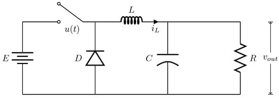
Figure 1.
Circuit elements connection of the DC–DC buck converter topology.
The output voltage of the buck converter must be controlled to provide a desired voltage (). In this case, can be varied by controlling the switch, which can be replaced by a power transistor that has ON–OFF control, or a more complex control stage such as pulse-wide modulation. The model of the converter shown in Figure 1 has two conduction modes: continuous conduction mode (CCM) and discontinuous conduction mode (DCM), which are better described in [,]. In the proposed work, the CCM mode is adopted, which can be modeled by the system of ODEs given in (1).
From the model given in (1), when the control signal makes the action to turn ON or to close the switch, i.e., , the diode is reverse biased and the inductor current has a positive and finite value and when the switch is turned OFF, i.e., , the diode conducts, so that the current through the inductor is uninterrupted between the switch cycles ON and OFF. As a result, in CCM, the inductor current increases and decreases during ON and OFF times of the switch, which, in the proposed work, are manipulated by the SMC [,,,,] or PID [,,,,,] controllers.
The remaining sections use the ODEs given in (2), which basically make a change of variables from (1), where the current state variable is updated to and the voltage state variable to . As the output is associated to , it also belongs to .
The system of ODEs given in (2) has the form of an initial value problem , which requires initial conditions to obtain a solution. The theory on numerical methods can be found in [,], where one can find explicit and implicit ones. In the proposed work, the solution to (2) is performed by applying the second order Adams–Bashforth (AB2) method, which is an explicit multi-step method whose iterative equation is given as follows:
where h is the time step.
3. SMC and PID Controllers
This section describes the selection of parameters of the SMC and PID controllers, and their simulation with numerical methods that will be used to perform the FPGA synthesis in the following section.
3.1. SMC Controller
The model of the DC–DC buck converter given in (2) can be described with a unified state-space formulation in the form of a bilinear system, so that it can be adapted to have the form given in (4).
As already shown in [], the design of the SMC controller can be developed by considering a discontinuous control of the form given in (5),
where s is the scalar switched function defined in the sliding mode theory and the signum function of a real number w, which is a piecewise function that is defined by (6).
As the target of the controller is to provide a constant voltage output , equal to the desired one , then the DC–DC buck converter must be controlled to be in steady state. This can be accomplished through the condition that , and since the desired voltage is a constant value, then . For the sliding mode to exist in the manifold , it needs to satisfy the sliding condition .
As in can be considered to be an input control, then the desired current can be denoted as . However, can be expressed in terms of in order to control the voltage output. This means that the desired current can be expressed by (7),
The SMC requires the definition of a surface s, which can be described by ensuring that tracks the desired current, and therefore, it must accomplish (8),
In this manner, when , the current is in a stable point and the voltage loop is in equilibrium when (9) is accomplished.
In [], the design of the SMC includes both sliding surfaces (8) and (9), meaning that (5) can be applied to both the current and voltage surfaces to obtain (10),
The exponential convergence of the state variables can be achieved by driving the proposed sliding surface s, given in (10), to zero in finite time by means of the control law that is already given in (5). Afterwards, with the goal of forcing the sliding surface during the condition , the control is restricted to take values of 1 or 0. This can be accomplished by deriving a relationship between the compensation parameters and . As a result, the sliding mode locally exists on s = 0, if (11) is satisfied []. In the proposed work, the FPGA synthesis of the SMC is performed by considering the compensation parameters and . In fact, other values of generate unsuitable behaviors, as shown in Figure 2.
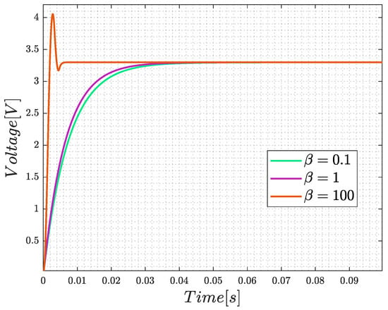
Figure 2.
Voltage response by setting and by choosing three values of .
3.2. PID Controller
Different to the SMC described above, this subsection shows the simulation of the PID controller to be suitable for FPGA synthesis. The design of a PID controller is quite popular due to its simplicity, affordable cost, and suitable efficiency for power converters []. Basically, the PID controller is defined as the weighted linear combination of tracking error, derivative of error, and integral of error in the state variables space. The PID controller acts on the error between the set point or desired value and the current value of the state variable , which is taken as the output, and does not require internal state measurements. The PID controller executes three actions, and therefore it consists of three gain coefficients, namely: proportional , integral , and derivative ones, and its mathematical model is given in (12),
where is the error being controlled and for the DC–DC buck converter, it is defined as,
To perform the FPGA synthesis of the PID controller, the numerical approximation of the integral action is calculated by applying the explicit second order Adams–Bashforth (AB2) method given in (3). The numerical approximation of the derivative action is calculated by applying the difference quotient, which in single-variable calculus, the method is given in (14),
where h is the step-size that must be equal to the one used by the AB2 method given in (3).
4. FPGA Implementation of the SMC and PID Controllers for a DC–DC Buck Converter
Recent works, such as the ones introduced by the authors in [,], show the fast prototyping of SMC controllers using an FPGA. The authors in [] show the FPGA implementation of a PID controller, and very recently, the authors in [] introduced a review on the FPGA implementation of PID controllers. These recent works do not show the FPGA implementation of neither SMC nor PID controllers for a converter. Henceforth, this section introduces the FPGA implementation of SMC and PID controllers for the DC–DC buck converter described in Section 2. In both cases, the converter is emulated into the FPGA by using the circuit values listed in Table 1.

Table 1.
Circuit element values of the DC–DC buck converter shown in Figure 1.
The parameter values of the controllers are taken from the work [] to perform the FPGA synthesis of the SMC, while the parameters of the PID controller were tuned by the authors. In this manner, the parameter values are given in Table 2.

Table 2.
Parameter values of the SMC and PID controllers for the DC–DC buck converter.
4.1. FPGA Implementation of the SMC Controller
The emulation of the DC–DC buck converter is performed by applying the AB2 method given in (3), which requires the selection of a step-size h to guarantee convergence; in this case, it is set to .
The simulation of the SMC is based on (5), whereby combining (7), (8), and (9), then (10) can be updated to,
The scalar switched function s given in (15), and is used to evaluate the response of the SMC according to (5), so that depending on the signum function defined by (6), the controller can take the following values: = 1 if, after evaluating (15), ; = 0.5 if ; and = 0 if .
The digital design of the SMC and the converter are carried out by using computer arithmetic of 32 and 64 bits. Looking at the parameter values given in Table 1 and Table 2, one can see that the maximum value is for = 500, so that this integer number can be represented by using 9 bits. Therefore, by using 32 bits, the fixed-point format can be expressed as 1:9:22, as distributed in Table 3. This implies that one can ensure a resolution of about . A better resolution can be accomplished by using 64 bits, where the fixed-point format can be expressed as 1:9:54.

Table 3.
Distribution of the fixed-point format for the FPGA synthesis of the SMC controller using 32 bits.
The synthesis of the equations for the converter and SMC require some manipulations to identify the best way to perform a block description. As the synthesis is developed by using a step-size of and the AB2 method in (3), then the discretized and reduced expressions for the state variables are given as follows.
In the discretization of the state variable from (2), it is now called and the variables and are updated to and . Therefore, from the first equation in (2): , after applying the AB2 method given in (3), and by using the values of the parameters, the discretized state variable is updated to
In (16), the parameter E is a constant value given in Table 1; however, it is considered a parameter for the FPGA synthesis, as well as the constants , and . Doing the same development for the state variable from (2), it is now called . Therefore, from the second equation in (2), , after applying the AB2 method given in (3), and by using the values of the parameters, the discretized state variable is updated to
In (17), the coefficients of the last equation are also considered parameters, namely: , and . Therefore, once all the parameters are known, the high level description of the converter and the controller are labeled as AB2 and SMC blocks, as shown in Figure 3. The high-level representation shows the block description of the DC–DC buck converter that is emulated by the AB2 method, and the SMC controller. The buses are of 32 bits in fixed-point format and the state variables provided by the AB2 block, are controlled by the SMC block, which generates the signal .
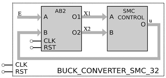
Figure 3.
High-level and block description of the DC–DC buck converter emulated by the AB2 method and the SMC controller, using 32-bit buses for the state variables .
The FPGA implementation of (16) and (17) can be improved by designing single constant multipliers (SCM), as shown in []. This is recommended when a constant multiplies a variable, as for the case of the parameters , and J, which are labeled as SCM in the detailed block description shown in Figure 4. The remaining blocks are adders, subtractors, multipliers, and registers. The control of the iterations n is executed by the design of a finite state machine that is labeled as counter in the block description given in Figure 4.
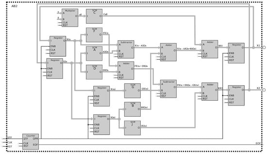
The SMC block shown in Figure 3 is responsible for the control action given in (5). It implements the scalar switched function s given in (15), to take action according to the value provided by the signum function defined by (6), which is synthesized by a comparator. Equation (5) provides three possible output values of the control law , which are . These blocks are shown in Figure 5, which also uses an SCM, an adder, and a comparator.

Figure 5.
Block description of the SMC controller.
4.2. FPGA Implementation of the PID Controller
To perform the FPGA synthesis of the PID controller, the gains of the controller , and , are considered as parameters that have a constant value. On the one hand, and according to the model of the PID given (12), the error must be multiplied by , integrated and multiplied by , and derived and multiplied by . On the other hand, the error is given in (13), having the expression , where according to Table 1, .
In this case, the integral action is simulated by applying the AB2 method given in (3), and the derivative action is simulated by applying the difference quotient method given in (14). The computer arithmetic is performed by using 32 bits that are distributed in the fixed-point format 1:10:21 given in Table 4. As the decimal part has 21 bits, the resolution is about .

Table 4.
Distribution of the fixed-point format for the FPGA synthesis of the PID controller using 32 bits.
The reason to use ten bits in the integer part is to represent the value of , which is the maximum value that can be generated in the data processing. In this manner, the simulation of the DC–DC buck converter is the same as described in the previous subsection, thus, the discretized equations, by applying the AB2 method, are given in (16) and (17). The block description of the converter for FPGA synthesis is shown in Figure 4. In a high-level description, Figure 6 shows the connection of the converter emulated by applying the AB2 method and the PID controller, which takes action on the error to generate the signal , as given in (12). Different to the SMC controller, which generates three output values of the control law , namely: ; the PID controller has a control law that generates two values, namely: .
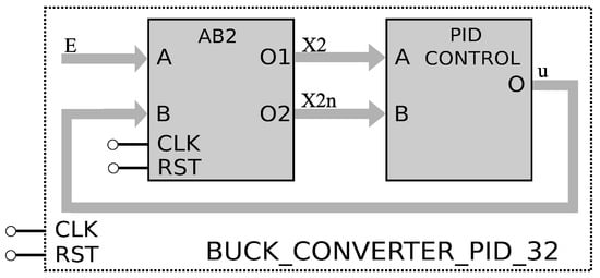
Figure 6.
High-level and block description of the DC–DC buck converter emulated by the AB2 method and the PID controller, using 32-bit buses for the state variables.
The integration action on the error at iteration , denoted as , by applying the AB2 method given in (3), leads to the discretized equations given as follows:
In (18), the parameters and have constant values for the convenience of FPGA implementation. The derivative action is simulated by applying the difference quotient method as given in (14), thus generating the discretized equation given below.
In (19), there is no need to assign a parameter, as done for the previous cases; thus, the constant 860 is used as it is, and it imposes the need of using 10 bits to represent the integer part of a real number, as mentioned above. In this manner, the block description of the discretized equations of the PID given by , (18), and (19) is shown in Figure 7. This FPGA design also requires three clock cycles (CCs) to generate new data at iteration , similar to the FPGA design for the converter using the SMC controller.
5. FPGA Hardware Resources and Experimental Results
The FPGA synthesis of the block descriptions for the emulation of the DC–DC buck converter using SMC or PID controllers requires the hardware resources given in Table 5, by using the FPGA Cyclone® IV EP4CGX150DF31C7N with a 50 MHz clock. The digital blocks described above were designed considering a computer arithmetic of 32 bits. The design of the digital hardware by using 64 bits is quite similar but the hardware resources are higher, as shown in Table 5.

Table 5.
Hardware resources for the synthesis of the SMC and PID controllers for the DC–DC buck converter using 32 and 64 bits, and the FPGA Cyclone® IV EP4CGX150DF31C7N.
It is worth mentioning that, to observe the experimental voltage regulation, the voltage E was emulated as a pulse with a value of during 7000 iterations , and during another 7000 iterations. This emulation allows the observation of the transient response on an oscilloscope, as shown in this section.
5.1. Simulation of Variations and Experimental Results from the FPGA Implementation of the SMC Controller
Figure 8 shows the MatLab transient response and error simulation of the converter by using the SMC parameters given in Table 2.
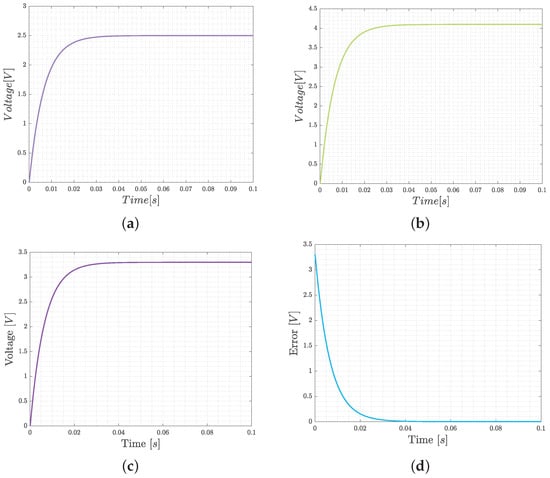
Figure 8.
MatLab simulation results of the buck converter with SMC controller: (a) voltage regulation of 2.5, (b) voltage regulation of 4.1, (c) voltage regulation of 3.3, and (d) evolution of the error.
Figure 9 shows the voltage regulation under 5% of variations in the input voltage E and load of the DC–DC buck converter by using the SMC parameters given in Table 2.
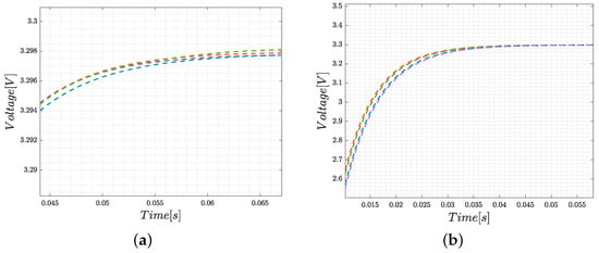
Figure 9.
MatLab simulation of the voltage regulation of 3.3 V, considering 5% variations in the: (a) input voltage and (b) load of the buck converter with SMC controller.
The experimental result from the emulation of the converter and the FPGA implementation of the SMC controller by using a 16-bit digital-to-analog converter, is shown in Figure 10. The figure shows the transient response of the voltage regulation for an output of 3.3 volts, and by emulating the input voltage as a pulse with a value of .
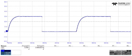
Figure 10.
Experimental observation of the transient response of the voltage regulation of the buck converter with SMC controller.
Figure 11 shows details of the transient response by using the FPGA-based SMC controller for a voltage regulation of 3.3 and 4.1 volts.
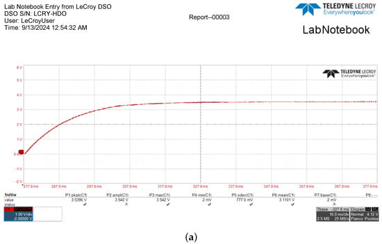
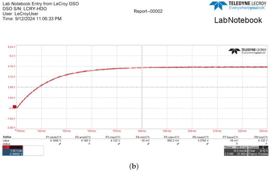
Figure 11.
Details for the experimental observation of the voltage regulation of: (a) 3.3 and (b) 4.1 volts for the buck converter with SMC controller.
5.2. Simulation of Variations and Experimental Results from the FPGA Implementation of the PID Controller
Figure 12 shows the MatLab transient response and error simulation of the converter by using the PID controller parameters given in Table 2.
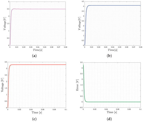
Figure 12.
MatLab simulation results of the buck converter with PID controller: (a) voltage regulation of 2.5, (b) voltage regulation of 4.1, (c) voltage regulation of 3.3, and (d) evolution of the error.
Figure 13 shows the voltage regulation under 5 % variations in the input voltage E and load of the DC–DC buck converter by using the PID controller parameters given in Table 2.
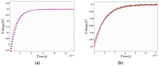
Figure 13.
MatLab simulation of the voltage regulation of 3.3 V, considering 5% variations in the: (a) input voltage and (b) load of the buck converter with PID controller.
The experimental result from the emulation of the converter and the FPGA implementation of the PID controller by using a 16-bit digital-to-analog converter, is shown in Figure 14. The figure shows the transient response of the voltage regulation for an output of 3.3 volts, and by emulating the input voltage as a pulse with a value of .
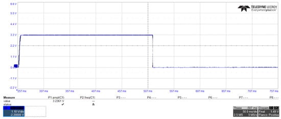
Figure 14.
Experimental observation of the transient response of the voltage regulation of the buck converter with PID controller.
Figure 15 shows details of the transient response by using the FPGA-based PID controller for a voltage regulation of 3.3 and 4.1 volts.
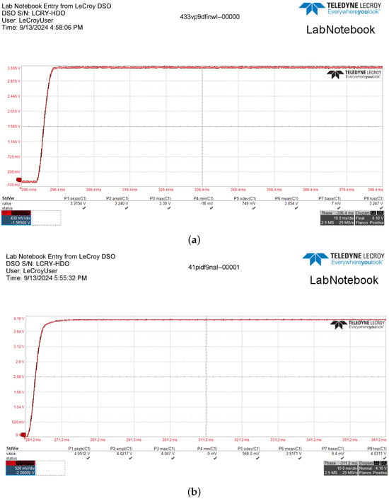
Figure 15.
Details for the experimental observation of the voltage regulation of: (a) 3.3 and (b) 4.1 volts for the buck converter with PID controller.
6. Conclusions
The FPGA implementation of the SMC and PID controllers for a DC–DC buck converter has been shown. The converter was emulated on the FPGA by applying the second-order Adams–Bashforth (AB2) method, and the controllers were simulated by applying their respective control laws. The model for the SMC controller used the signum function, which was synthesized by using a comparator, while the model of the PID controller was synthesized by applying the AB2 method to approximate the integration action, and the difference quotient to approximate the derivative action. In both cases, the FPGA synthesis was performed by using fixed-point format with 32 and 64 bits. The hardware resource consumption was similar for the FPGA implementation of both controllers. Finally, it can be concluded that the experimental observation of the transient response of the voltage regulation for different desired output values and the evolution of the error on an oscilloscope are in good agreement with the theory.
Author Contributions
Conceptualization, E.T.-C.; methodology, S.H.-M.; software, S.H.-M. and J.D.T.-A.; formal analysis, S.H.-M. and E.T.-C.; investigation, S.H.-M. and J.D.T.-A.; writing—original draft preparation, S.H.-M., J.D.T.-A. and E.T.-C.; writing—review and editing, S.H.-M. and E.T.-C.; supervision, E.T.-C. All authors have read and agreed to the published version of the manuscript.
Funding
This research received no external funding.
Data Availability Statement
The original contributions presented in the study are included in the article, further inquiries can be directed to the corresponding author.
Acknowledgments
Sandra Huerta-Moro thanks to CONACyT-Mexico for the PhD scholarship at INAOE. Jonathan Daniel Tavizón Aldama thanks to the scientific Delfin’s program 2024. Esteban Tlelo-Cuautle is on Sabbatical Leave at CINVESTAV supported by CONAHCyT-Mexico: Apoyos Complementarios para Estancias Sabaticas Vinculadas a la Consolidacion de Grupos de Investigacion, in 2023.
Conflicts of Interest
The authors declare no conflicts of interest.
References
- Gonzalez-Prieto, J.A. Finite time adaptive smooth nonlinear control of DC-DC buck converters operating in CCM and DCM. Int. J. Dyn. Control 2023, 11, 619–636. [Google Scholar] [CrossRef]
- Huerta-Moro, S.; Martínez-Fuentes, O.; Gonzalez-Diaz, V.R.; Tlelo-Cuautle, E. On the Sliding Mode Control Applied to a DC-DC Buck Converter. Technologies 2023, 11, 33. [Google Scholar] [CrossRef]
- Alsarayreh, S.; Suto, Z. Optimal Selection of Switch Model Parameters for ADC-Based Power Converters. Energies 2024, 17, 56. [Google Scholar] [CrossRef]
- Usta, M.A.; Sahin, E. Detailed analysis and modeling of an improved cascade buck converter. Int. J. Electron. 2023. [Google Scholar] [CrossRef]
- Yang, X.; Zhao, L.; Tan, Z.; Zhao, M.; Ding, Y.; Li, W.; Lu, Y.; Qu, W. A High-Efficiency Wide Output Range Reconfigurable Capacitive-Sigma DC-DC Converter. IEEE J. Solid-State Circuits 2023, 59, 1532–1542. [Google Scholar] [CrossRef]
- Hinov, N.; Grigorova, T. Design Considerations of Multi-Phase Buck DC-DC Converter. Appl. Sci. 2023, 13, 11064. [Google Scholar] [CrossRef]
- Sun, M.; Chen, C.; Wang, L.; Xie, X.; Wang, Y.; Xu, M. A Fast Transient Adaptive On-Time Controlled BUCK Converter with Dual Modulation. Micromachines 2023, 14, 1868. [Google Scholar] [CrossRef]
- Wu, Q.; Liu, Z.; An, F.; Liu, B. Self-tuning PID feedback control method for magnetic suspension active vibration isolation system with parameters uncertainty. J. Vib. Control 2024, 10775463241228018. [Google Scholar] [CrossRef]
- Yang, Y.; Chen, Y.; Zhang, B. A simplified model-based nonlinear control with fast response and simple design flow for HB-LLC resonant converter. Int. J. Circuit Theory Appl. 2024, 52, 4535–4555. [Google Scholar] [CrossRef]
- Covaciu, F. Development of a control program for dc motors using pid control and low-pass filter. Acta Tech. Napoc. Ser. Appl. Math. Mech. Eng. 2023, 66, 191–198. [Google Scholar]
- Liu, J.; Chen, S.; Cai, S.; Xu, C. A proposal on centralised and distributed optimisation via proportional-integral-derivative controllers (PID) control perspective. IET Cyber-Syst. Robot. 2023, 5, e12100. [Google Scholar] [CrossRef]
- Wang, L.; Luo, Y.; Yan, H. Ant colony optimization-based adjusted PID parameters: A proposed method. PeerJ Comput. Sci. 2023, 9, e1660. [Google Scholar] [CrossRef] [PubMed]
- Ding, F.; Zhang, W.; Luo, X.; Hu, L.; Zhang, Z.; Wang, M.; Li, H.; Peng, M.; Wu, X.; Hu, L.; et al. Gain self-adjusting single neuron PID control method and experiments for longitudinal relative position of harvester and transport vehicle. Comput. Electron. Agric. 2023, 213, 108215. [Google Scholar] [CrossRef]
- Acosta-Rodriguez, R.A.; Martinez-Sarmiento, F.H.; Munoz-Hernandez, G.A.; Mino-Aguilar, G.; Portilla-Flores, E.A.; Nino-Suarez, P.A.; Salcedo-Parra, O.J. Validation of Sliding Mode and Passivity Control in High-Power Quadratic Buck Converter through Rapid Prototyping. IEEE Access 2024, 12, 8668–8699. [Google Scholar] [CrossRef]
- Garcia-Vellisca, M.A.; Munoz, C.Q.G.; Martinez-Garcia, M.S.; de Castro, A. Automatic Word Length Selection with Boundary Conditions for HIL of Power Converters. Electronics 2023, 12, 3488. [Google Scholar] [CrossRef]
- Zheng, M.; Chen, C.; Zhang, Y.; Ruan, M.; Li, P. Event-Triggered Fractional PID-Based Load Frequency Control in Islanded Microgrids under Cloud-Edge Collaborative Framework. J. Circuits Syst. Comput. 2024, 33, 2450167. [Google Scholar] [CrossRef]
- Ashok, B.; Michael, P.A. Integration of cascaded controllers for super-lift Luo converter with buck converter in solar photovoltaic and electric vehicle. Analog. Integr. Circuits Signal Process. 2024, 118, 449–466. [Google Scholar] [CrossRef]
- Xiang, B.; Mao, X.; Liu, Z.; Wang, H. Stabilization of isolated hybrid microgrids with electric vehicle-based energy storage systems using a fractional order proportional-integral-derivative control. Int. J. Green Energy 2023, 21, 2155–2165. [Google Scholar] [CrossRef]
- Sangeetha, S.; Revathi, B.S.; Balamurugan, K.; Suresh, G. Performance analysis of buck converter with fractional PID controller using hybrid technique. Robot. Auton. Syst. 2023, 169, 104515. [Google Scholar] [CrossRef]
- Burden, R.L.; Faires, J.D.; Burden, A.M. Numerical Analysis; Cengage Learning: Boston, MA, USA, 2015. [Google Scholar]
- Chapra, S.C.; Canale, R.P. Numerical Methods for Engineers; Mcgraw-Hill: New York, NY, USA, 2011; Volume 1221. [Google Scholar]
- Ghamari, S.M.; Khavari, F.; Mollaee, H. Lyapunov-based adaptive PID controller design for buck converter. Soft Comput. 2023, 27, 5741–5750. [Google Scholar] [CrossRef]
- Tarkhani, R.; Krim, S.; Mimouni, M.F. Rapid Prototyping and Hardware-In-the-Loop Verification of Enhanced Sliding Mode Control of an Asynchronous Machine Using a Xilinx System Generator and an FPGA-Zynq Board. Electr. Power Components Syst. 2024. [Google Scholar] [CrossRef]
- Ramakrishnan, B.; Tamba, V.K.; Metsebo, J.; Ngatcha, D.T.; Rajagopal, K. Control, synchronisation and antisynchronisation of chaos in two non-identical Josephson junction models via sliding mode control and its FPGA implementation. Pramana-J. Phys. 2023, 97, 46. [Google Scholar] [CrossRef]
- Zhang, Z.; Nan, Q. Adaptive Network-Based Fuzzy Inference System-Proportional-Integral-Derivative Controller Based on FPGA and Its Application in Radiofrequency Ablation Temperature Control. Appl. Sci. 2024, 14, 4510. [Google Scholar] [CrossRef]
- Ali, A.; Bingi, K.; Ibrahim, R.; Devan, P.A.M.; Devika, K.B. A review on FPGA implementation of fractional-order systems and PID controllers. AEU-Int. J. Electron. Commun. 2024, 177, 155218. [Google Scholar] [CrossRef]
- Tlelo-Cuautle, E.; De La Fraga, L.; Rangel-Magdaleno, J. Engineering Applications of FP-GAs; Springer: Cham, Switzerland, 2016. [Google Scholar]
Disclaimer/Publisher’s Note: The statements, opinions and data contained in all publications are solely those of the individual author(s) and contributor(s) and not of MDPI and/or the editor(s). MDPI and/or the editor(s) disclaim responsibility for any injury to people or property resulting from any ideas, methods, instructions or products referred to in the content. |
© 2024 by the authors. Licensee MDPI, Basel, Switzerland. This article is an open access article distributed under the terms and conditions of the Creative Commons Attribution (CC BY) license (https://creativecommons.org/licenses/by/4.0/).
