1. Introduction
Entering an era marked by surging connectivity demands and data prerequisites, the introduction of the 5G-II band signifies a significant advancement. This innovative iteration in wireless communication operates within the designated frequency range of the 5G-II band, finely tuned to address the specific requirements of swift data transmission, minimal latency, and seamless connectivity. This exploration aims to unveil the capabilities and significance of the 5G-II band, shedding light on its potential to reshape contemporary communication and usher in a future where connectivity knows no bounds.
In the field of wireless communications, a diverse range of antenna designs with unique shapes and characteristics are extensively used. These designs, consisting of semi-circular and U-shaped antennas, are documented in various sources [
1]. A T-shaped structure has been employed to resonate at the higher mode (28 GHz), as reported in [
2]. As discussed in [
3], a complete ground plane is implemented to ensure a stable radiation pattern. Researchers have actively explored techniques to enhance antenna performance, with a notable strategy involving the manipulation of the antenna’s ground plane through the incorporation of parasitic elements, which has been proven to boost antenna performance significantly [
4]. Introducing a slot in the microstrip line increases the resonance in both modes [
5]. Another study presents a rectangular microstrip antenna designed for 5G-band applications [
6]. Additionally, the integration of small fractal components has been explored to contribute to overall improvements in antenna attributes. Circular and U-shaped slots have also been integrated into designs, impacting parameters such as bandwidth and radiation patterns [
7].
Advancements in aerospace communication systems have been achieved through previous research efforts that extended their operational range. Innovative adaptations to antenna designs played a pivotal role in these advancements. For instance, adjustments to a patch antenna with a defective backside and semi-circular slots led to a breakthrough, broadening the bandwidth to align with aerospace communication demands [
8,
9]. Manipulating the antenna’s backside with modified slots yielded unexpected advantages, highlighting the intricate nature of antenna design. Beyond these discoveries, studies have explored alternative alterations to antenna designs, such as using a flexible antenna with a “circular” configuration [
10]. Better gain is achieved by incorporating a center cut in the main patch of the antenna [
11].
Prior research has improved aircraft communication systems by increasing their functional capacity. Creative antenna design changes enabled these advances. Researchers improved a patch antenna with a defective backside by adding semi-circular slots [
12,
13]. Researchers carefully altered the antenna’s structure to increase its bandwidth for aircraft communication.
Historical research has advanced wireless communication systems, particularly by increasing their effective range. Modifications to the constructive antenna design have increased the capacity. This was enhanced by adding semi-circular slots to the patch antenna with a defective ground structure [
14]. Incorporating an oval shape with two adjacent perpendicular rectangular strip lines facilitates proper impedance matching, which contributes to antenna resonance in lower-order bands [
15]. For stable polarized radiation, a centrally fed, U-slot cut has been designed [
16]. Innovative planar CPW-fed trapezoidal monopole antennas have been developed to reduce interference in wireless communications systems operating at 3 GHz and 3.5 GHz, featuring single- and dual-band rejection capabilities. [
17]. These results demonstrate the complexity of antenna design and the potential benefits of unexpected changes. Based on these critical discoveries, research has focused on several antenna design strategies to enhance performance. An exciting investigation concerns the use of a flexible antenna in combination with a radiator designed in a “dumbbell” shape [
18]. This work presents a straightforward design of a penta-band circularly polarized ultra-wideband (PBCP-UWB) antenna on FR4, which exhibits a remarkable fractional axial ratio and impedance-matched bandwidth. The simplicity of the antenna underlines its admirable radiation efficiency, evidenced by consistent results in both measurements and simulations [
19]. Addressing the ecological impact of plastic substrates in wearable 5G and 6G devices, our study presents a biocompatible planar inverted-F antenna (PIFA) with a dielectric constant of 5 on a chitosan substrate. It operates in the sub-6 GHz band at 4.5 GHz. The compact antenna (mm
2) achieves a specific absorption rate (SAR) of 0.41 W/kg, highlighting the potential of chitosan as an eco-friendly dielectric for plastic-free antennas in Internet of Healthcare Things (IoHT) applications [
20]. An interesting investigation related to the use of a flexible antenna in combination with the partial ground plane for ultra-wideband is reported in [
21].
An ‘E-I’-shaped microstrip antenna is designed explicitly for proper impedance matching, which aids resonance in high frequencies ranging from 57.9 to 62 GHz [
22]. A prototype consisting of a dual-polarized L-shaped probe-fed stacked patch antenna and a 16-element phased array is designed for 60-GHz antenna-in-package (AIP) applications. It tackles fabrication challenges by employing an organic multilayer high-density interconnect process [
23]. As described in [
24], adopting a T-shaped structure is used to achieve a stable radiation pattern. A square-shaped patch can increase the bandwidth of a 5G antenna [
25]. This design modification was developed to increase current distribution within the antenna, ultimately improving performance characteristics. Innovative design modifications reflect the iterative and future-oriented essence of antenna engineering [
26].
Resolving the difficulties associated with impedance matching is necessary to transfer power effectively. This can be achieved by including multiple slots in the antenna structure [
27]. This approach helps to achieve excellent impedance matching and allows efficient power transfer in antenna systems [
28]. The efforts outlined demonstrate a continued dedication to advancing antenna engineering. In this area, continued study and innovation are essential to overcome obstacles and maximize the efficiency of aircraft communication systems.
The implementation of the L-shaped design has been crucial in mitigating band resonance problems and improving the antenna’s effectiveness within a specific frequency range [
29]. Research has investigated the shortening of the antenna’s ground plane to increase the range of frequencies it can operate on, thereby modifying the way the signal travels to cover a wider frequency range. Researchers have also focused on modifying the primary patch of the antenna to achieve heightened gain, reshaping the core element to optimize signal concentration and radiation efficiency for overall performance enhancements.
In the context of antenna design for UWB band and 5G and beyond communication systems, a key challenge lies in developing compact antenna structures operating efficiently in the microwave band. This challenge necessitates innovative designs offering improved performance, reduced form factor, and compatibility with the stringent requirements of 5G networks. Our research addresses this challenge by introducing a compact ‘UWB band’ antenna for microwave applications in 5G systems. The subsequent sections of this paper detail the proposed antenna design, its geometry, material selection, design evolution, and parametric study, presenting the results and analysis of the antenna’s performance, concluding with applications in the next section.
2. Geometry and Design Structure
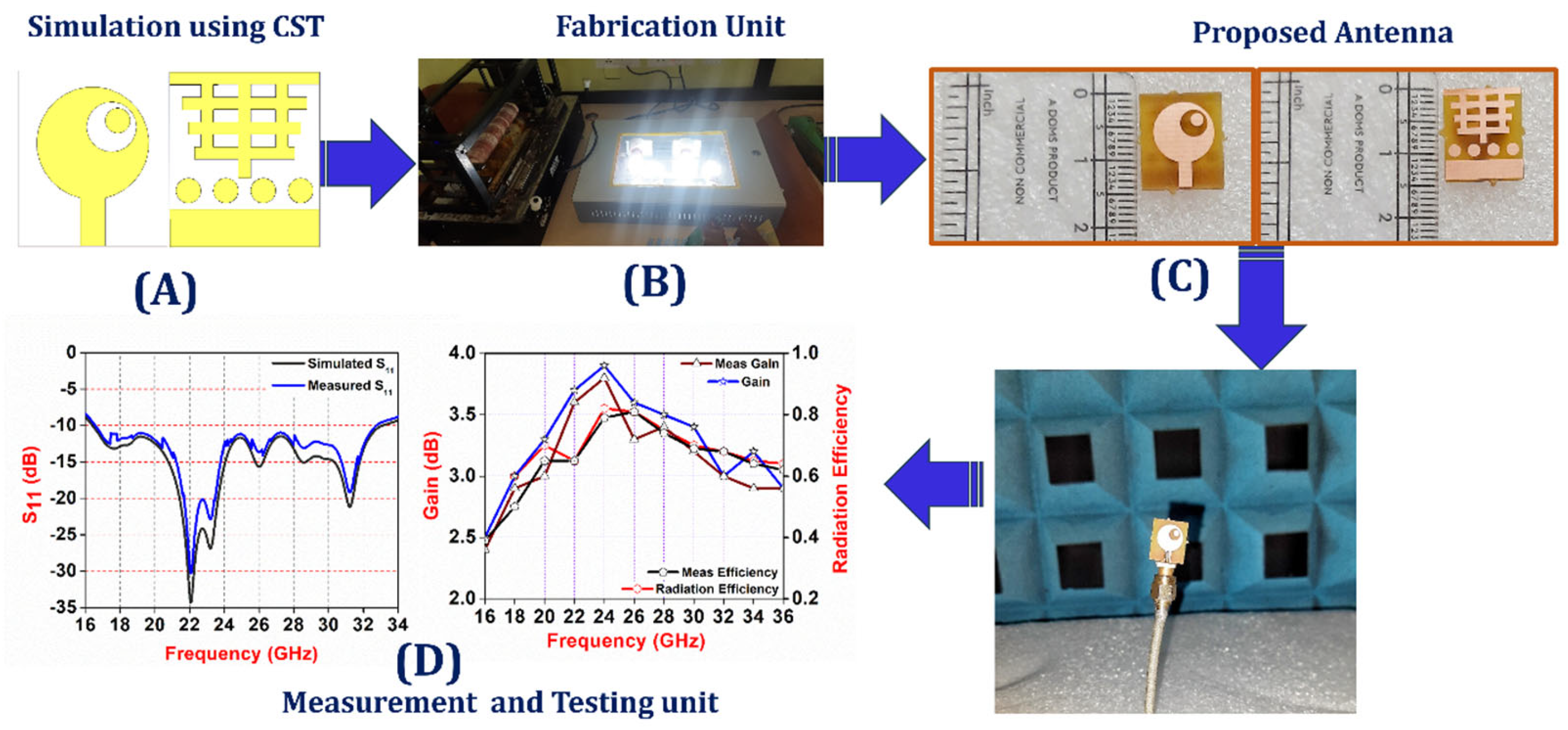
Figure 1 provides a visual representation encapsulating the key stages of the pro-posed antenna’s design and the main elements discussed in this article. The customized antenna under scrutiny boasts dimensions of 12 × 14 × 1.6 mm
3 and is constructed on an FR4 substrate. Copper is chosen as the material for the antenna, and annealing is applied to enhance its permittivity and conductivity. The FR4 substrate, with a measured dielectric constant of 4.3, serves as the foundational material for the antenna.
Simulations are carried out using the CST simulator to assess the antenna’s performance. The antenna laboratory uses conventional chemical etching techniques to perform the fabrication process. Subsequent testing and measurements take place in an anechoic chamber with the assistance of a Vector Network Analyzer (VNA).
The development of this compact antenna tailored for the 5G-II band and beyond holds paramount significance for the progression of wireless communication systems. The chosen dimensions, substrate material, and fabrication techniques underscore a meticulous approach to antenna design, while the evaluation through simulations and practical testing emphasizes the commitment to ensuring optimal performance in real-world communication scenarios.
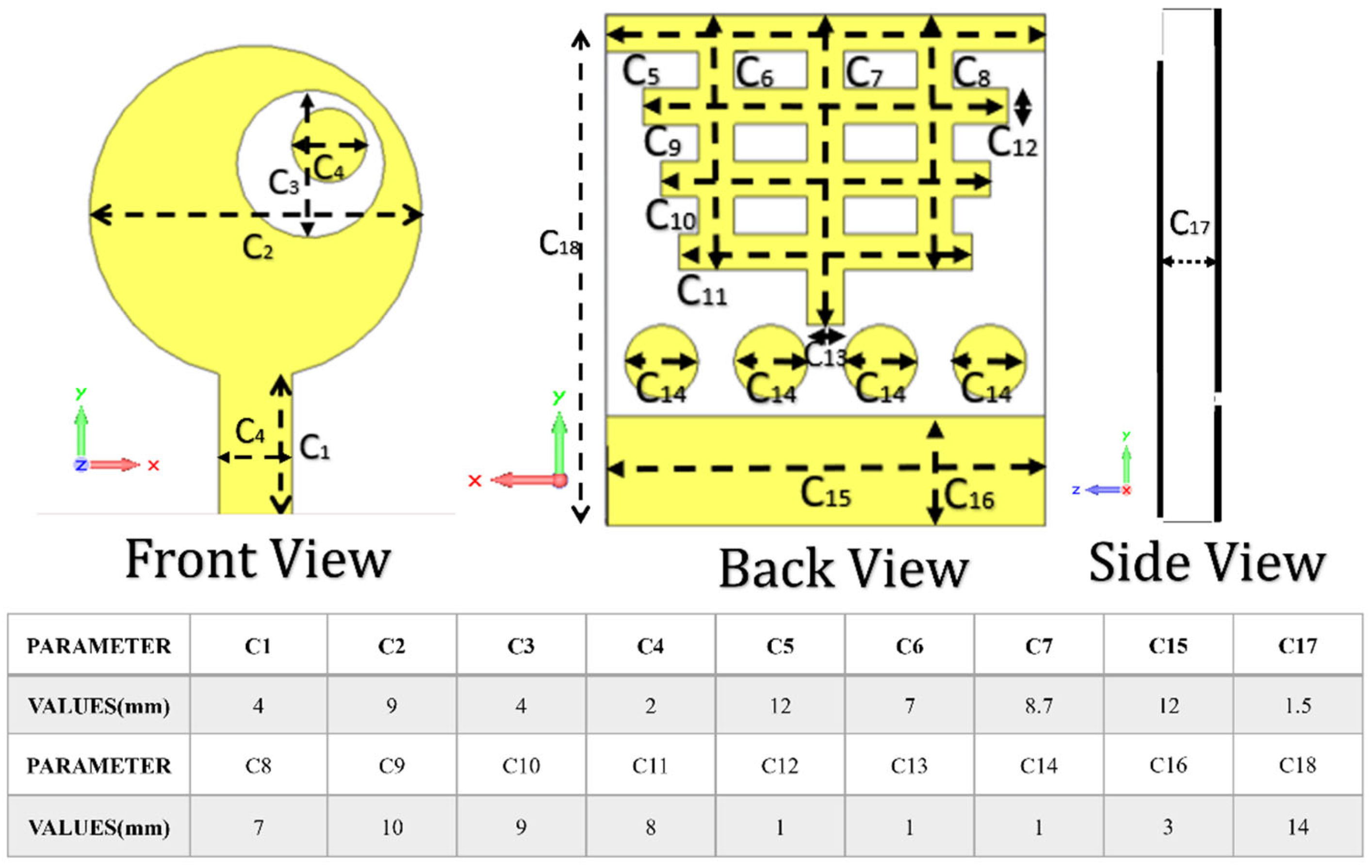
Figure 2 visually represents the antenna design’s geometry and underlying concept. The antenna exhibits a compact yet intricate structure, comprising various front and back elements. On the front side, the design incorporates a circular patch with an interesting twist, namely a circular slot at one of the patch’s corners. Another circular element is positioned within this slot, receiving its central feed via a 50 ohm strip line, contributing to the antenna’s lower bound oscillation. Moving to the back side of the antenna, a distinctive mesh-like structure is observed atop the ground plane. Additionally, four parasitic circular elements are strategically integrated on the underside of the backplane, facilitating the resonance for the higher bound frequencies.
The antenna’s length, height, and width are denoted as ‘C15′ ‘ C18,’ and ‘C17′, respectively. Detailed parameter values for the design are provided in
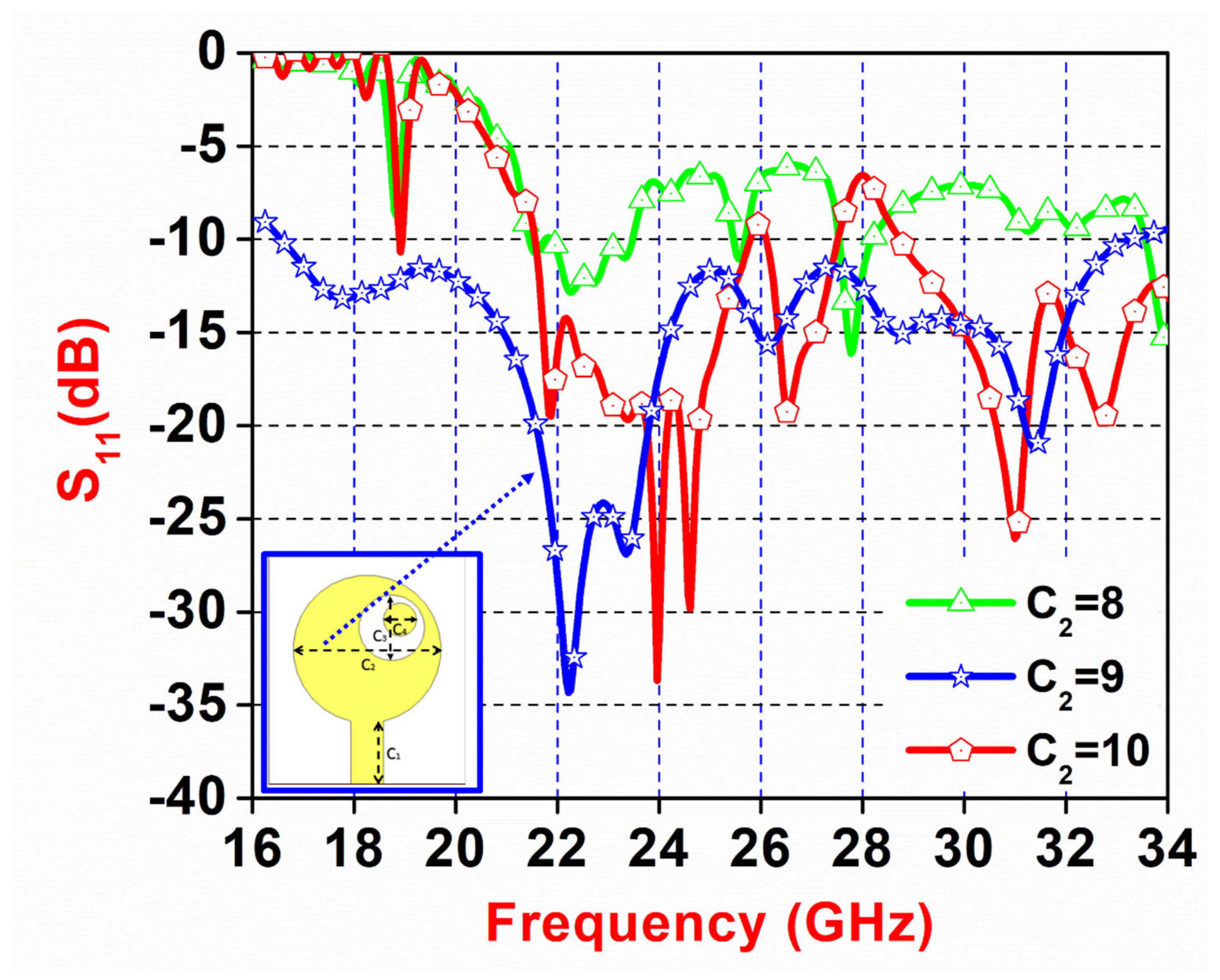
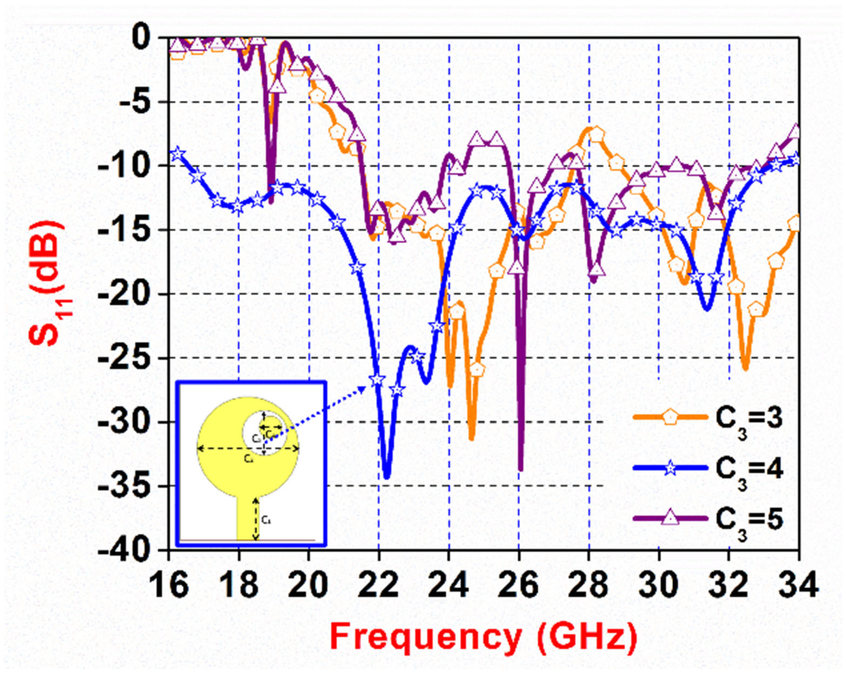
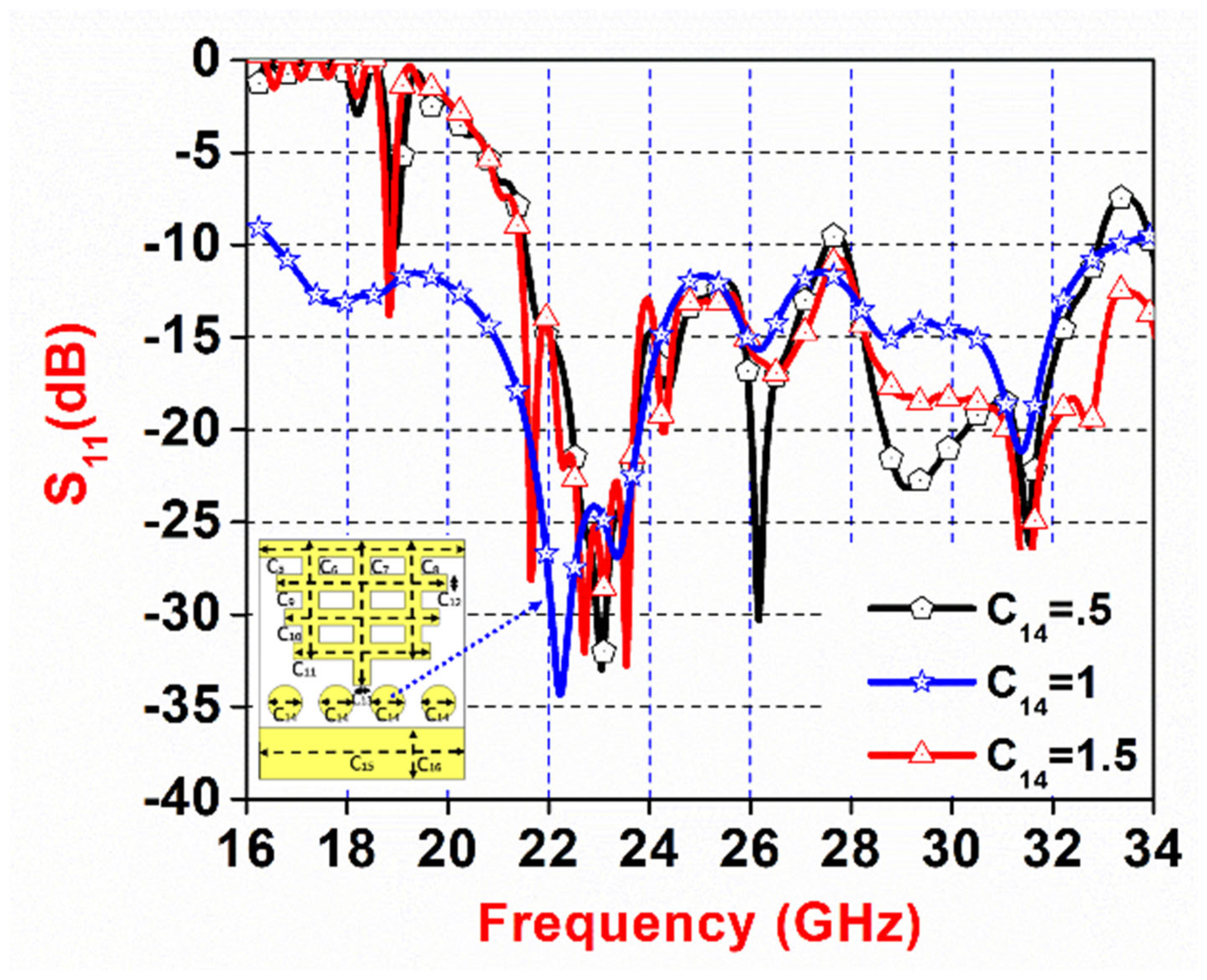
Figure 2. This section offers an in-depth examination of the specifications for the proposed radiator. It outlines the creation of a distinctive configuration incorporating a circular component called ‘C2’. This circular element is securely affixed to the primary microstrip and possesses dimensions represented by ‘C4 × C1’. To further enhance the performance of the lower-order band, a circular slot is introduced, housing a circular parasitic element within it. On the rear side of the radiator, we encounter a mesh-like structure designated as ‘C5 to C12’, which integrates four additional parasitic circular elements with a diameter specified as ‘C14’. These elements contribute to the facilitation of higher-order resonance.
The fabrication process for this proposed antenna design involved using a well-established and highly precise chemical etching technique. Great care was taken in optimizing the fabrication process to ensure utmost precision and repeatability. Subsequently to fabrication, meticulous inspection protocols were meticulously applied to thoroughly scrutinize the antenna for any possible manufacturing defects or irregularities. The aforementioned cutting-edge approach demonstrates a comprehensive and intricate strategy to enhance the antenna’s performance, achieved through meticulous design selections, advanced fabrication methodologies, and rigorous quality control procedures. This methodology stands as a notable advancement within the realm of antenna engineering, pushing the limits of achievable precision, efficiency, and dependability.
3. Design Evolution of the Proposed Antenna
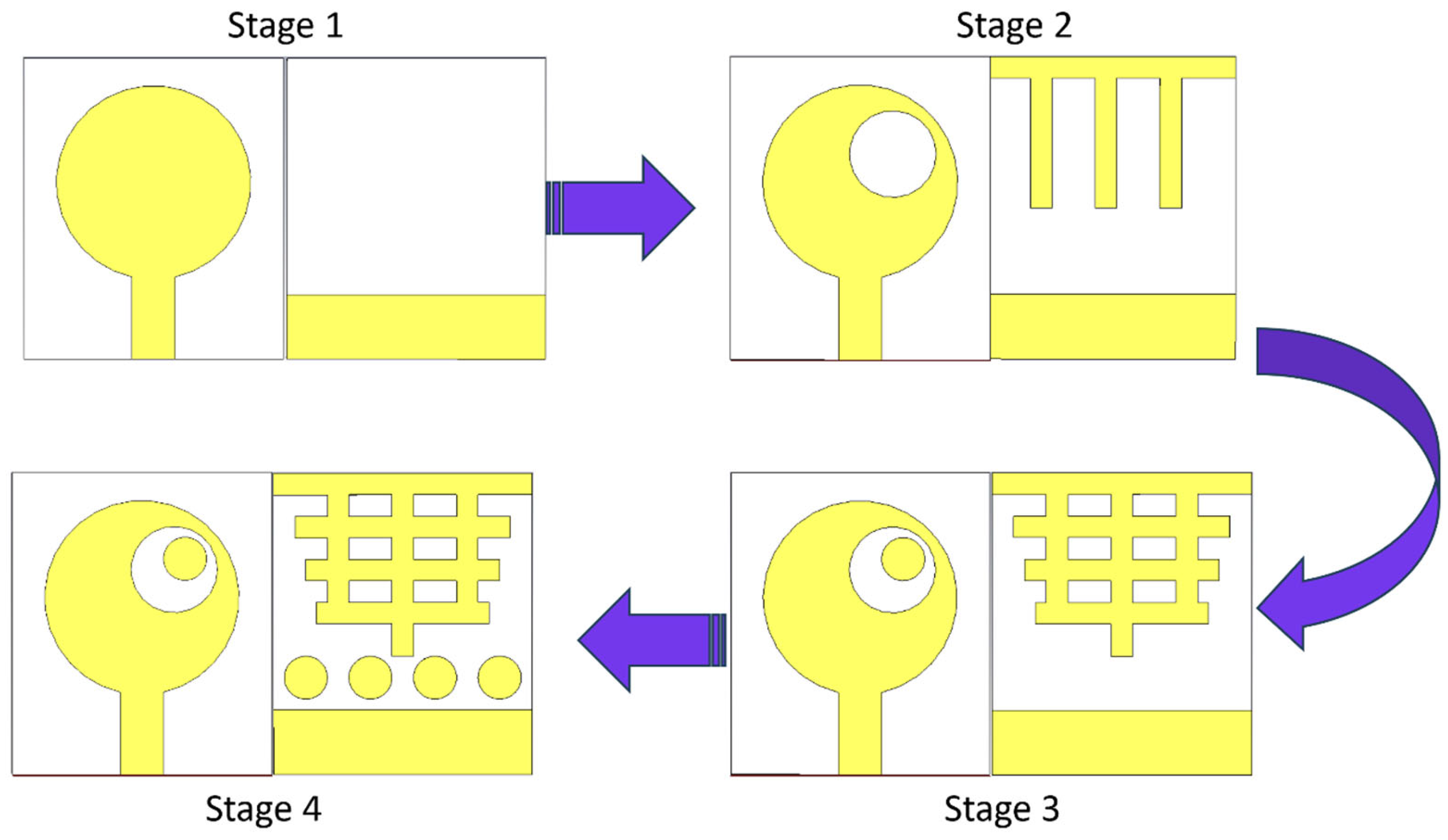
The design evolution of the proposed antenna is visually depicted in
Figure 3, illustrating the gradual development of the 5G-II band radiator. This progression is divided into four distinct phases: Step 1 initiates the process by creating a foundational circular patch along with a clearly defined ground plane radiator. In Step 2, the design advances as we introduce a circular slot into the primary patch, including a parasitic rectangular strip on the upper rear side. Step 3 involves the precise etching of a mesh structure onto the rear patch, thereby refining the antenna’s architecture through the addition of parasitic circular elements into the primary patch. Moving to Step 4, the focus is on optimizing the ground plane to attain the desired configuration. In this phase, an extra four circular elements are seamlessly incorporated on the rear side of the radiator, elevating its overall performance and resulting in the final product.
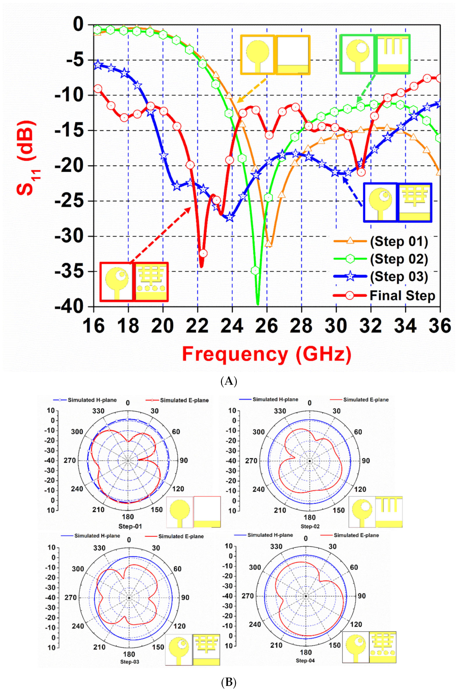
In
Figure 4A, we can observe the reflection coefficient of the proposed radiator, which signifies the magnitude of S11. These figures systematically depict the evolution of the antenna design. Beginning with Step 01, the initial configuration comprises a straightforward circular patch positioned above a stable ground plane. This circular element, measuring 9 mm in diameter, is connected through a microstrip line with dimensions of 2 mm × 4 mm. The backplane, with dimensions of 12 × 3 mm
2, gives rise to single-band resonances spanning from 23.8 to 36 GHz, as presented in
Figure 4A. A comparison of all steps in both the E-plane and H-plane is presented in
Figure 4B.
Transitioning to Step 02, a significant transformation occurs both in the front patch and on the rear side of the antenna. This modification entails reshaping the circular patch by introducing a slot in between. Consequently, the antenna’s resonance expands, creating a single-band configuration spanning frequencies from 23.5 to 36 GHz, as evident in
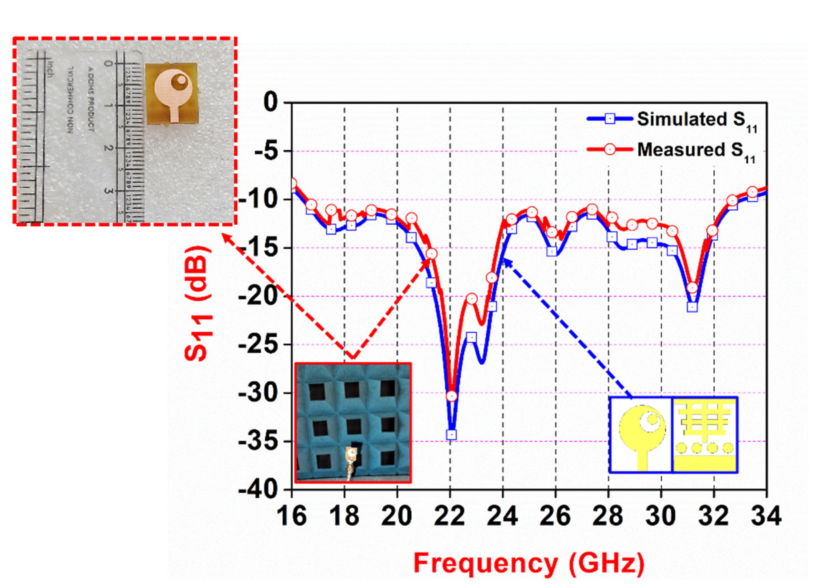
Figure 4. As we proceed to Step 03, the emphasis shifts to the rear patch, where elements of the mesh structure are etched out. These enhancements lead to improved impedance matching in the lower-order band and resonances ranging from 19 GHz to 36 GHz. In the Final Step (Step 04), a substantial modification is made to the front patch of the antenna. Four parasitic circular-shaped elements are etched out from the lower ground plane, resulting in an extended frequency range for the antenna, covering from 16.3 to 34 GHz, as depicted in
Figure 4.
5. Measurement and Simulated Results
Comprehensive measurements were conducted in an anechoic chamber to evaluate the performance of the proposed fabricated antenna. The anechoic chamber provides an isolated and controlled testing environment, minimizing external reflections and interference. A Vector Network Analyzer (VNA) was employed to measure key parameters, such as return loss, radiation patterns, and impedance characteristics. Throughout the measuring process, the antenna was accurately positioned and aligned according to the experimental setup. Multiple measurements were conducted by positioning the antenna at various angles and orientations to record its radiation patterns and assess its directional properties.
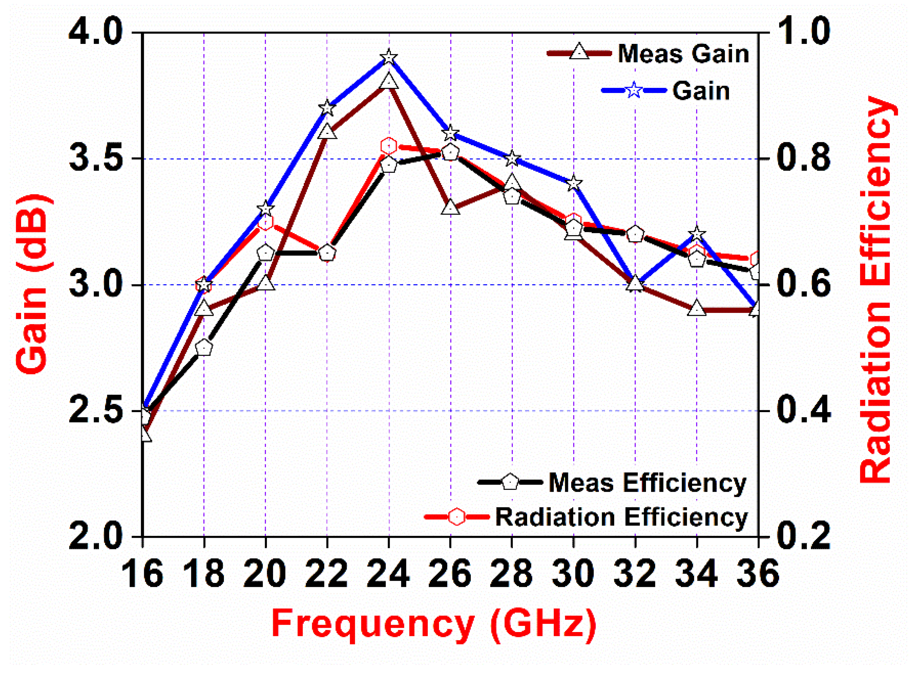
Figure 8 displays a comparison between actual measurements and simulated data from CST for our suggested antenna design. It examines the gain and radiation efficiency of the antenna across several frequencies. This comparison elucidates the performance of our antenna in real-world scenarios. An important finding from the graph is that the design achieves its peak gain, about 3.85 decibels, at the frequency where it also demonstrates its best radiation efficiency, reaching an impressive 82.9%. This correlation indicates that at this specific frequency, our antenna is producing the highest signal amplification and effectively converting a significant portion of input power into radiated energy. However, as we move to higher frequencies, an interesting trend emerges. The antenna’s electrical size decreases, resulting in an increase in ohmic losses. This, in turn, leads to a decrease in radiation efficiency at higher frequencies. This phenomenon is driven by the fact that the antenna becomes smaller relative to the wavelength at higher frequencies, causing more energy to be lost as heat due to electrical resistance. Furthermore, at these higher frequencies where the antenna’s size approaches the wavelength, we observe even higher losses due to the excitation of higher-order resonating modes. Despite these challenges, our presented antenna structure demonstrates an impressive capability to generate and reflect radiation effectively within the frequency range of 16.2 to 34 GHz. Significantly, the comparison between the measured data and the CST simulations indicates a close similarity in the plots for gain and radiation efficiency, further validating our design’s accuracy and ability to perform consistently in practical applications.
The proposed structure has undergone a comprehensive analysis to optimize its impact on the S11 parameter and other simulated outcomes. The measurement results were compared with theoretical simulations to validate the antenna’s design and verify its performance, as illustrated in
Figure 9. Deviations or discrepancies between the measurements and simulations were carefully analyzed to identify potential factors influencing the antenna’s behavior. The proposed radiator demonstrates a wide impedance bandwidth, indicating its ability to operate effectively across a range of frequencies. The bandwidth is calculated as 70.4%, covering the frequency range from 16.2 GHz to 34 GHz. This broad impedance bandwidth is crucial for accommodating multiple communication bands and ensuring efficient signal transmission. A comparison between the simulated and measured return loss validates the accuracy of the simulation model, with close agreement observed. Minor discrepancies can be attributed to fabrication tolerances and measurement uncertainties. Nonetheless, the antenna demonstrates excellent impedance matching and performs admirably within the desired frequency band.
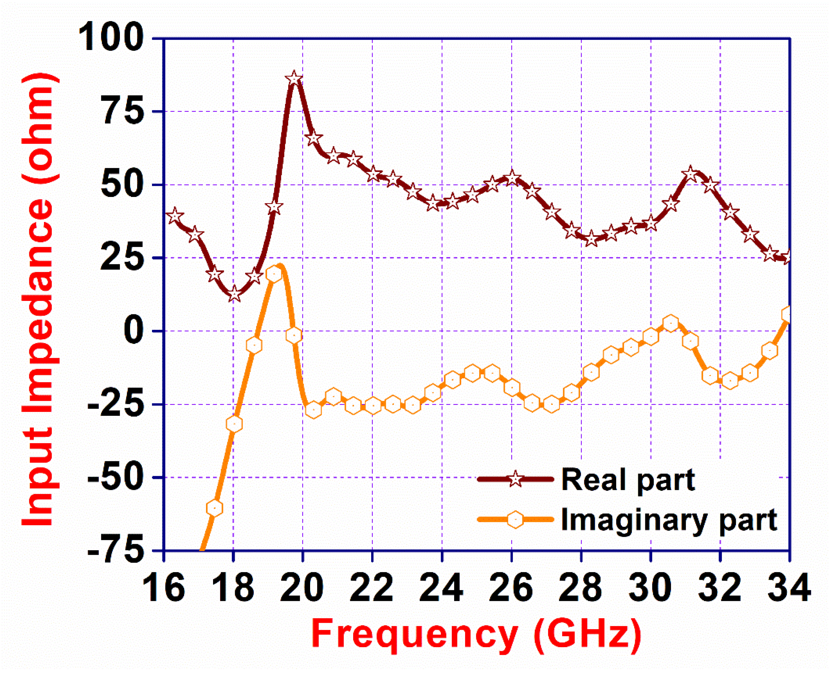
Figure 10 shows a curve representation of our proposed structure’s simulated input impedance variation. This impedance includes both the real and imaginary components, providing insights into how our design interacts with different frequencies. The curve displayed in the graph illustrates that the real component of impedance, which has been normalized to a reference value of 50 ohms, undergoes changes across the entire frequency spectrum, which spans from 16.2 to 34 GHz. Specifically, this real component ranges from 31 ohms to 69 ohms. The nature of our design’s behavior is primarily inductive within a specific frequency range, as evidenced by the positive polarity of the imaginary part of the curve between 18 and 20 GHz. Beyond this frequency range, its behavior transforms into a capacitive one, characterized by a negative polarity from 20 GHz to 30 GHz. Subsequently, the design reverts to an inductive behavior again, demonstrating characteristics that resemble both a capacitor and an inductor at higher frequencies. These impedance variations at different frequencies are crucial for understanding and optimizing the performance of our proposed structure.
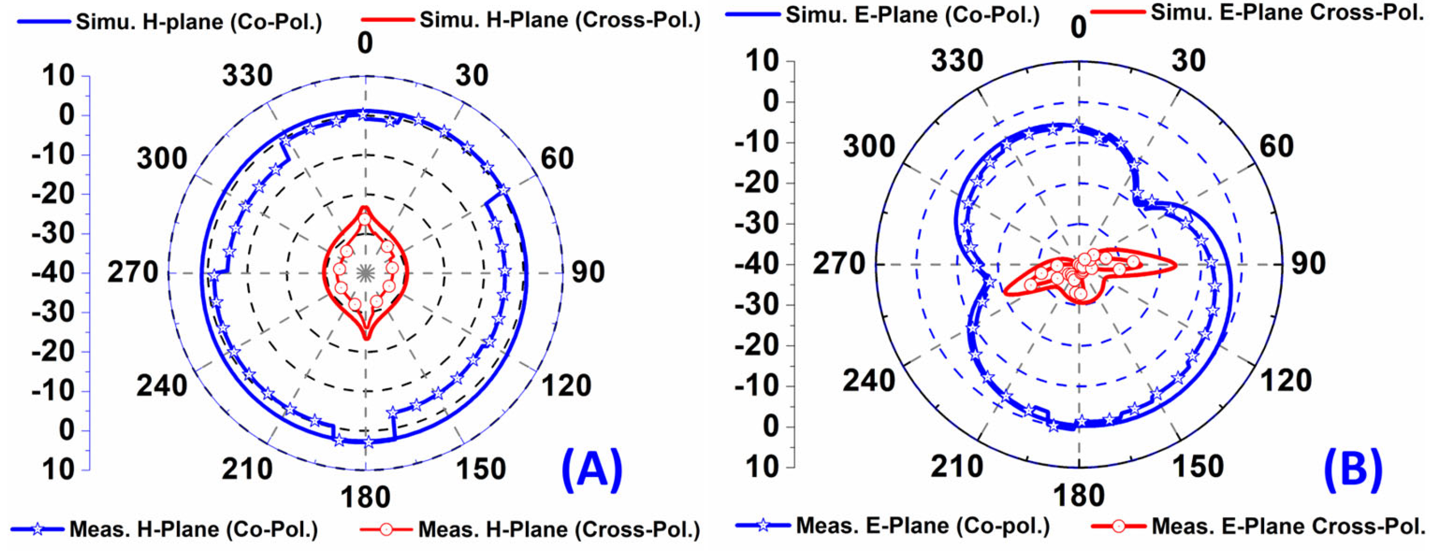
Figure 11 is an illuminating visual representation, effectively showcasing the Co (co-polarization) and Cross-polarization patterns across distinct frequencies, specifically 22 and 32 GHz. This depiction of the radiation pattern unfolds within the context of two orthogonal planes, affording a comprehensive insight into the antenna’s behavior. More precisely, the ‘E’ Plane occupies a position of 90° within the YoZ plane, while the ‘H’ Plane assumes a placement of 0° within the XoZ plane. The radiation patterns exhibit a prominent feature of being remarkably stable and consistent. The antenna’s remarkable efficiency is evident in this quality. The visualization of radiation patterns in orthogonal planes allows clear knowledge of the antenna’s directional characteristics at the selected frequencies to be obtained. The addition of both measured and simulated radiation patterns for the horizontal (H) and electric (E) planes in the illustration enhances the understanding of the topic. The consistent quality of the radiation pattern across these planes is particularly significant. The consistent behavior of the antenna acts as a strong indicator of its well-behaved and harmonious performance. The consistent and unchanging character of the antenna highlights its potential to maintain a reliable and effective performance in terms of both transmitting signals and determining direction. The intricate details of these radiation patterns are explicitly represented in
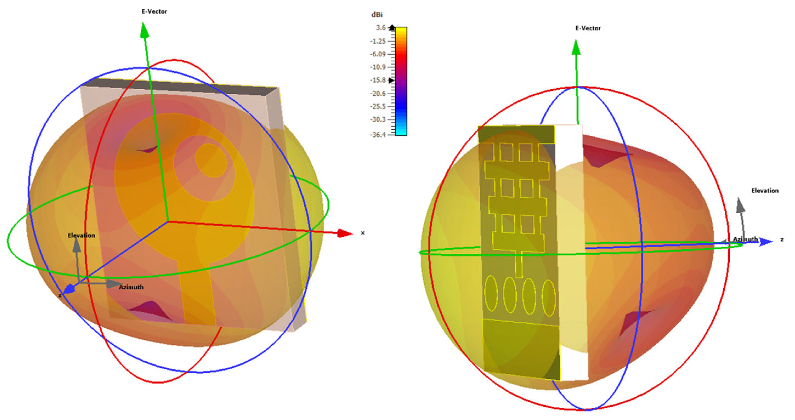
Figure 12, which provides a visualization of the antenna’s radiation patterns at the (a) 22 GHz H-plane and (b) 22 GHz E-plane.
The radiation lobe of an antenna is a crucial component that significantly influences its overall performance and operational capabilities. It plays a crucial role in explaining several elements of the antenna, such as its coverage, directionality, and emission patterns. The objective of this article is to offer an in-depth examination of the antenna’s radiation lobe, with the aim of assessing its suitability for specific use cases. In
Figure 12, we are presented with graphical representations of the antenna’s radiation patterns, known as the ‘front and rear phase lobe,’ specifically at a frequency of 22 GHz. These patterns essentially serve as a visual representation of how the antenna disperses and focuses its radiated power in distinct directions. Examining these graphs provides us with useful information about the antenna’s radiation properties when operating at the specified frequencies.
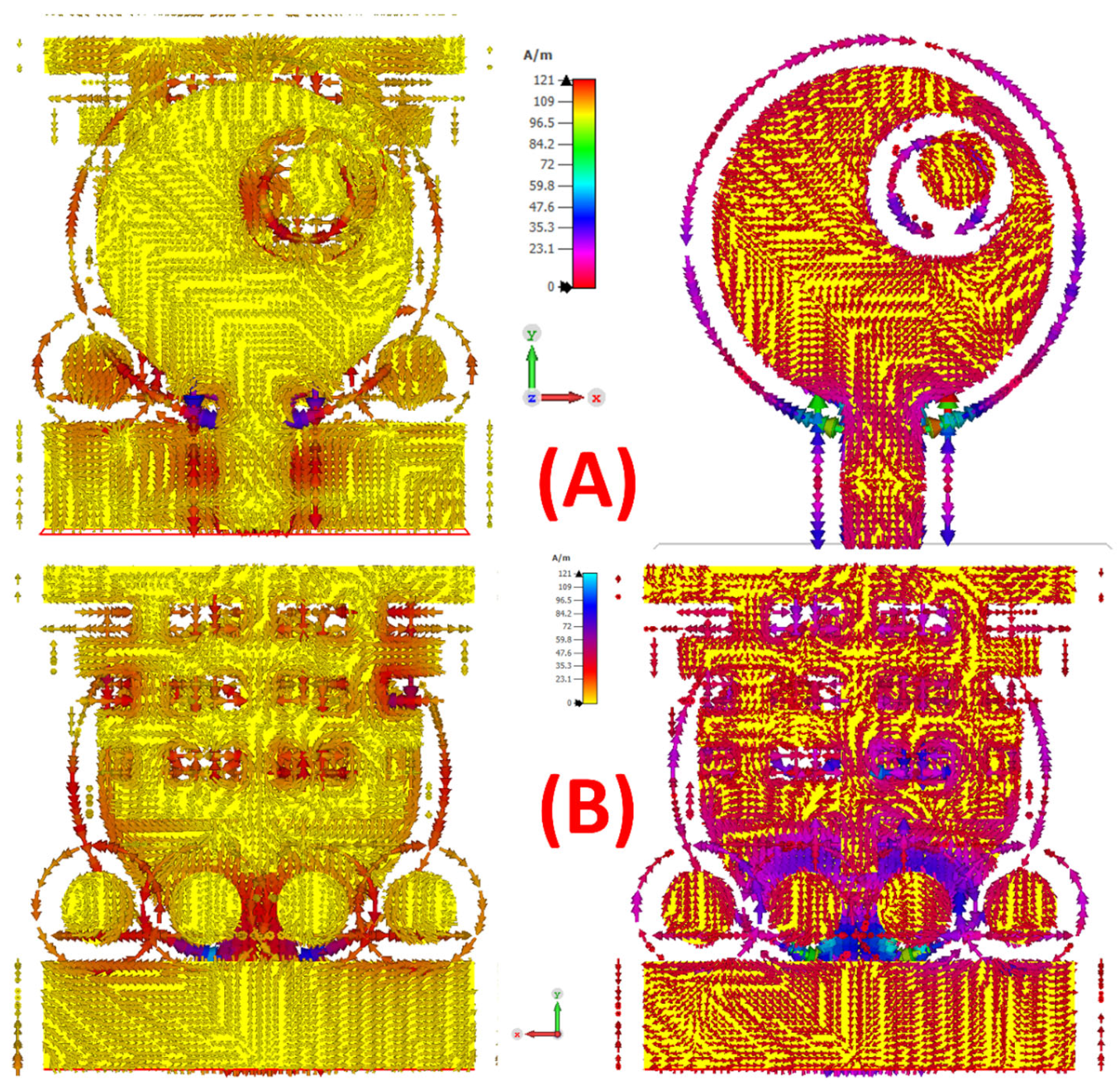
We utilized sophisticated electromagnetic simulation techniques to visually represent the surface currents of the antenna.
Figure 13 shows the antenna’s simulated surface current distribution. Color contours show current intensity, with different colors indicating current magnitude. This visualization helps identify high-current density zones and observe how currents interact with antenna sections. Analyzing front and back surface currents on the recommended antenna at 22 GHz and 32 GHz frequencies. Understanding surface current dispersion and scale helps optimize antenna configuration and uncover issues that may affect efficiency.
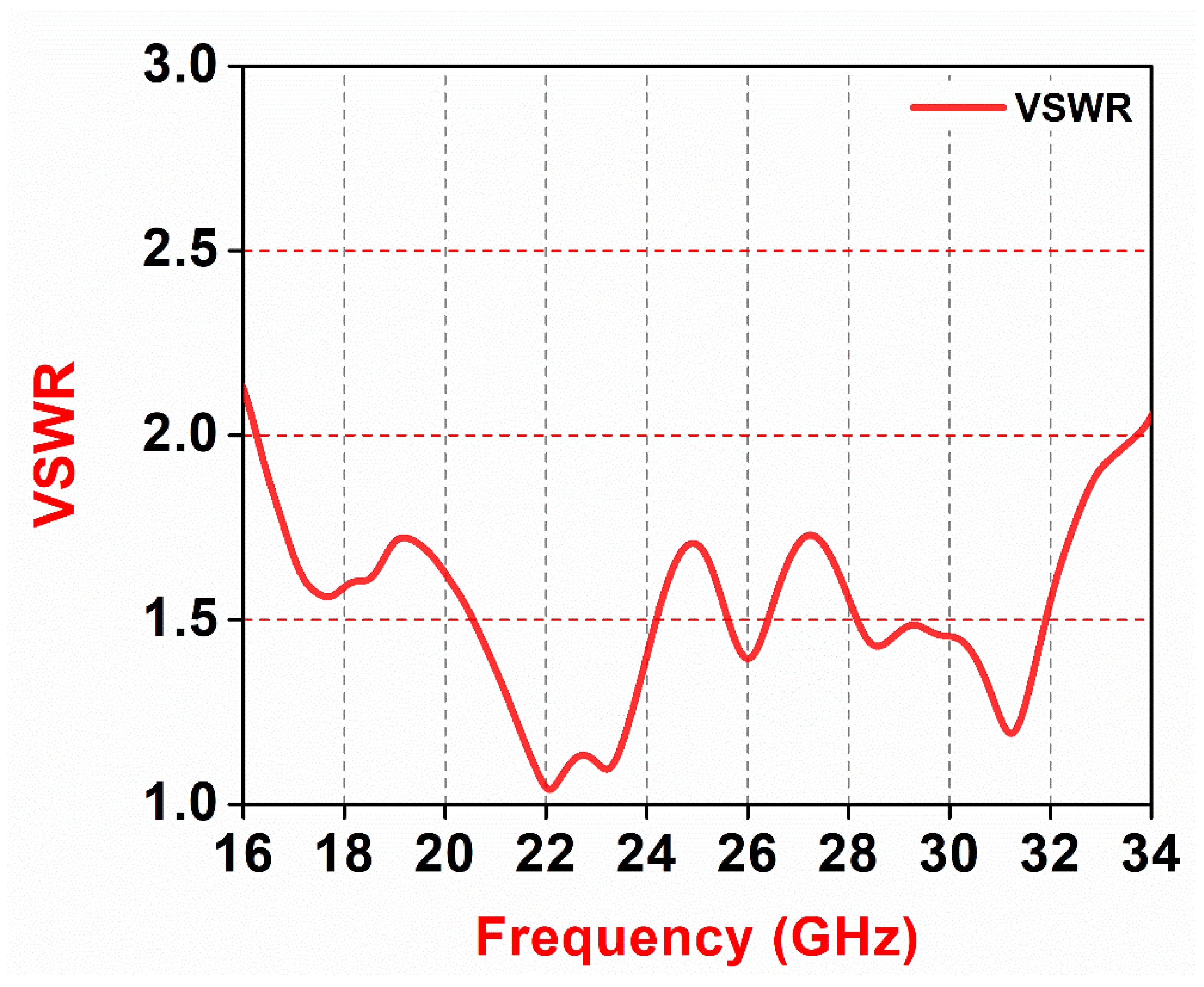
Figure 14 shows the Voltage Standing Wave Ratio (VSWR) used to test the antenna. The ratio of a transmission line’s highest to lowest voltage is VSWR, an important antenna engineering metric. A decrease in VSWR indicates better impedance matching, leading to higher antenna efficiency. The graph in
Figure 14 illustrates the VSWR characteristics of the analyzed antenna, providing information on its power transfer efficiency to the transmission line and the presence of reflections. A well-designed antenna typically exhibits a consistently low VSWR across its operational frequency range.
The results presented in
Figure 14 validate the antenna’s design and shed light on its impedance-matching capabilities. This analysis contributes to a comprehensive understanding of the antenna’s behavior, ensuring its suitability for practical communication applications. The VSWR assessment is a fundamental step in confirming the antenna’s effectiveness, aligning with industry standards and critical to evaluating overall antenna performance.
Table 1 demonstrates a contrast between antennas that have been previously documented. After evaluating multiple parameters, it has been established through our analysis that the design we propose is smaller in dimension and displays enhanced characteristics compared to the antennas previously documented.
