Article

A High Step-Down SiC-Based T-Type LLC Resonant Converter for Spacecraft Power Processing Unit

School of Aeronautics and Astronautics, University of Electronic Science and Technology of China, Chengdu 611731, China
*
Author to whom correspondence should be addressed.
Aerospace 2024, 11(5), 396; https://doi.org/10.3390/aerospace11050396
Submission received: 31 March 2024 / Revised: 9 May 2024 / Accepted: 12 May 2024 / Published: 15 May 2024
(This article belongs to the Special Issue Advanced Chemical Propulsion and Electric Propulsion)

Abstract

:
A spacecraft power processing unit (PPU) is utilized to convert power from solar arrays or electric batteries to the payload, including electric propulsion, communication equipment, and scientific instruments. Currently, a high-voltage converter is widely applied to the spacecraft PPU to improve power density and save launch weight. However, the high voltage level poses challenges such as high step-down ratios and high power losses. To achieve less conduction loss, a SiC-based T-type three-level (TL) L L C resonant converter is proposed. To further broaden the gain range and achieve high step-down ratios, a variable frequency and adjustable phase-shift (VFAPS) modulation scheme is proposed. Meanwhile, the steady-state time-domain model is established to elaborate the operation principles and boundary conditions for soft switching. Furthermore, the optimal resonant element design considerations have been elaborated to achieve wider gain range and facilitate easier soft switching. Furthermore, the numerical solutions for switching frequency and phase shift (PS) angle under each specific input could be figured out. Finally, the effectiveness of this theoretical analysis is demonstrated via a 500-W experimental prototype with 650∼950-V input and constant output of 48-V/11-A.

1. Introduction

The power processing unit (PPU) serves as the core of a spacecraft power system. As is shown in Figure 1, it is responsible for managing and distributing power generated by solar arrays or nuclear reactors to the payload, including electric propulsion, communication equipment, and scientific instruments [1,2,3]. High-voltage (500∼1500 V) PPUs are widely adopted, for it could effectively satisfy different DC loads, reduce conduction losses, and save launch weight. However, this poses a series of challenges to the converter, such as high step-down ratios and severe power losses.
(1) The intermittency of solar energy will lead to bus voltage fluctuation in the PPU, which requires high efficiency over a wide input range and narrow modulated frequency variation [4].
(2) The voltage level of communication equipment and scientific instruments are generally between 21 and 48 V, which requires high step-down conversion. This would induce small duty cycles for the switches, leading to frequent transitions, high voltage overshoot, and severe EMI [5].
To achieve higher efficiency, soft-switching topologies are prioritized over hard-switching due to its minimized switching losses. A 50-kW phase-shift full-bridge (PSFB) converter is proposed in [6] for electric vehicle (EV) ultra-fast charging (XFC) applications. Through modulating the phase shift (PS) angle, it could regulate the power transferred and produce resonant energy for switches. However, PSFB could hardly achieve zero voltage switching (ZVS) for the lagging-leg switches in light load conditions. Compared with PSFB, a series resonant converter (SRC) shows better soft-switching performance. A bidirectional charge-controlled SRC is proposed in [7] to achieve direct control of the charge flow and minimized reactive power loss. However, SRC could only broaden its gain range in the buck region. Regarding this, a 3-kW SRC buck-boost converter, achieving a wide gain range (800 V to 200∼950 V) and all switches ZVS, is proposed in [8] for an EV charger. By employing frequency or PS modulation, the converter could switch between the buck or boost modes, whereas parasitic resistances induced by the large magnetizing inductance will lead to high core loss. More importantly, the gain voltage of SRC cannot be adjusted in short-circuited conditions. Compared with SRC, the parallel resonant converter (PRC) shows better performance in gain voltage regulation and could effectively protect against short circuits. A constant-current input PRC is proposed in [9] for long-distance power distribution, whose output could be flexibly regulated over a wide load range. However, PRC exhibits high turn-off losses and reactive losses under a high input voltage. Compared with these two-element (SRC, PRC) topologies, the emergence of three-element resonant converters, for instance L C C , C L L , and L L C , could effectively improve the aforementioned problems. A current-fed L C C converter is proposed in [10] to transfer 30∼42-V input to 380-V output for photovoltaic/fuel cell applications. Due to the paralleled bulky capacitances, L C C shows better performance in low input and high output applications, but it is not suitable for wide load regulation. Regarding this, L L C shows better performance. In [11], a PWM-modulated L L C is proposed for power takeoff systems, which could achieve high gain and soft switching over a wide input and load range. In [12], a novel PWM-modulated L L C with a modified voltage doubler is proposed for the onboard charger (OBC), which could transfer 390-V input to 250∼420-V output with the peak efficiency of 96.7%. C L L shows similar behavior as in L L C [13,14], whereas it integrates the leakage inductance to the secondary side, which doubles the secondary-side conduction loss and decreases the design precision of leakage inductance. There are also four or more elements utilized in resonant converters, like L C L C [15,16], L C L C L [17], and L C 2 L C 2 [18]. These multi-element resonant converters could inject less harmonics into the output, thus lowering the conduction loss and EMI level. However, adding more elements will lead to greater circuit complexity and energy losses. The pros and cons of the resonant converters are summarized in Table 1. Considering the overall aspects, L L C could be a promising candidate to balance the gain range and efficiency for PPU applications.
The spacecraft PPU is tasked with converting high voltage (HV) generated by solar arrays into a low voltage (LV) suitable for scientific instruments. Such high step-down ratios necessitate switches operating at small duty cycles, making soft switching hard to achieve. To solve this problem, two ways are developed: one is adopting wide bandgap (WBG) semiconductor devices with small output junction capacitance, such as silicon carbide (SiC)-type or gallium nitride (GaN)-type devices [19,20]; the other is using multi-level topology to reduce the switching voltage drop. Compared with silicon (Si) devices, SiC and GaN exhibit higher electron mobility and electron saturation velocity, enabling them to operate at higher frequency. Moreover, SiC demonstrates superior thermal conductivity than GaN or Si, rendering it more suitable for high-power applications. In [21], a 15-kW SiC-based PPU for a Hall thruster is presented, whose peak efficiency could reach 97% under full load conditions. The multi-level topologies could effectively reduce the voltage drop on each switch, thereby allowing for easier soft switching, less voltage/current stress on switches, and lower total harmonic distortion (THD). Neutral point clamped (NPC), as the representative multi-level topology, exhibits a simple structure and good dynamic response [22]. However, NPC needs freewheeling diodes and has an issue of an uneven DC-link voltage, which requires additional balancing circuits or a complex control strategy. To improve this, a novel NPC-based voltage balancing strategy is proposed in [23] for traction application. To further simplify the circuit and minimize components, a four-level nested NPC (NNPC) is proposed in [24], which could achieve a very wide gain range and low voltage stress. In [25], an asymmetrical cascaded H-bridge (CHB) is proposed to reach high power levels and high reliability at the advantage of its modular and fault-tolerant features, whereas CHB requires isolated DC links, which is not suitable for PPU. In [26], a comparison between a modular multilevel converter (MMC) and NPC is proposed in the medium-voltage application. It is concluded that MMC performs more balanced power losses and less harmonics due to its scalable structure. However, MMC requires large number of bulky capacitances and precharging process, which are not applicable on spacecraft. Full-bridge (FB) could be applied to multi-level use as well [27,28]. With the same input and output ranges, its conducting current is only half that of NPC, leading to smaller current stress and less conduction loss, whereas its doubling resonant tank input voltage will bring challenges to the transformer insulation and withstand voltage. Although these multi-level topologies effectively lower the voltage or current stress, they always have more than two switches carrying the same conducting current simultaneously, which achieves the lower voltage stress at the expense of higher conduction loss. Compared with these topologies, T-type exhibits only one switch that produces conduction loss in positive or negative input [29]. Moreover, compared with FB, the T-type could effectively reduce insulation levels of the transformer and the voltage stress on half of switches. Consequently, the adoption of SiC device and T-type are more suitable for high-step down applications.
In this paper, a SiC-based T-type L L C resonant converter will be presented for the spacecraft PPU. Due to the asymmetry of T-type, low voltage stress and low turn-off current are imposed on the auxiliary leg. More importantly, there will be only one switch that produces conduction loss in positive or negative input, thus improving the overall efficiency. To achieve a wider gain range and high step-down ratios, a variable frequency and adjustable phase-shift (VFAPS) modulation scheme is proposed. The operation modes, boundary conditions for VFAPS scheme, are expounded in detail via a time-domain analysis. The numerical solutions for parameter settings of VFAPS are figured out. Moreover, resonant element consideration for easier soft switching are given for design guidance. Finally, the effectiveness of this theoretical analysis is verified via a 500-W prototype with 650∼950-V input and constant 48-V/11-A output, whose peak efficiency is able to reach 96.81% under full load conditions.

2. The Topology and Operation Modes

2.1. The Topology

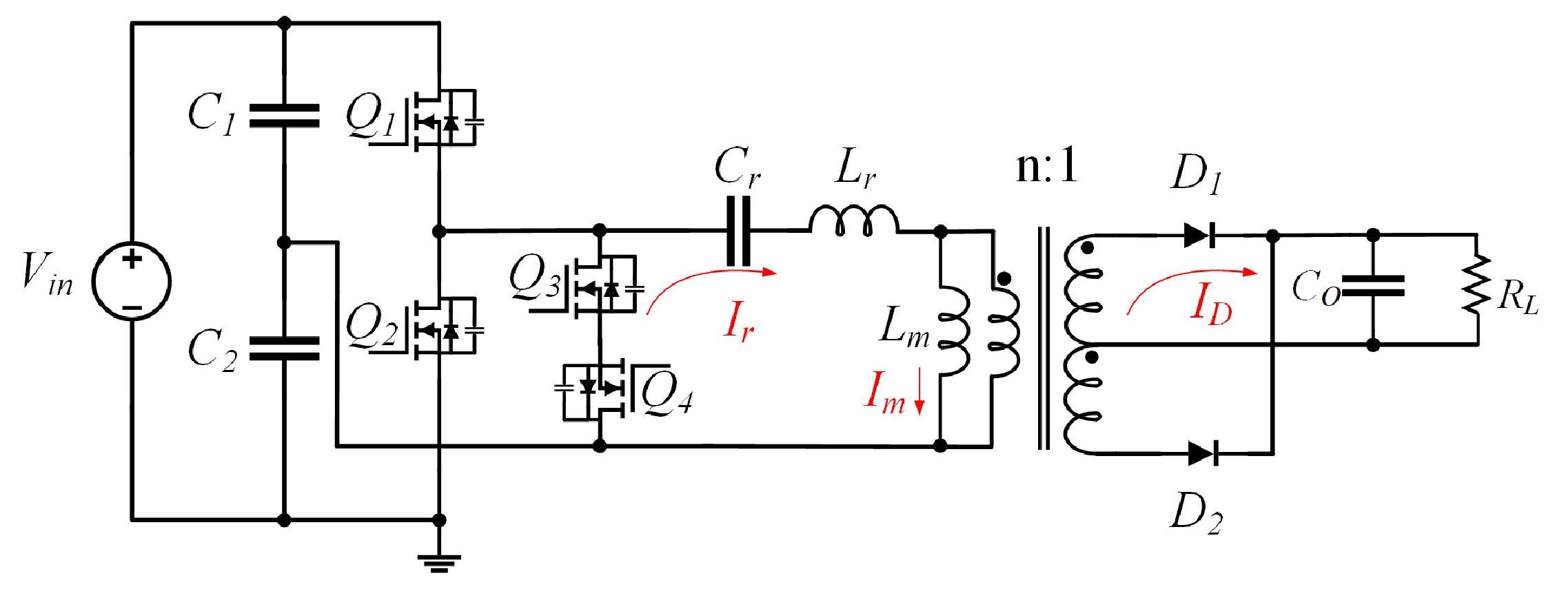
As Figure 2 shows, we adopt T-type for high step-down usage. It additionally has two MOSFETs Q 3 , Q 4 attached and two split input capacitors C 1 , C 2 to a conventional half-bridge (HB) composed of Q 1 , Q 2 . Q 3 , Q 4 are in series sharing the same source and are connected in parallel with the resonant tank. C 1 , C 2 adopt the same large capacitance, which could both stabilize their voltage at half of input V i n 2 . The resonant inductance L r , magnetizing inductance L m , and resonant capacitor C r together constitute the resonant tank, with one end a connected to the midpoint of HB and the other b to the midpoint of the split capacitors. The voltage difference between points b, a V b a , which is also the input voltage of resonant tank, transforms among V i n 2 , 0, V i n 2 . I r and I m represent the resonant and magnetizing current, respectively. V C r represents the voltage across C r . V D S , V G S indicate the voltage across the DS and GS of the switch, respectively. V D indicates the voltage across the diodes D 1 , D 2 on the secondary side. I D indicates the current flowing through D 1 , D 2 . C o s s indicates the junction capacitance of switches. R L is the output DC resistance.
The switching waveforms of four driving switches Q 1 , Q 2 , Q 3 , Q 4 are shown as the blue shadow area in Figure 3. The dotted line has divided the waveforms into different stages, which are detailedly elaborated in 2.2. Ignoring the dead times, Q 1 , Q 3 and Q 2 , Q 4 are two pairs of complementary driving signals.
f r 1 = 1 2 π L r C r
w r 1 = 2 π f r 1
L p = L r + L m
f r 2 = 1 2 π L p C r
w r 2 = 2 π f r 2
where f r 1 is the resonant frequency when both L r and C r participate in resonance, and f r 2 indicates the resonant frequency when L r , L m , and C r are all in resonance. w r 1 , w r 2 are the radians of f r 1 , f r 2 , respectively.

2.2. The Operation Modes

This subsection will elaborate several operation modes modulated by the VFAPS scheme. As is shown in Figure 3b,c, the overlap between the signals of Q 3 , Q 4 is defined as the PS angle φ , which is utilized to regulate the voltage gain. With different switching frequency f s and φ , the operation modes are totally distinctive.
(1) HB Mode: As Figure 3a shows, if only the traditional frequency modulation (FM) scheme is utilized, both Q 1 and Q 2 operate with a duty ratio of 50%. T-type makes no difference from the HB L L C , whose gain range is fairly limited in heavy load conditions.
(2) Mode 1: As Figure 3b shows, Mode 1 indicates the situation that V b a drops to zero after I r ( t ) meets I m ( t ) . Mode 1 only operates in the condition that f s ( f r 2 , f r 1 ), φ ∈ [0, w r 2 t x ]; here, t x indicates the time when I r and I m meet, and T s indicates the switching period. Since the gain in Mode 1 is adjusted by modulating the proportion of reactive current, its gain range is fairly limited as well.
(3) Mode 2: As Figure 3c shows, Mode 2 indicates the situation that I r ( t ) has not met I m ( t ) by the time V b a turns to zero. f s in Mode 2 can operate among f r 2 < f s < f r 1 , f s = f r 1 , f s > f r 1 . When f r 2 < f s < f r 1 , φ ∈ ( w r 2 t x , w r 2 t x + w r 1 ( T s 2 t x ) ). In addition, when f s f r 1 , Mode 2 will be maintained if φ > 0 . As the gain in Mode 2 could be adjusted by modulating the proportion of active current I r I m , its gain range is much wider than the former two.

2.3. The Time-Domain Analysis of Mode 2

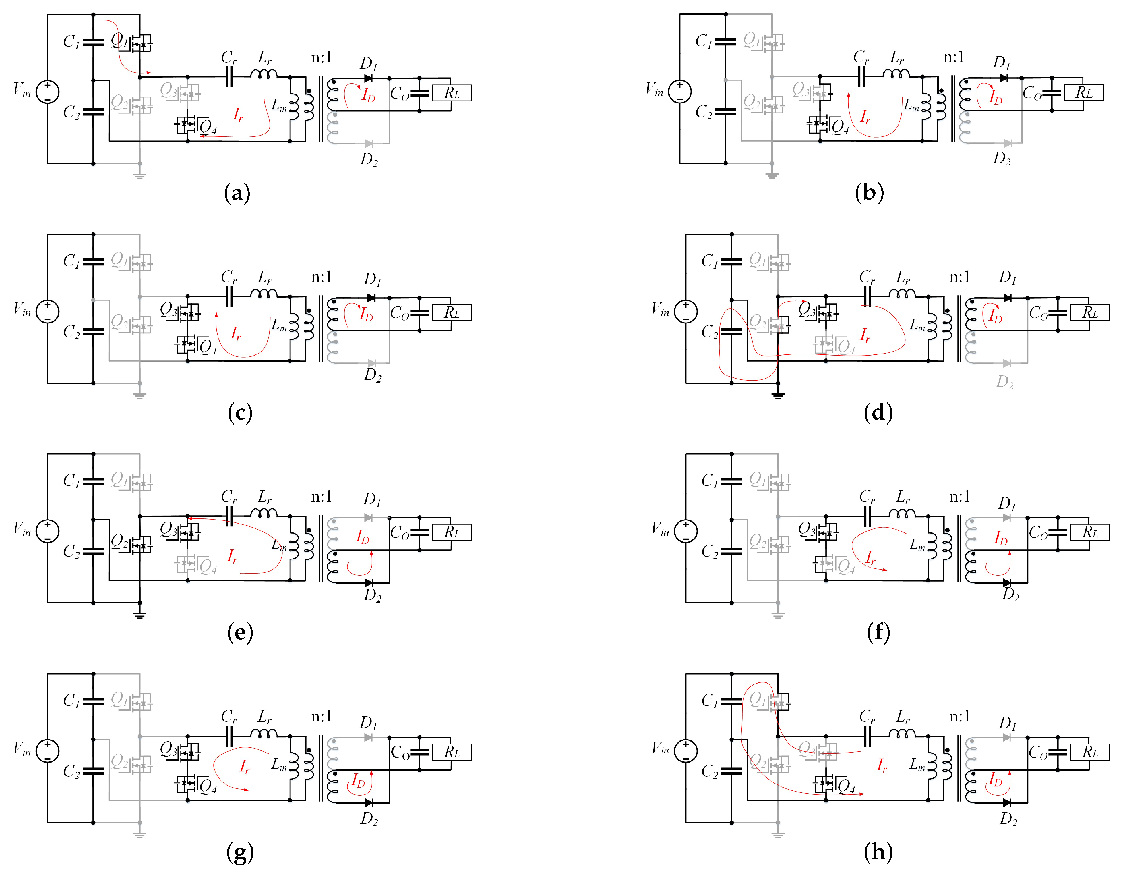
The equivalent circuits of Mode 2 in different stages are shown in Figure 4. Only circuits in the positive direction will be discussed here.
Stage 1 [ t 0 , t 1 ]: As Figure 4a shows, Q 1 , Q 4 are on, and V b a = V i n / 2 . I r flows in the positive direction as a sinewave with the resonant frequency of f r 1 . As Q 3 is off, there will be no current flowing through the auxiliary leg. Since the voltage across L m is clamped by the output V o , I m changes linearly with the ratio of n V o / L m . As for the secondary side, D 1 automatically starts to conduct at t 0 . Only Q 1 and D 1 suffer conduction loss. The time-domain equations are as follows:
L r C r d V c r 2 d t 2 + V c r + n V o = V i n 2 ,
V c r ( t ) = V i n 2 n V o + V c r ( t 0 ) V i n 2 + n V o cos w r 1 t + L r C r I r ( t 0 ) sin w r 1 t ,
I r ( t ) = C r w r 1 V c r ( t 0 ) V i n 2 + n V o sin w r 1 t + L r C r I r ( t 0 ) cos w r 1 t .
L m d I m d t = n V o I m ( t 1 ) I m ( t 0 ) = n V o L m t 1 .
Stage 2 [ t 1 , t 2 ]: As Figure 4b shows, Q 4 is on, and V b a = 0 . Q 1 is turned off, so that V D S 1 will be charged from 0 to V i n / 2 , and V D S 2 will be discharged from V i n to V i n / 2 . I r ( t ) freewheels through the auxiliary leg, thus discharging V D S 3 from V i n / 2 to 0. The equivalent junction capacitance C p a r for energy commutation is C o s s 1 + C o s s 2 + C o s s 3 within this stage. As the flux linkage between the primary and secondary side has not vanished, I m ( t ) keeps increasing linearly. D 1 keeps conducting to convert energy to V o . This stage will end when C o s s 3 finishes discharging. In this stage, Q 1 suffers hard turn-off loss, the magtitude of which is relevant to the I r ( t 1 ) . Q 4 and D 1 suffer conduction loss. Since C o s s 3 has not been totally discharged within this interval, Q 3 will not suffer any loss. The time-domain equations are as (10) shows.
Stage 3(a) [ t 2 , t 3 ]: As Figure 4c shows, Q 3 , Q 4 are on, and V b a = 0 . Q 3 is turned on as ZVS. I r ( t ) will remain in the positive direction and flows through the auxiliary leg. I m ( t ) is increasing linearly as with the previous two stages. At t 3 , when I r ( t ) meets I m ( t ) , the flux linkage between primary and secondary side has finally exhausted, and therefore, the voltage across L m is no longer clamped by V o and only depends on the ratio of d I m ( t ) / d t afterwards. As for the secondary side, since V D 1 decreases from positive to V o at t 3 , D 1 will suffer a little reverse recovery loss, whose magnitude depends on the slope ratio of I D ( t 3 ) . However, compared with FM when f s > f r 1 , the reverse recovery loss under VFAPS is much reduced. L r , C r , L m will start to participate in resonance in the next stage. In this stage, Q 3 , Q 4 , D 1 suffer conduction loss. The time-domain equations are as follows:
L r C r d V c r 2 d t 2 + V c r + n V o = 0 ,
V c r ( t ) = n V o + ( V c r ( t 1 ) + n V o ) cos w r 1 t + L r C r I r ( t 1 ) sin w r 1 t ,
I r ( t ) = C r w r 1 ( V c r ( t 1 ) + n V o ) sin w r 1 t + L r C r I r ( t 1 ) cos w r 1 t ,
L m d I m d t = n V o I m ( t 3 ) I m ( t 0 ) = n V o L m t 3 .
According to the law of conservation of energy, the input energy of the resonant tank should be equal to the output energy, which can be given by
E p e r c y c l e = V b a I r ( t ) d t = V o 2 R L f s
where V b a will remain at V i n 2 from t 0 to t 1 , and zero from t 1 to t 3 . Thus, (14) can be re-written as
V i n 2 C r V C r ( t 1 ) V C r ( t 0 ) = V o 2 2 R L f s .
Stage 3(b) [ t 3 , t 4 ]: As Figure 4c shows, Q 3 , Q 4 are on, V b a = 0 . I r ( t ) meets I m ( t ) at t 3 , and they flow together in the resonant frequency of f r 2 . Since the voltage across L m is no longer clamped by V o , both D 1 and D 2 are unable to conduct. C o plays as a voltage source to feed the load. If this stage lasts for too long to make I r ( t 4 ) turn negative, there will be no energy discharging C o s s 2 , so that Q 2 could not achieve ZVS in the next stage. This stage will end when I r ( t 4 ) is still positive and has enough energy to discharge C o s s 2 . In this stage, Q 3 , Q 4 suffer conduction loss. The time-domain equations are as Equation (10) show.
Stage 4 [ t 4 , t 5 ]: As Figure 4d shows, Q 3 is on, and V b a = 0 . Q 4 is turned off at t 4 , V D S 4 will be charged from 0 to V i n / 2 . The residual positive I r ( t ) will help discharge C o s s 2 , so that V D S 2 will be discharged from V i n / 2 to 0, and V D S 1 will be charged from V i n / 2 to V i n . C p a r for energy commutation is C o s s 1 + C o s s 2 + C o s s 4 . This stage will end when V D S 2 = 0 . In this stage, Q 4 is turned off at a very small current I r ( t 4 ) , and thus, the hard turn-off loss is generally negligible. Q 3 suffers conduction loss. The time-domain equations are as follows:
L p C r d V c r 2 d t 2 + V c r = 0 ,
V c r ( t ) = V c r ( t 0 ) cos ( w r 2 t ) L p C r I r ( t 0 ) sin ( w r 2 t ) ,
I r ( t ) = C r w r 2 V c r ( t 0 ) sin ( w r 2 t ) L p C r I r ( t 0 ) cos ( w r 2 t ) .

3. The Design Algorithm

Through a time domain analysis, this section will provide guidance for the proposed VFAPS modulation scheme and L L C design considerations. We aim to figure out the numerical solutions for f s and φ and the optimal parameters for resonant elements with requirement of a specified range of V i n . First, the basic parameters used in derivations are listed in Section 3.1. Second, boundary conditions for f s and φ to obtain soft switching under the minimum input voltage V i n m i n and maximum input voltage V i n m a x are given in Section 3.2. Moreover, the design considerations for the resonant elements are given in Section 3.3. Finally, according to the boundary conditions, the numerical algorithm to calculate the solutions for f s and φ under each specified V i n are given in Section 3.4.

3.1. Basic Parameters Used in Derivations

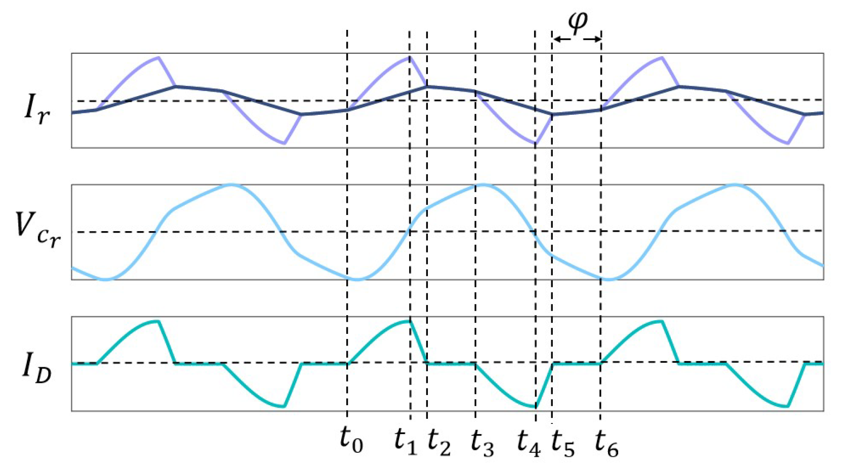
The basic variables used in time-domain derivations are defined here. As Figure 5 shows, the time durations divded by the dotted line ( t 1 t 0 , t 2 t 1 , t 3 t 2 ) in terms of radian ( α , β , γ ) are listed as follows:
α = w r 1 ( t 1 t 0 ) = w r 1 T s 2 β w r 1 γ w r 2 ,
β = w r 1 ( t 2 t 1 ) = w r 1 T s 2 α w r 1 γ w r 2 ,
γ = w r 2 ( t 3 t 2 ) = w r 2 T s 2 α + β w r 1 .
Therefore, φ can be expressed as
φ = β + γ .
The steady-state equations at t 2 can be expressed as follows by substituting (7) and (8) into (11)–(13):
V C r ( t 2 ) = V C r ( t 0 ) V i n 2 + n V o cos ( α + β ) + L r C r I r ( t 0 ) sin ( α + β ) n V o + V i n 2 cos β ,
I r ( t 2 ) = C r w r 1 V i n 2 sin β + L r C r I r ( t 0 ) cos ( α + β ) V C r ( t 0 ) V i n 2 + n V o sin ( α + β ) ,
I m ( t 2 ) = n V o L m t 2 + I m ( t 0 ) .
The steady-state equations at t 2 can also be deduced from (17) and (18) as follows:
V C r ( t 2 + ) = V C r ( t 0 ) cos γ + L p C r I r ( t 0 ) sin γ ,
I r ( t 2 + ) = I m ( t 2 + ) = C r w r 2 V C r ( t 0 ) sin γ L p C r I r ( t 0 ) cos γ .

3.2. Boundary Conditions

This section will utilize the limiting soft-switching conditions and the boundaries between Mode 1 and 2 to deduce the boundary ranges for f s and φ . These ranges are used for the resonant elements design and numerical solutions of VFAPS modulation under the specified V i n range.

3.2.1. Boundary Conditions for Soft Switching

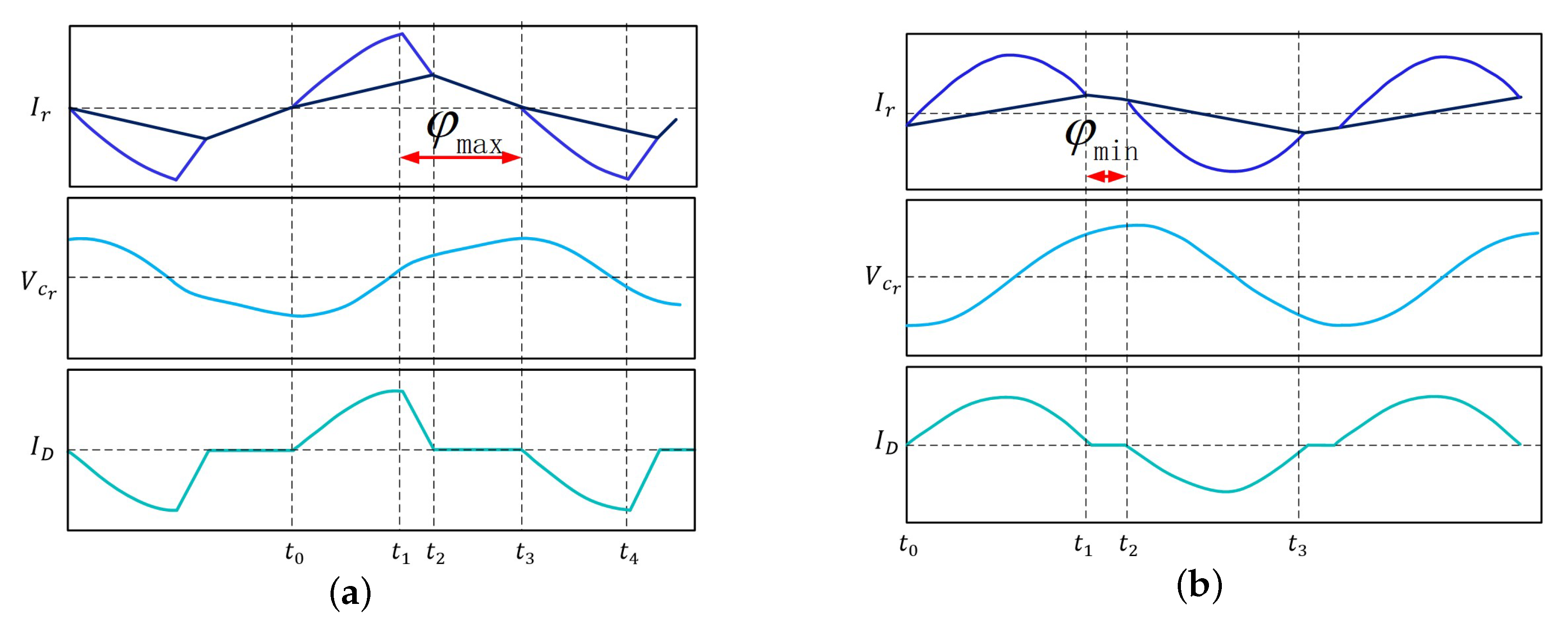
Since V i n will increase with the increment of φ to sustain the stable V o , there is supposed to be a maximum PS angle φ m a x to ensure that all switches are soft switching under each specified f s . According to FM and operation modes in Section 2.3, this limiting soft-switching condition corresponds to V i n m a x , the minimum switching frequency f s m i n , and φ m a x .
Figure 6a shows the steady-state waveforms under this limiting soft-switching condition. Specifically, to obtain the V i n m a x under f s m i n , φ should be set as large as possible. However, if φ is too large to make the I r ( t 3 ) turn from positive to negative, there will be no current discharging C o s s 2 , and ZVS of Q 2 will not be achieved in the next stage. That is to say, zero is the threshold for I r ( t 3 ) to both ensure the ZVS of switches and the V i n m a x under f s m i n .
Due to the symmetry of waveforms, it can be listed that
I r ( t 0 ) = I r ( t 3 ) = 0 .
Taking (28) into (23)–(26), two planes f 1 , f 2 composed only of f s m i n and γ are listed as follows. Since the equations are both nonlinear, the analytical solutions are hard to obtain. Here, we utilize the Binary Numerical Iteration method to obtain numerical solutions for f s m i n and γ , so that φ m a x could be further deduced. The detailed solving steps are illustrated in Section 3.4.
f 1 ( f s m i n , γ ) = n V o + V i n m a x 2 cos ( w r 1 ( 1 2 f s m i n arccos V o 2 R L f s m i n V i n m a x C r L p C r n V o 1 2 f s m i n γ w r 2 L m sin γ + n V o V i n m a x 2 + 1 w r 1 γ w r 2 ) ) + n V o V i n 2 cos w r 1 1 2 f s m i n γ w r 2 L p C r n V o 1 2 f s m i n γ w r 2 L m sin γ cos w r 1 1 2 f s m i n γ w r 2 + cos γ = 0 ,
f 2 ( f s m i n , γ ) = V i n m a x 2 sin w r 1 1 2 f s m i n arccos V o 2 R L f s m i n V i n m a x C r L p C r n V o 1 2 f s m i n γ w r 2 L m sin γ + n V o V i n m a x 2 + 1 w r 1 γ w r 2 ( n V o V i n 2 ) sin w r 1 1 2 f s m i n γ w r 2 L p C r n V o ( 1 2 f s m i n γ w r 2 ) L m sin γ L r L p sin γ sin w r 1 1 2 f s m i n γ w r 2 = 0 .

3.2.2. Boundary Conditions between Mode 1 and Mode 2

Mode 1 occurs when f s < f r 1 and φ [0, w r 2 t x ]. Compared with Mode 2, the gain range of Mode 1 is much narrower, and its I m ( t ) is comparatively larger, which will unnecessarily increase the conduction loss and reactive power loss, and therefore, Mode 1 will not be the focus in this paper. However, in order to figure out the realizable region of Mode 2 when f s < f r 1 , the boundary conditions between Mode 1 and Mode 2 should be made clear.
Figure 6b shows the steady-state waveforms of the boundary condition between Mode 1 and Mode 2. Specifically, the φ is set as w r 2 t x here, which could turn off the V b a by the time that I r ( t ) meets I m ( t ) . Since V i n increases with the increment in φ under a specified f s , when f r 2 < f s < f r 1 , this boundary condition corresponds to V i n m i n , f s m a x , and the minimum PS angle φ m i n . As Figure 6b shows, Stage 3(a) is entirely absent. According to the continuity of the waveform, we combine (13), (15), (26) and (27), and the time-domain equations at t 1 can be expressed as follows:
V c r ( t 1 ) = V c r ( t 1 + ) n V o + V i n m i n 2 + V c r ( t 0 ) V i n m i n 2 + n V o cos α + L r C r I r ( t 0 ) sin α = V c r ( t 0 ) cos γ + L p C r I r ( t 0 ) sin γ ,
I r ( t 1 ) = I r ( t 1 + ) C r w r 1 V c r ( t 0 ) V i n m i n 2 + n V o sin α + L r C r I r ( t 0 ) cos α = C r w r 2 V c r ( t 0 ) sin γ + L p C r I r ( t 0 ) cos γ ,
V C r ( t 0 ) cos γ + L p C r I r ( t 0 ) sin γ V C r ( t 0 ) = V o 2 R L f s m a x V i n m i n C r ,
C r w r 2 V C r ( t 0 ) sin γ L p C r I r ( t 0 ) cos γ I r ( t 0 ) = n V o 1 2 f s m a x γ w r 2 L m .
Combining (31)–(34), two planes f 3 , f 4 composed only of f s m a x and γ can be obtained as follows:
f 3 ( f s m a x , γ ) = n V o + V i n m i n 2 + ( n V o V i n m i n 2 ) cos w r 1 1 2 f s m a x γ w r 2 L p C r n V o L m 1 2 f s m a x γ w r 2 sin γ 2 + 2 cos γ + V o 2 2 R L f s m a x V i n m i n C r cos w r 1 1 2 f s m a x γ w r 2 + cos γ + n V o 2 L m 1 2 f s m a x γ w r 2 + V o 2 w r 2 sin γ R L f s m a x V i n m i n 2 + 2 cos γ L r C r sin w r 1 1 2 f s m a x γ w r 2 L p C r sin γ = 0 ,
f 4 ( f s m a x , γ ) = L p L r V i n m i n 2 n V o sin w r 1 1 2 f s m a x γ w r 2 L p C r n V o L m ( 1 2 f s m a x γ w r 2 ) sin γ 2 + 2 cos γ + V o 2 2 R L f s m a x V i n m i n C r L p L r sin w r 1 1 2 f s m a x γ w r 2 sin γ + n V o 2 L m 1 2 f s m a x γ w r 2 + V o 2 w r 2 sin γ R L f s m a x V i n m i n 2 + 2 cos γ L p C r cos w r 1 1 2 f s m a x γ w r 2 + cos γ = 0 .
Combining (35) and (36), the numerical solutions for f s m a x and γ can be obtained via the Binary Numerical Iteration method, so that φ m i n = γ could be figured out.

3.3. Resonant Elements

To achieve wider gain range and easier soft switching, the parameters for resonant elements should be set properly. This section will give guidance for the resonant element design.
First, determine the smallest C r value C r m i n as a starting point. The C r m i n is determined by the maximum value of V C r ( V C r m a x ), which could be derived from the limiting soft-switching condition in Section 3.2.1. According to Figure 6a, the limiting soft-switching condition occurs when V i n = V i n m a x , f s = f s m i n , and φ = φ m a x . According to the derivative relationship, the boundary condition I r ( t 0 ) = 0 corresponds to V C r m a x . Furthermore, I r ( t 1 ) , the peak value of I r , corresponds to V C r m i n , the minimum value of V C r . This could be given by
| V C r ( t 0 ) | = V C r m a x ,
| V C r ( t 1 ) | = V C r m i n = 0 .
Taking (37) and (38) into (15), the relationship between C r m i n and V C r m a x could be given by
C r m i n V i n m a x V C r m a x = V o 2 R L f s m i n .
According to the law of conservation of energy, the input energy of the resonant tank should be equal to the output energy. That is, the negative input energy from t 0 to t 3 and the positive input energy from t 3 to t 6 equals to the total output energy, which can be given by
C r m i n ( V i n m a x 2 2 V C r m a x ) = 2 V o 2 R L f s m i n V i n m a x .
Combining (39) and (40), the C r m i n could be given by
C r m i n = 8 V o 2 V i n m a x 2 f s m i n R L .
Second, determine the L m and L r . According to the continuity of waveforms, I m ( t ) at t 2 is continuous:
I m ( t 2 ) = I m ( t 2 + ) .
Taking (28) into (25) and (27), the optimal value for L m could be given by
L m = w r 2 s i n γ V o n V i n m a x f s m i n R L .
According to [30], the optimal ratio for L n = L m / L r is L n = 5 for the wider soft switching region and boost gain range. Take L n = 5 into (43), the optimal value for L m and L r could be obtained.

3.4. Dead Times

In Figure 3c, take the positive cycle as an example, I r ( t ) is supposed to discharge the D S voltage difference ( Δ V D S 1 , Δ V D S 3 ) of Q 1 , Q 3 from V i n 2 to 0 within their own periods of dead times. Two dead times t d 1 , t d 2 could be defined as
t d 1 = t 2 t 1 ,
t d 2 = t 5 t 4 .
During t d 1 and t d 2 intervals, C p a r for energy commutation could be expressed as follows:
C p a r = C o s s 1 + C o s s 2 + C o s s 3 = C o s s 1 + C o s s 2 + C o s s 4 .
Since t d 1 occurs at largest I r ( t 1 ) , this discharging process could be approximated as a constant value. According to the charge conservation principle,
I r ( t 1 ) t d 1 = C p a r V i n 2 .
Thus, the limiting condition for t d 1 could be obtained as follows:
t d 1 C p a r V i n 2 I r ( t 1 ) .
In the t d 2 interval, Δ V D S 3 should be reduced to 0 before I r ( t 4 ) turns negative. Since I r ( t 4 ) is rather small, the discharging process could be approximated as linearity:
I r ( t ) = I r ( t 4 ) + k t 0 t t d 2 ,
wherein, k represents the slope ratio of I r ( t ) within t d 2 and could be expressed as follows:
k = I r ( t 4 ) t d 2 .
According to the conservation of energy, during t d 2 , the energy of the changing I r ( t ) is equal to that commuted with C p a r , which could be given by
1 2 L p I r ( t 4 ) 2 0 = 1 2 C p a r V i n 2 2 0 .
Simplifying (51), I r ( t 4 ) could be obtained as follows:
I r ( t 4 ) = C p a r V i n 2 4 L p .
Taking (52) into (49), the expression for I r ( t ) during t d 2 can be listed as follows:
I r ( t ) = C p a r V i n 2 4 L p C p a r V i n 2 4 L p t d 2 t 0 t t d 2 .
According to the charge conservation principle, during this t d 2 interval, the relationship between I r ( t ) and Δ V D S 3 discharged by C p a r can be expressed as:
0 t d 2 I r ( t ) d t = C p a r V i n 2 .
Taking (53) into (54), the limiting condition for t d 2 can be obtained as:
t d 2 2 L p C p a r .

3.5. VFAPS Design Procedure

Since the input voltage range [ V i n m i n , V i n m a x ] and output ratings V o , I o , R L are already determined, the optimal range of resonant elements and numerical solutions of [ f s m i n , f s m a x ], [ φ m i n , φ m a x ] could be figured out utilizing the numerical iteration method mentioned in Section 3.2.1 and Section 3.2.2. This section will give the detailed procedure to calculate the numerical solutions of f s and φ under each specified V i n . The design flowchart is as Figure 7 shows.
(1) As is described in Section 3.2.1 and Section 3.3, I r ( t 0 ) = 0 is the limiting soft-switching condition to achieve ZVS under V i n m a x , which corresponds to f s m i n and φ m a x . Furthermore, this limiting condition could help figure out the optimal value range for C r , L m , L r . Taking (41) and (43) into (29) and (30), the optimal value for resonant elements to ensure that switches are soft switching could be figured out.
(2) Taking the calculated C r , L m , L r into (29), (30), (35) and (36), the boundary ranges for f s and φ could be figured out.
(3) Since the boundary ranges for f s and φ are obtained, the Binary Numerical Iteration method will be utilized to figured out the specific f s and φ under specified V i n . Set a step factor ε 1 for f s and thus f s = f s m i n + 0 f s m a x f s m i n ε 1 ε 1 .
(4) Combine (11), (15), (23), (24), (26), and (27), two planes f 5 , f 6 consisting of α and γ can be obtained as (56) and (57). Taking each discretized f s in step (3) into (56) and (57), the numerical solution for α and γ could be figured out, so that the numerical solutions for f s and φ under specified V i n could be further deduced.
f 5 ( α , γ ) = n V o + V i n 2 cos w r 1 1 2 f s α w r 1 γ w r 2 + n V o V i n 2 cos w r 1 1 2 f s γ w r 2 + cos w r 1 1 2 f s γ w r 2 + cos γ V C r ( t 0 ) + L r C r sin w r 1 1 2 f s γ w r 2 L p C r sin γ I r ( t 0 ) = 0 ,
f 6 ( α , γ ) = V i n 2 sin w r 1 1 2 f s α w r 1 γ w r 2 n V o V i n 2 sin w r 1 1 2 f s γ w r 2 sin w r 1 1 2 f s γ w r 2 L r L p sin γ V C r ( t 0 ) + L r C r cos w r 1 1 2 f s γ w r 2 + cos γ I r ( t 0 ) = 0 .
(5) If f s < f r 1 , compare φ with φ m i n and φ m a x ; otherwise, if f s > f r 1 , compare φ with zero and φ m a x . If the boundary conditions fail to be satisfied, the loop will get back to step (4) to re-choose f s ; otherwise, if satisfied, the procedure completes.
With this procedure, solutions for f s and φ under each specified V i n could be figured out. This VFAPS modulation is for the open-loop modulation. However, if an output feedback controller is added, it could also work in closed-loop modulation.

3.6. The Simulation of Voltage Gain

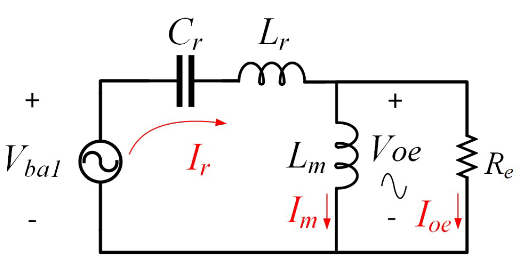
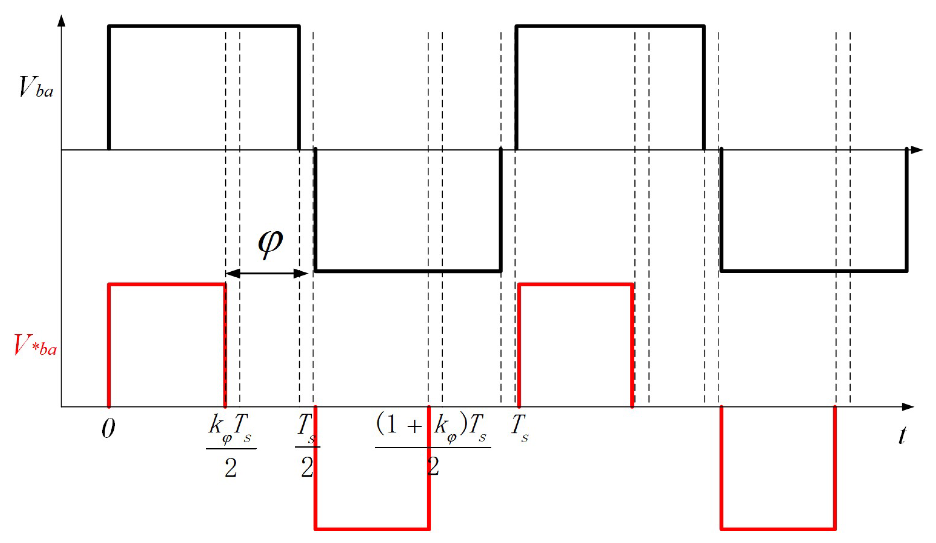
The conventional first harmonic approximation (FHA) is also valid for analyzing the voltage gain function of L L C under VFAPS scheme. Figure 8 shows the FHA model of L L C . The essential distinction between the voltage gain in FM and VFAPS schemes is the different equivalent output resistance R e caused by input functions. Figure 9 shows the waveforms of V b a under two modulation schemes. V b a under a traditional FM scheme could be expressed as a square wave as (58) shows. V b a 1 is the fundamental component of V b a , whose RMS value is 2 2 π V b a . V o e is the reflected AC output, whose RMS value is 2 2 π n V o . According to [30], R e is thus deduced as R e = 8 n 2 π 2 R L . By analyzing the FHA circuit of L L C in the frequency domain, the normalized voltage gain G = n V o / V i n under the FM scheme can be thus expressed as (59) shows:
V b a ( t ) = V i n 2 0 < t T s / 2 V i n 2 T s / 2 < t T s
G = 1 ( 1 + L r L m L r L m ( f r 1 f s ) 2 ) 2 + ( Q e ( f s f r 1 f r 1 f s ) ) 2
where the quality factor Q e = L r / C r R e .
As for L L C modulated by the VFAPS scheme, the square-waved V b a * in the time-domain can be given by
V b a * ( t ) = V i n 2 0 < t k φ T s / 2 0 k φ T s / 2 < t < T s / 2 V i n 2 T s / 2 < t ( 1 + k φ ) T s / 2 0 ( 1 + k φ ) T s / 2 < t < T s
where k φ is defined as the PS angle ratio and can be expressed as k φ = 2 ( π φ ) T s w r 1 .
Thus, the fundamental component of V b a * can be expressed by
V b a 1 * ( t ) = V i n 2 π a 1 c o s 2 π f s t + V i n 2 π b 1 s i n 2 π f s t = V i n 2 π a 1 2 + b 1 2 s i n ( 2 π f s t φ v )
where a 1 = s i n k φ π s i n ( 1 + k φ ) π , b 1 = c o s k φ π + c o s ( 1 + k φ ) π + 2 , φ v = a r c t a n ( b 1 / a 1 ) .
On the output side, the fundamental component of V o e ( t ) can be approximated as
V o e 1 * ( t ) = n V o π a 1 2 + b 1 2 s i n ( 2 π f s t φ v φ v 1 )
where φ v 1 is the phase angle between V b a * and V o e * .
The RMS value of V o e * ( t ) can be given by
V o e 1 R M S * = 2 n V o 2 π a 1 2 + b 1 2
According to the law of conservation of energy, the RMS value of the equivalent output current I o e * could be given by
P o = V o e 1 R M S * I o e 1 R M S * = V o I o I o e 1 R M S * = 2 π I o n a 1 2 + b 1 2 .
Consequently, the R e * under VFAPS modulation scheme could be deduced as follows:
R e * = V o e 1 R M S * I o e 1 R M S * = n 2 ( a 1 2 + b 1 2 ) 2 π 2 R L .
Replacing R e with R e * in (59), the voltage gain function under VFAPS modulation scheme could be given by
G * = 1 ( 1 + L r L m L r L m ( f r 1 f s ) 2 ) 2 + ( Q e * ( f s f r 1 f r 1 f s ) ) 2
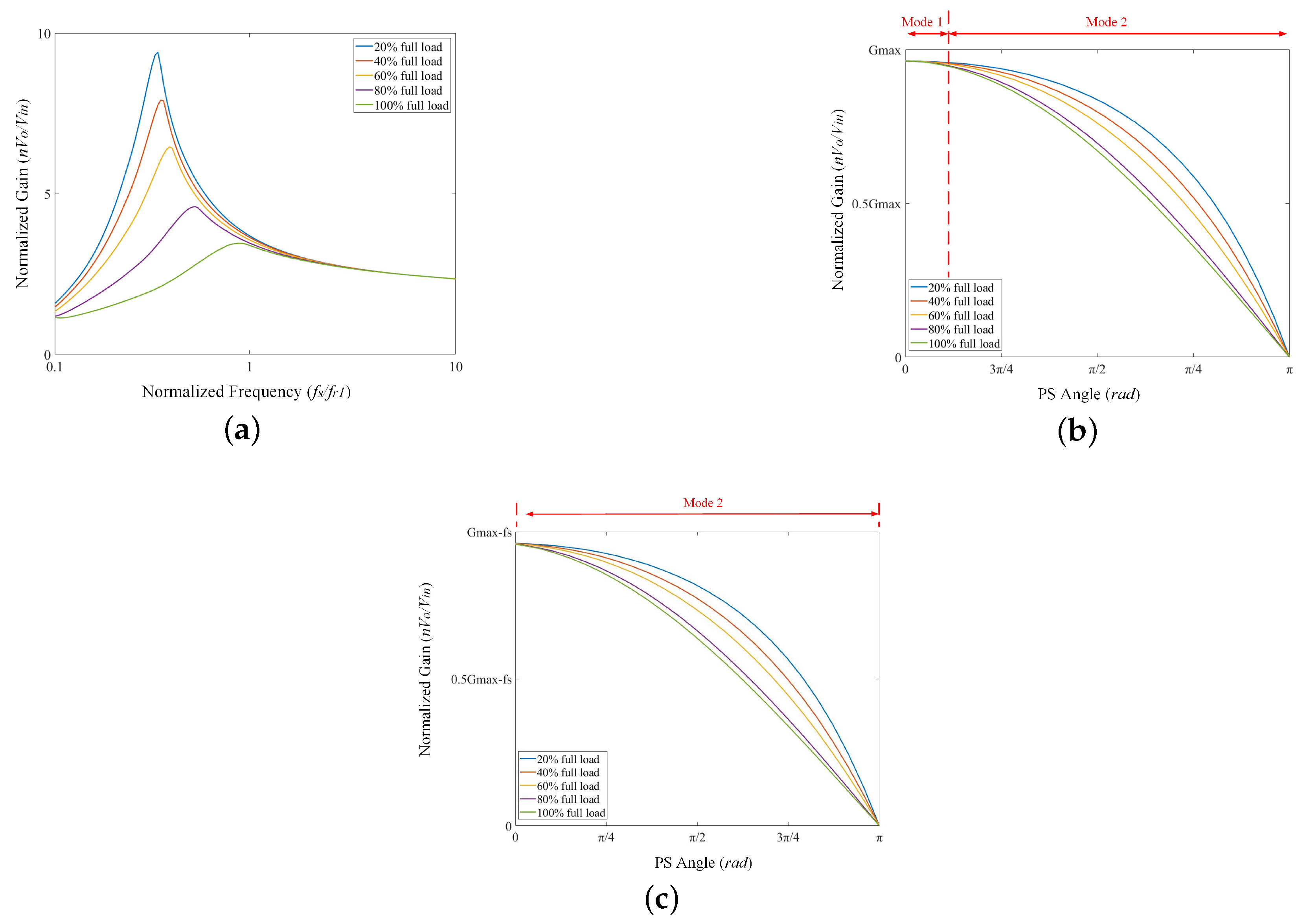
Figure 10 shows the C++Builder6-simulated variation in G under VFAPS scheme with different Q e . Figure 10a shows the relationship between G and normalized f s / f r 1 with no φ modulated. Its gain variation makes no difference from it modulated by the FM scheme. The variation of G shows a non-monotonous tendency when f s changes, making G hard to predict. Moreover, the high step-down ratio is hard to achieve under heavy load conditions. Figure 10b shows the relationship between G and φ under a specified f s ( f r 2 < f s < f r 1 ). The G m a x here indicates the peak gain under the specified f s . The red dotted line divides the zoom into Mode 1 and Mode 2. When φ [0, w r 2 t x ], the converter operates in Mode 1. Since the variation of φ in Mode 1 is fairly limited and is applied to the reactive current, its gain range is very narrow. However, if φ is further increased and ∈( w r 2 t x , w r 2 t x + w r 1 ( T s 2 t x ) ), the converter will conduct in Mode 2. Its gain range is much wider and decreases monotonously with the increment in φ . Figure 10c shows the relationship between G and φ when f s > f r 1 . As long as φ > 0 , the converter could operate in Mode 2. The simulation is consistent with the analysis in Section 2.2. Combined with FM scheme, this VFAPS could effectively broaden the gain range in the buck region. Moreover, this monotonous modulation could further reduce the control complexity.

4. Experimental Verification

To verify the effectiveness of this T-type TL L L C resonant converter with its VFAPS modulation scheme, this section will mainly analyze its performance from several aspects, including reverse recovery loss, conduction loss, and conversion efficiency.

4.1. Prototype

As Figure 11 shows, a 500-W prototype with 650∼950-V input voltage and 48-V/11-A output rating conditions have been established using the components listed in Table 2. The drive signal is controlled by the FPGA EP4CE6F17C8 of Cyclone IV E, which is from ALTERA company in Santa Clara, CA, USA, and its main components are made in South Korea. Considering the PCB layout and the leakage inductance of the transformer, L r is a bit larger than the theoretical results.

4.2. Steady-State Waveforms

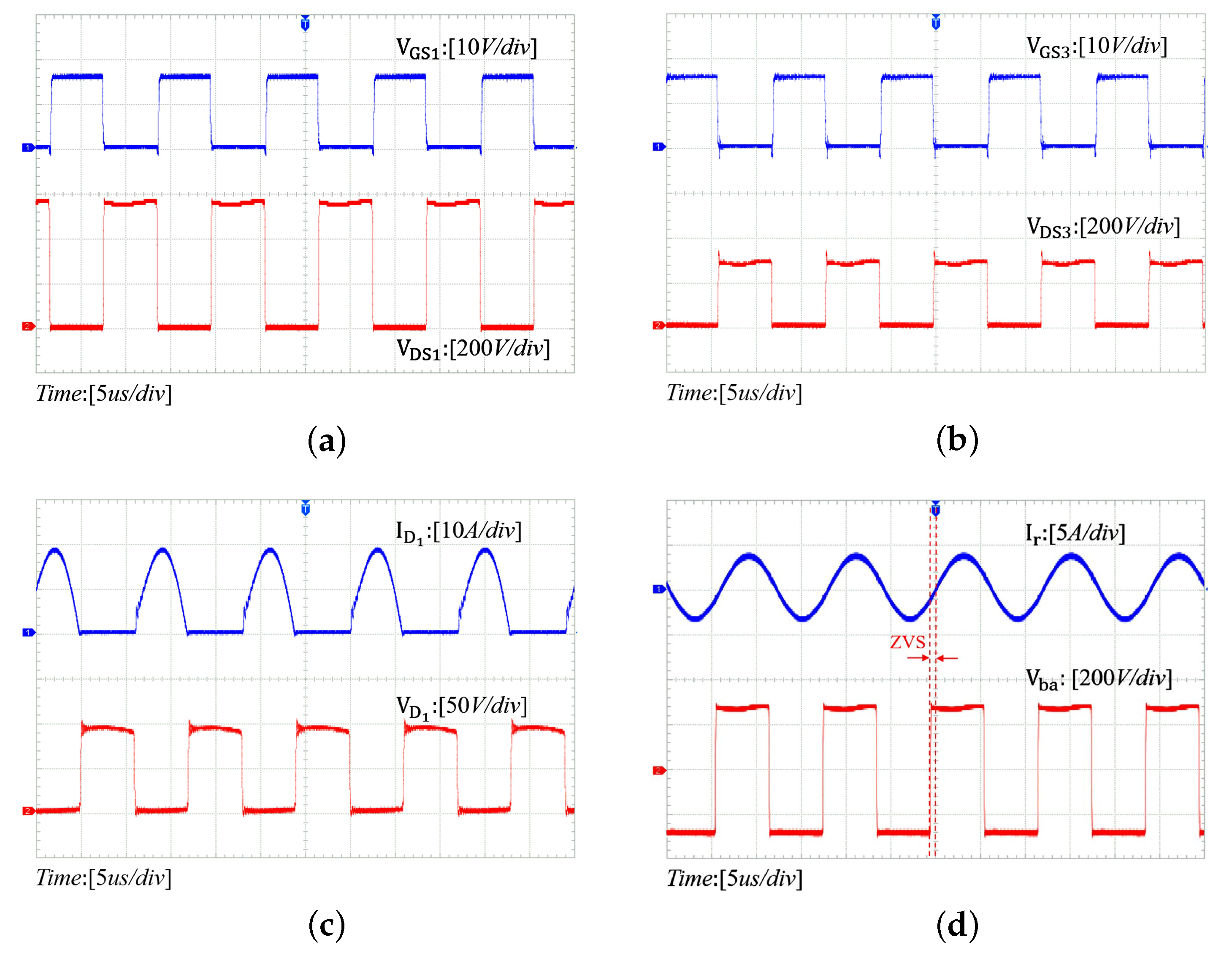
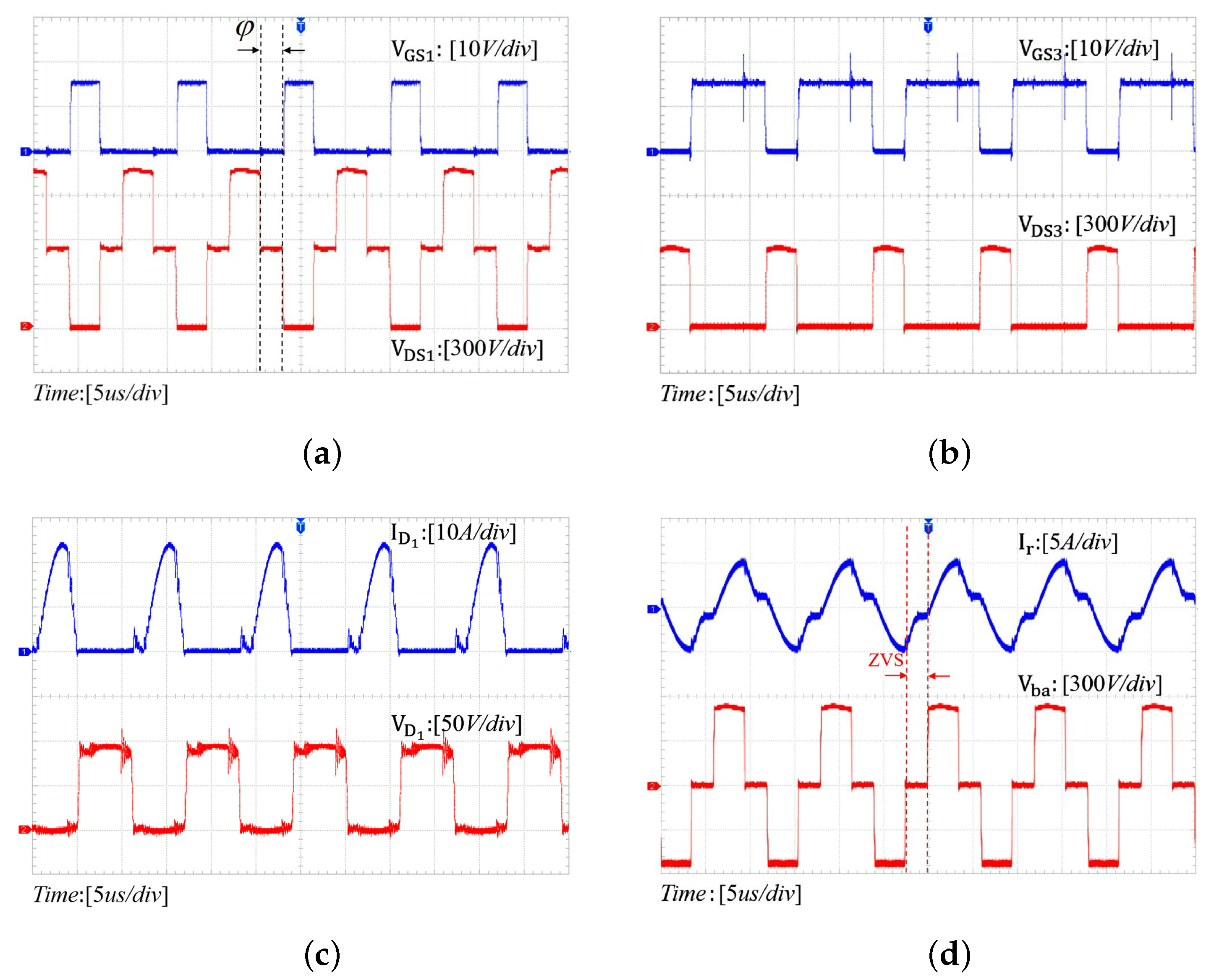
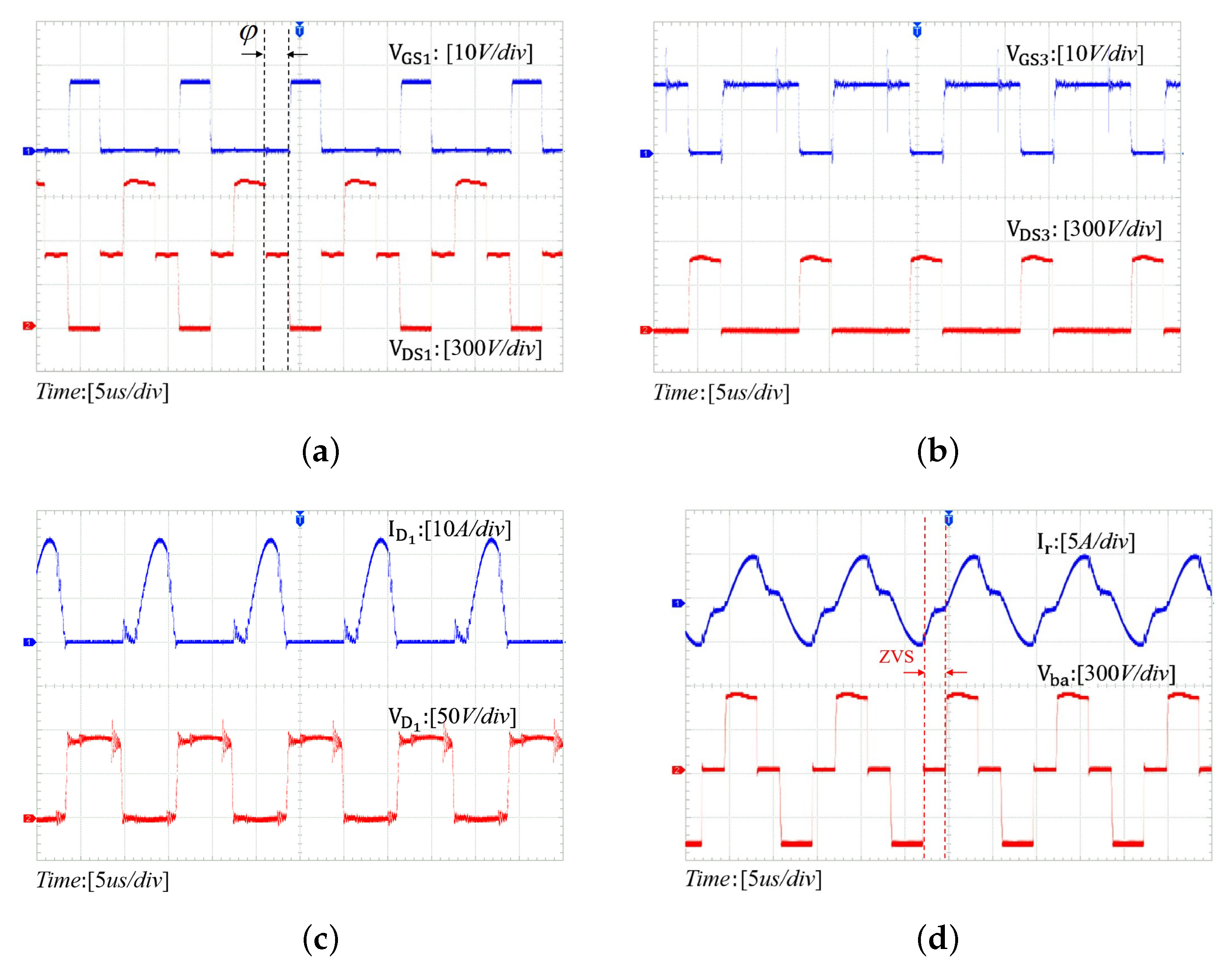
Figure 12 and Figure 13 show the steady-state waveforms of the T-type operating at f r 1 under the full-load condition. Figure 12 shows the waveforms when f s = f r 1 , φ = 0 , and its V i n could reach 650 V. In this situation, Q 1 , Q 2 are driven complementarily, and T-type operates exactly the same as HB L L C . Figure 13 shows the waveforms when f s = f r 1 , φ = 7 π / 10 , its V i n could reach 950 V. Compared with FM, VFAPS is able to satisfy wide input (650∼950 V) at fixed frequency, which could effectively reduce the turn-off loss and control complexity. Figure 14 and Figure 15 show the waveforms with a wide input (650∼950 V) under the full load condition when f s is above and below the f r 1 , respectively. Figure 14 shows the waveforms when f r 2 < f s < f r 1 ( f s = 79.36 kHz), its φ is set as 2 π / 3 to achieve V i n = 950 V. The φ in f r 2 < f s < f r 1 is a bit smaller than that in f s = f r 1 , which is consistent with the gain variation in Section 3.6. Figure 15 show the waveforms when f s > f r 1 ( f s = 90.92 kHz), the φ is set as 3 π / 5 to achieve V i n = 650 V. It is concluded the wide input range could be achieved both below and above the f r 1 . Furthermore, the zoom framed by the red dotted line in the waveforms of I r and V b a shows that ZVS could be ensured under these conditions.
Moreover, the voltage stress on Q 3 , Q 4 is V i n 2 , which is only half of that on Q 1 , Q 2 . That is to say, while selecting devices, a high voltage rating and fast-switching switches, like 1200-V SiC MOSFET, should be selected for Q 1 , Q 2 to reduce the turn-off loss. However, low voltage rating switches, like 650-V SiC or Si MOSFET, are allowed for Q 3 , Q 4 , for the advantages of low voltage stress, fast discharging process, low conduction loss, and very low turn-off loss on the auxiliary leg. Utilizing low voltage rating switches could effectively save cost without affecting the switching rate. Table 3 has listed the reverse recovery loss under the above four conditions, and their values are almost negligible. In other words, ZCS of the secondary rectifier diodes could be ensured as well.

4.3. The Conversion Efficiency

Figure 16 shows the conversion efficiency under different load (20%, 40%, 60%, 80%, 100%) and input (650, 750, 850, 950 V) conditions. It is observed that the conversion efficiency will increase with the rise in load current when φ is comparatively small. However, if φ is large enough to shut off I r ( t ) at its peak value, the turn-off current will be relatively higher, which will accordingly increase the turn-off loss. Moreover, when input increases, φ will be accordingly prolonged to keep the stable output. This will increase the conducting current for switches, thus decreasing the efficiency.
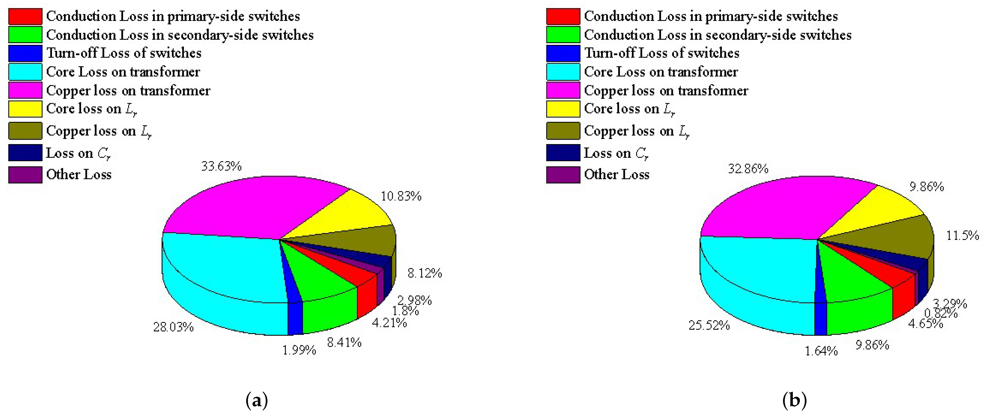
Figure 17 shows the proportion of different losses under varying V i n (650, 950 V) and full conditions. In addition to conduction loss and switching loss, there are also other loss parts. The core loss mainly stems from L r and transformer, which could be estimated from the relation curve of the f s and magnetic flux density provided by the manufacturer. The copper loss is the heat loss caused by current flowing through the windings, which could be estimated by the skin effect. The loss on C r is caused by energy dissipation in the dielectric material, which could be calculated by the dielectric loss. These losses are calculated via the formulas presented in [31]. Compared with the 650-V input, the higher conducting current and prolonged φ in 950-V input will induce higher conduction loss, higher turn-off loss, and higher core loss.

5. Conclusions

In this work, a high step-down SiC-based T-type TL L L C resonant converter has been demonstrated for the spacecraft PPU. The VFAPS modulation scheme is further proposed to achieve wide gain range, high buck, and high efficiency. The mechanism and boundary conditions for achieving soft switching have been analyzed in detail. Moreover, guidance for the proposed VFAPS parameter settings and the optimal L L C design considerations have been elaborated. The ZVS for all the primary switches and low turn-off loss for auxiliary switches among the varying load conditions could be achieved. In addition, only one primary switch suffers from the conduction loss during most of the operation modes, which will effectively improve the overall conversion efficiency.

Author Contributions

Conceptualization, W.M.; Methodology, W.M.; Software, W.M.; Validation, W.M.; Resources, H.L. All authors have read and agreed to the published version of the manuscript.

Funding

Aircraft Swarm Intelligent Sensing and Cooperative Control Key Laboratory of Sichuan Province.

Data Availability Statement

Data available on request due to restrictions.

Conflicts of Interest

The authors declare no conflicts of interest.

References

  1. Wang, L.; Zhang, D.; Duan, J.; Li, J. Design and research of high voltage power conversion system for space solar power station. In Proceedings of the 2018 IEEE International Power Electronics and Application Conference and Exposition (PEAC), Shenzhen, China, 4–7 November 2018; IEEE: Piscataway, NJ, USA, 2018; pp. 1–5. [Google Scholar]
  2. Fang, M.; Zhang, D.; Qi, X. A novel power processing unit (PPU) system architecture based on HFAC bus for electric propulsion spacecraft. IEEE J. Emerg. Sel. Top. Power Electron. 2022, 10, 5381–5391. [Google Scholar] [CrossRef]
  3. Osuga, H.; Kurokawa, F. Power Processing Unit for the next generation satellite. In Proceedings of the 2009 13th European Conference on Power Electronics and Applications, Barcelona, Spain, 8–10 September 2009; IEEE: Piscataway, NJ, USA, 2009; pp. 1–8. [Google Scholar]
  4. Carr, G.A.; Iannello, C.J.; Chen, Y.; Hunter, D.J.; Del Castillo, L.; Bradley, A.T.; Stell, C.; Mojarradi, M.M. Extreme environment capable, modular and scalable power processing unit for solar electric propulsion. In Proceedings of the 2013 IEEE Aerospace Conference, Big Sky, MT, USA, 2–9 March 2013; IEEE: Piscataway, NJ, USA, 2013; pp. 1–9. [Google Scholar]
  5. Huang, X.; Lan, J.; Chen, N.; Fang, T.; Ruan, X.; He, X. A novel two-stage DC/DC converter applied to power processing unit for astronautical ion propulsion system. In Proceedings of the 2019 IEEE International Conference on Industrial Technology (ICIT), Melbourne, Australia, 13–15 February 2019; IEEE: Piscataway, NJ, USA, 2019; pp. 343–348. [Google Scholar]
  6. Hassanzadeh, N.; Yazdani, F.; Haghbin, S.; Thiringer, T. Design of a 50 kw phase-shifted full-bridge converter used for fast charging applications. In Proceedings of the 2017 IEEE Vehicle Power and Propulsion Conference (VPPC), Belfort, France, 11–14 December 2017; IEEE: Piscataway, NJ, USA, 2017; pp. 1–5. [Google Scholar]
  7. Bonten, R.W.T.; Schellekens, J.M.; Vermulst, B.J.D.; Clermonts, F.M.; Huisman, H. Improved Dynamic Behavior for the Series-Resonant Converter Using Bidirectional Charge Control. IEEE Trans. Power Electron. 2022, 37, 11607–11619. [Google Scholar] [CrossRef]
  8. Kim, J.W.; Barbosa, P. PWM-controlled series resonant converter for universal electric vehicle charger. IEEE Trans. Power Electron. 2021, 36, 13578–13588. [Google Scholar] [CrossRef]
  9. Saha, T.; Wang, H.; Riar, B.; Zane, R. Analysis and Design of a Parallel Resonant Converter for Constant Current Input to Constant Voltage Output DC-DC Converter Over Wide Load Range. In Proceedings of the 2018 International Power Electronics Conference (IPEC-Niigata 2018-ECCE Asia), Niigata, Japan, 20–24 May 2018. [Google Scholar]
  10. Vakacharla, V.R.; Rathore, A.K. Isolated Soft Switching Current Fed LCC-T Resonant DC–DC Converter for PV/Fuel Cell Applications. IEEE Trans. Ind. Electron. 2019, 66, 6947–6958. [Google Scholar] [CrossRef]
  11. Vakacharla, V.R.; Rathore, A.; Singh, R.; Mishra, S. Fixed-Frequency Current-Fed LCL Series Resonant Soft-Switching Converter with Capacitive Doubler. IEEE Trans. Ind. Appl. 2021, 57, 6611–6621. [Google Scholar] [CrossRef]
  12. Wang, H.; Li, Z. A PWM LLC Type Resonant Converter Adapted to Wide Output Range in PEV Charging Applications. IEEE Trans. Power Electron. 2017, 33, 3791–3801. [Google Scholar] [CrossRef]
  13. Colak, K.; Asa, E.; Czarkowski, D. A comparison analysis of CLL and LLC resonant converter for multi-phase applications. In Proceedings of the 2015 IEEE Transportation Electrification Conference and Expo (ITEC), Dearborn, MI, USA, 14–17 June 2015; pp. 1–6. [Google Scholar] [CrossRef]
  14. Patil, U.; Nagendrappa, H. Analysis and Design of a Three Phase Interleaved CLL Resonant Converter with Fixed Frequency Modified PWM Control. In Proceedings of the 2021 IEEE 6th International Conference on Computing, Communication and Automation (ICCCA), Arad, Romania, 17–19 December 2021; pp. 144–149. [Google Scholar] [CrossRef]
  15. Chen, Y.; Wang, H.; Hu, Z.; Liu, Y.; Liu, X.; Afsharian, J.; Yang, Z. LCLC Converter with Optimal Capacitor Utilization for Hold Up Mode Operation. IEEE Trans. Power Electron. 2018, 34, 2385–2396. [Google Scholar] [CrossRef]
  16. Yin, S.; Xin, X.; Wang, R.; Dong, M.; Lin, J.; Gu, Y.; Li, H. A 1-MHz GaN-Based LCLC Resonant Step-Up Converter with Air-Core Transformer for Satellite Electric Propulsion Application. IEEE Trans. Ind. Electron. 2022, 69, 11035–11045. [Google Scholar] [CrossRef]
  17. Wen, H.; Jiao, D.; Lai, J.S.; Strydom, J.; Lu, B. A MHz LCLCL Resonant Converter Based Single-Stage Soft-Switching Isolated Inverter with Variable Frequency Modulation. In Proceedings of the 2022 IEEE Applied Power Electronics Conference and Exposition (APEC), Houston, TX, USA, 20–24 March 2022; pp. 848–854. [Google Scholar] [CrossRef]
  18. Yang, Y.; Liu, X.; Zhang, H.; Shi, Y. A Dual Coupling LCC-LCC Topology Based WPT System for Wireless Slip Ring. In Proceedings of the 2023 IEEE 2nd International Conference on Electrical Engineering, Big Data and Algorithms (EEBDA), Changchun, China, 24–26 February 2023; pp. 1333–1336. [Google Scholar] [CrossRef]
  19. Rodríguez, G.N.; Martínez, M.A.; Zajc, A.; Zajc, F.; Cabanuz, J.T.; Zajc, F.; Hortal, R.R.; Cervera, P.A. Isolated DC/DC Converter for RF generator of a Power Propulsion Unit: Topology Comparison Based on GaN Semiconductors. In Proceedings of the 2023 13th European Space Power Conference (ESPC), Elche, Spain, 2–6 October 2023; IEEE: Piscataway, NJ, USA, 2023; pp. 1–6. [Google Scholar]
  20. Jie, X.; Qing, K.; Xuan, Z.; Feng, L. Application prospect of SiC power semiconductor devices in spacecraft power systems. In Proceedings of the 2017 13th IEEE International Conference on Electronic Measurement & Instruments (ICEMI), Yangzhou, China, 20–22 October 2017; IEEE: Piscataway, NJ, USA, 2017; pp. 185–190. [Google Scholar]
  21. Piñero, L.R.; Scheidegger, R.J.; Aulsio, M.V.; Birchenough, A.G. High input voltage discharge supply for high power hall thrusters using silicon carbide devices. In Proceedings of the International Electric Propulsion Conference (IEPC2013), Washington, DC, USA, 6–10 October 2013. number NASA/TM-2014-216607. [Google Scholar]
  22. Fu, D.; Lee, F.C.; Qiu, Y.; Wang, F. A novel high-power-density three-level LCC resonant converter with constant-power-factor-control for charging applications. IEEE Trans. Power Electron. 2008, 23, 2411–2420. [Google Scholar] [CrossRef]
  23. Choudhury, A.; Pillay, P. Space Vector Based Capacitor Voltage Balancing for a Three-Level NPC Traction Inverter Drive. IEEE J. Emerg. Sel. Top. Power Electron. 2020, 8, 1276–1286. [Google Scholar] [CrossRef]
  24. Narimani, M.; Wu, B.; Cheng, G.; Zargari, N. A new nested neutral point clamped (NNPC) converter for medium-voltage (MV) power conversion. In Proceedings of the 2014 IEEE Applied Power Electronics Conference and Exposition—APEC 2014, Fort Worth, TX, USA, 16–20 March 2014; pp. 2372–2377. [Google Scholar] [CrossRef]
  25. Khoshkbar Sadigh, A.; Abarzadeh, M.; Corzine, K.A.; Dargahi, V. A New Breed of Optimized Symmetrical and Asymmetrical Cascaded Multilevel Power Converters. IEEE J. Emerg. Sel. Top. Power Electron. 2015, 3, 1160–1170. [Google Scholar] [CrossRef]
  26. Belkhode, S.; Rao, P.; Shukla, A.; Doolla, S. Comparative Evaluation of Silicon and Silicon-Carbide Device-Based MMC and NPC Converter for Medium-Voltage Applications. IEEE J. Emerg. Sel. Top. Power Electron. 2022, 10, 856–867. [Google Scholar] [CrossRef]
  27. Sun, Z.; Peng, F.; Magne, P.; Emadi, A. A Phase Shifted Full Bridge Converter with ZCS Synchronous Rectifier for Auxiliary Power Units. In Proceedings of the IECON 2014—40th Annual Conference of the IEEE Industrial Electronics Society, Dallas, TX, USA, 29 October–1 November 2014; IEEE: Piscataway, NJ, USA, 2014; pp. 2945–2951. [Google Scholar]
  28. Yu, M.; Sha, D.; Guo, Z.; Liao, X. Hybrid PS Full Bridge and LLC Half Bridge DC/DC Converter for Low-Voltage and High-Current Output Applications. In Proceedings of the 2014 IEEE Applied Power Electronics Conference and Exposition—APEC 2014, Fort Worth, TX, USA, 16–20 March 2014; IEEE: Piscataway, NJ, USA, 2014; pp. 1088–1094. [Google Scholar]
  29. Kalayci, K.; Demirel, O.; Arifoglu, U.; Hizarci, H. Analysis of Three-Level T-Type LLC Resonant Isolated Bidirectional DC–DC Converter Under Three-Degrees-of-Freedom Modulation. IEEE Access 2023, 11, 60605–60625. [Google Scholar] [CrossRef]
  30. Huang, H. Designing an LLC resonant half-bridge power converter. In Proceedings of the 2010 Texas Instruments Power Supply Design Seminar, SEM1900, Topic; Texas Instruments Incorporated Dallas: Dallas, TX, USA, 2010; Volume 3, pp. 2010–2011. Available online: https://www.ti.com.cn/cn/lit/pdf/ssztch0 (accessed on 1 May 2024).
  31. Erickson, R.W.; Maksimovic, D. Fundamentals of Power Electronics; Springer Science & Business Media: Berlin/Heidelberg, Germany, 2007. [Google Scholar]
Figure 1. Two-stage spacecraft solar PPU.
Aerospace 11 00396 g001
Figure 2. T-type L L C resonant converter topology.
Aerospace 11 00396 g002
Figure 3. Steady-state switching waveforms in different mode: (a) HB Mode, (b) Mode 1, (c) Mode 2.
Aerospace 11 00396 g003
Figure 4. Equivalent circuits of each stage: (a) [ t 0 , t 1 ], (b) [ t 1 , t 2 ], (c) [ t 2 , t 4 ], (d) [ t 4 , t 5 ], (e) [ t 5 , t 6 ], (f) [ t 6 , t 7 ], (g) [ t 7 , t 9 ], (h) [ t 9 , t 10 ].
Aerospace 11 00396 g004
Figure 5. Steady-state waveforms of Mode 2 without dead times. (Purple: I r , black: I m , blue: V C r , green: I D ).
Aerospace 11 00396 g005
Figure 6. Steady-state waveforms of Mode 2 with boundary conditions: (a) steady-state waveforms under limiting soft-switching conditions, (b) steady-state waveforms under V i n m i n when f r 2 < f s < f r 1 . (Purple: I r , black: I m , blue: V C r , green: I D .)
Aerospace 11 00396 g006
Figure 7. VFAPS design flowchart.
Aerospace 11 00396 g007
Figure 8. First harmonic approximation of L L C .
Aerospace 11 00396 g008
Figure 9. The schematic of V b a under FM and VFAPS scheme.
Aerospace 11 00396 g009
Figure 10. Simulation of normalized voltage gain: (a) normalized voltage gain under FM scheme when L n = 5, (b) normalized voltage gain under PS scheme with a specified f s ( f r 2 < f s < f r 1 ), (c) normalized voltage gain under PS scheme with a specified f s ( f s > f r 1 ).
Aerospace 11 00396 g010
Figure 11. The prototype of T-type L L C resonant converter: (a) driving PCB, (b) primary and secondary side.
Aerospace 11 00396 g011
Figure 12. Steady-state switching waveforms at f r 1 with φ = 0 : (a) V G S 1 and V D S 1 , (b) V G S 3 and V D S 3 , (c) I D 1 and V D 1 , (d) I r and V b a .
Aerospace 11 00396 g012
Figure 13. Steady-state switching waveforms at f r 1 with φ = 7 π / 10 : (a) V G S 1 and V D S 1 , (b) V G S 3 and V D S 3 , (c) I D 1 and V D 1 , (d) I r and V b a .
Aerospace 11 00396 g013
Figure 14. Steady-state switching waveforms operating at 79.36 kHz with φ = 2 π / 3 : (a) V G S 1 and V D S 1 , (b) V G S 3 and V D S 3 , (c) I D 1 and V D 1 , (d) I r and V b a .
Aerospace 11 00396 g014
Figure 15. Steady-state waveforms operating at 90.92 kHz with φ = 3 π / 5 : (a) V G S 1 and V D S 1 , (b) V G S 3 and V D S 3 , (c) I D 1 and V D 1 , (d) I r and V b a .
Aerospace 11 00396 g015
Figure 16. The conversion efficiency.
Aerospace 11 00396 g016
Figure 17. Theoretical efficiency of measured results under different input and full load conditions: (a) 650 V, (b) 950 V.
Aerospace 11 00396 g017
Table 1. Comparisons among multi-levels.
TopologyAdvantageDisadvantage
NPCSimple structure;
Low voltage stress;
Good dynamic response;
Low EMI.
Extra conduction loss
for freewheeling diodes;
Uneven distributed losses.
ANPCSimple structure;
Low voltage stress;
Good dynamic response;
Low EMI;
Improved Efficiency
comparing to NPC.
High cost;
More complex modulation
scheme comparing to NPC.
NNPCLess components
comparing to NPC.
Can not be applied
to higher levels.
CHBModular structure;
High reliability;
fault-tolerant features.
Isolated DC links.
MMCModular structure;
High reliabilty;
More balanced loss distribution
and less harmonics
comparing to NPC.
More bulky capacitances
comparing to NPC;
Precharging process.
FBLow current stress
comparing to NPC;
Low conduction loss
comparing to NPC.
High cost;
High voltage stress;
High insulation and high
withstand voltage for transformer;
High rated voltage
for passive components;
Worse EMI comparing to NPC.
T-typeLow voltage stress for
switches on auxiliary leg
comparing to NPC;
Low conduction loss
comparing to NPC;
Low turn-off current for
switches on auxiliary leg;
No floating capacitances;
Low EMI.
High voltage stress for main switches.
Table 2. Components list.
ParametersValue/Type
Input voltage ( V i n )650∼950 V
Resonant inductor ( L r )110 μ H
Resonant capacitor ( C r )0.025 cuF
Turns ratio of transformer (n)6
magnetizing inductor ( L m )450.4 μ H
Filter capacitor ( C o )470 μ F
Resonant frequency of L r , C r ( f r 1 ) 83 kHz
Resonant frequency of L r , L m , C r ( f r 2 ) 41 kHz
MOSFETs ( Q 1 , Q 2 )C2M0080120D
MOSFETs ( Q 3 , Q 4 )SCT3060AL
Rectifiers ( D 1 , D 2 )MUR6060P
Table 3. Reverse recovery loss under different conditions.
Conditions f s = 83 kHz
φ = 0
f s = 83 kHz
φ = 7 π 10
f s = 79 kHz
φ = 2 π 3
f s = 91 kHz
φ = 3 π 5
Reverse Recovery
Loss (W)
0.070.090.090.07
Disclaimer/Publisher’s Note: The statements, opinions and data contained in all publications are solely those of the individual author(s) and contributor(s) and not of MDPI and/or the editor(s). MDPI and/or the editor(s) disclaim responsibility for any injury to people or property resulting from any ideas, methods, instructions or products referred to in the content.