
Bluetooth Communication Leveraging Ultra-Low Power Radio Design


Abstract
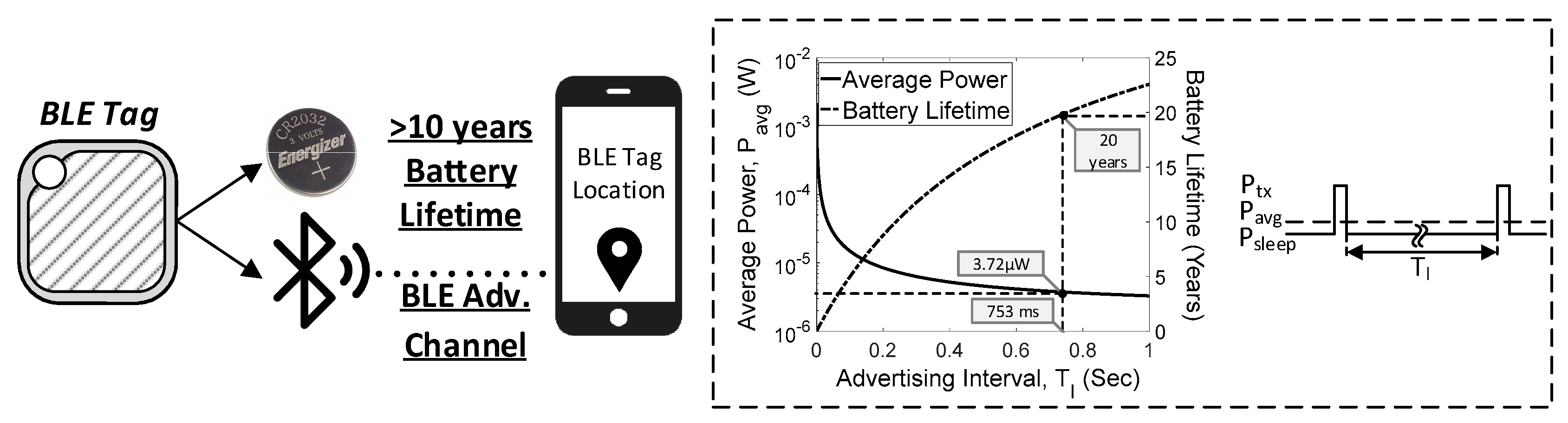
1. Introduction
2. Back-Channel Communication for Energy-Efficient Operation
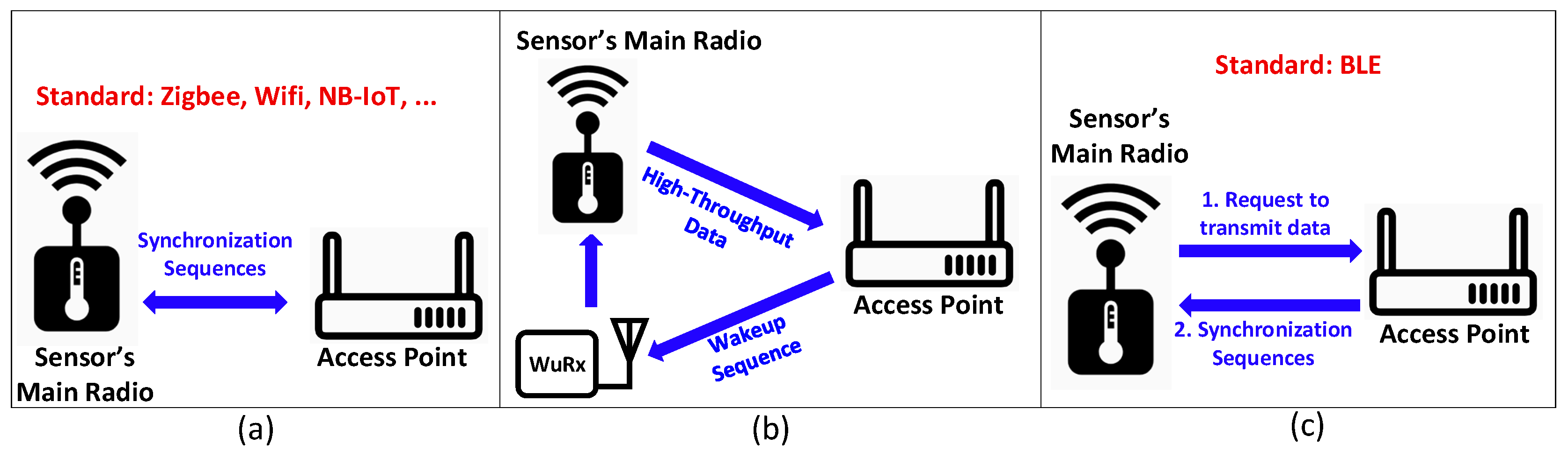
2.1. Synchronization Scehmes
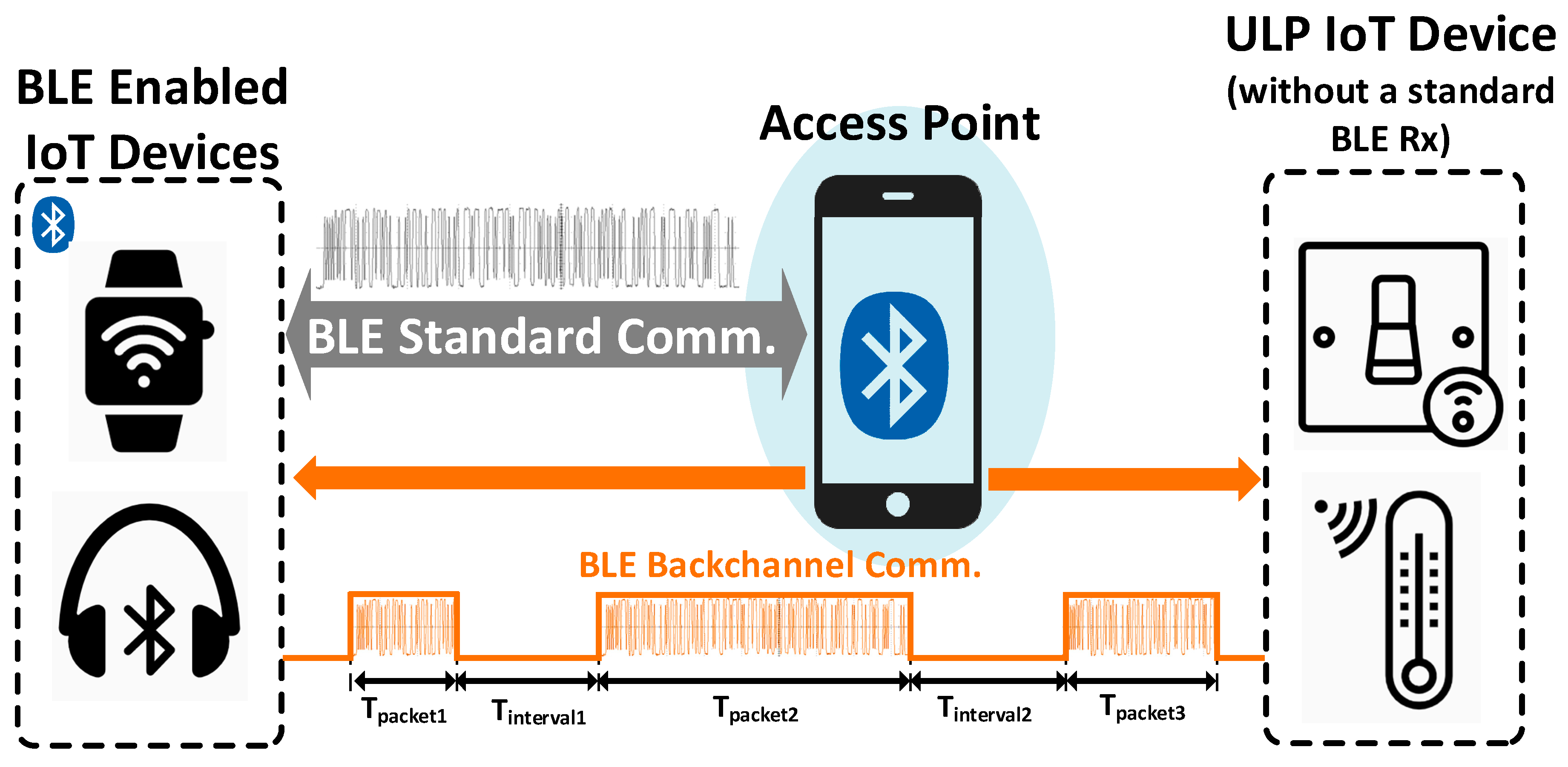
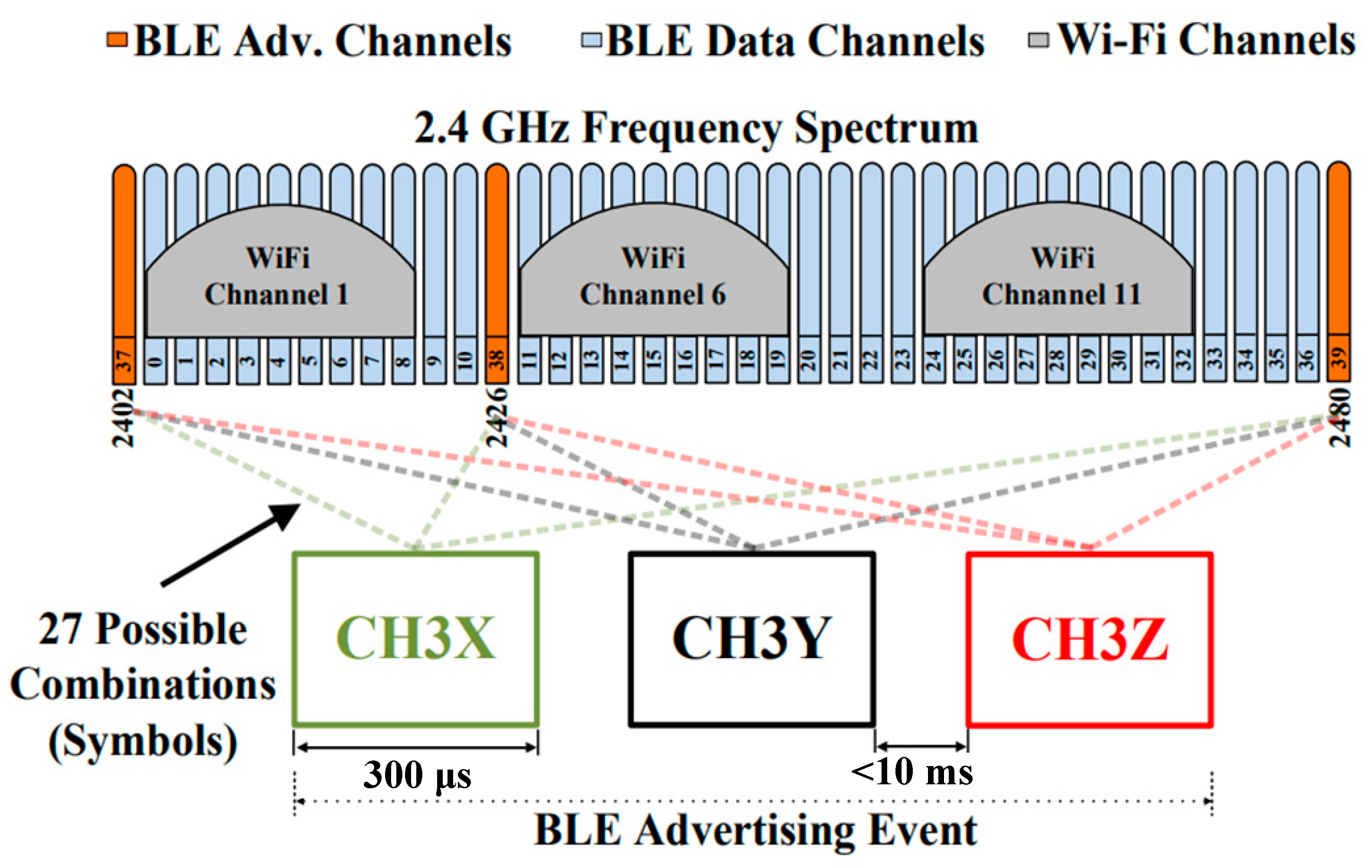
2.2. Back-Channel Communication Concept
2.3. ULP Back-Channel BLE RX Prototype
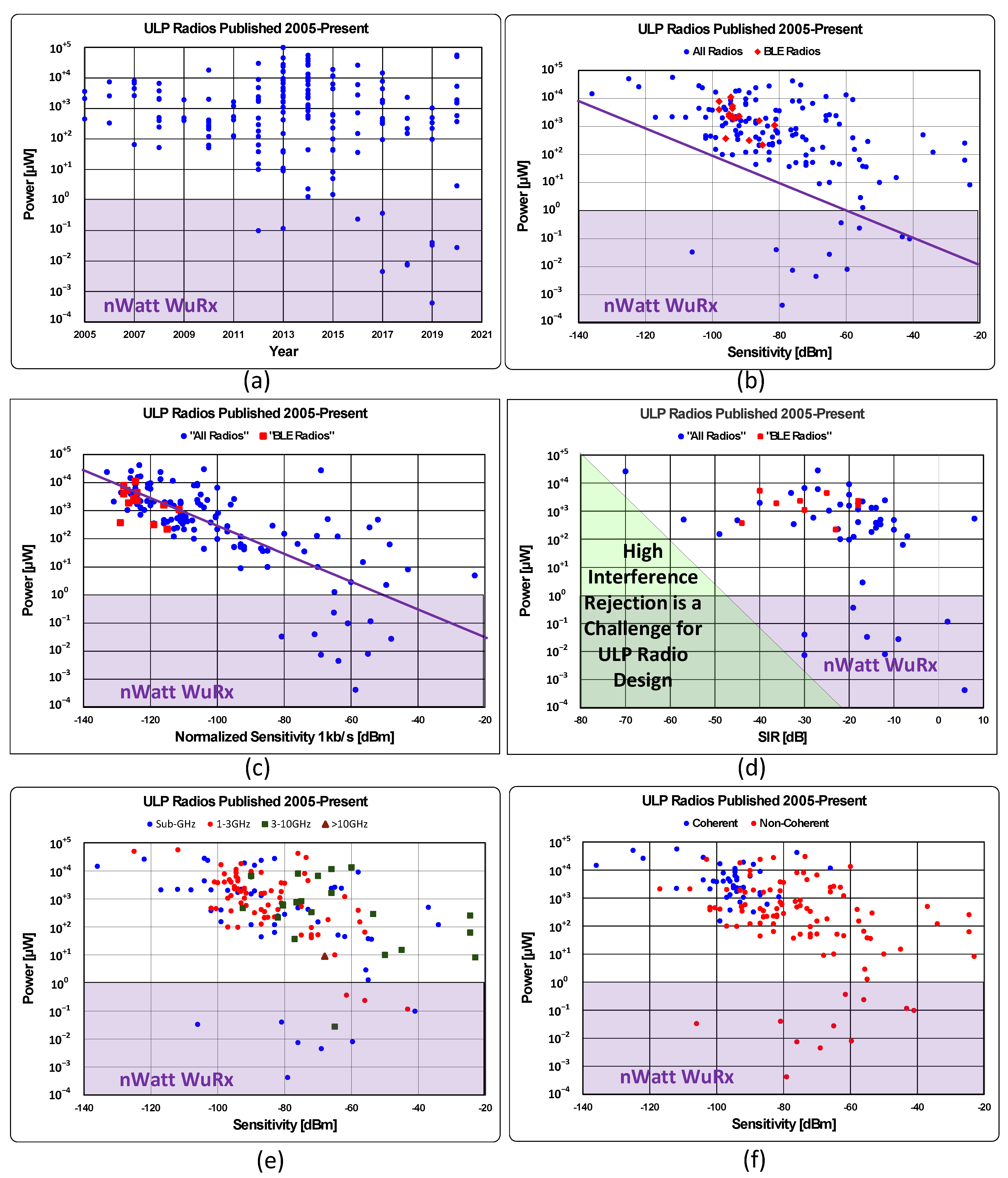
3. BLE Radio Design Trends and Considerations
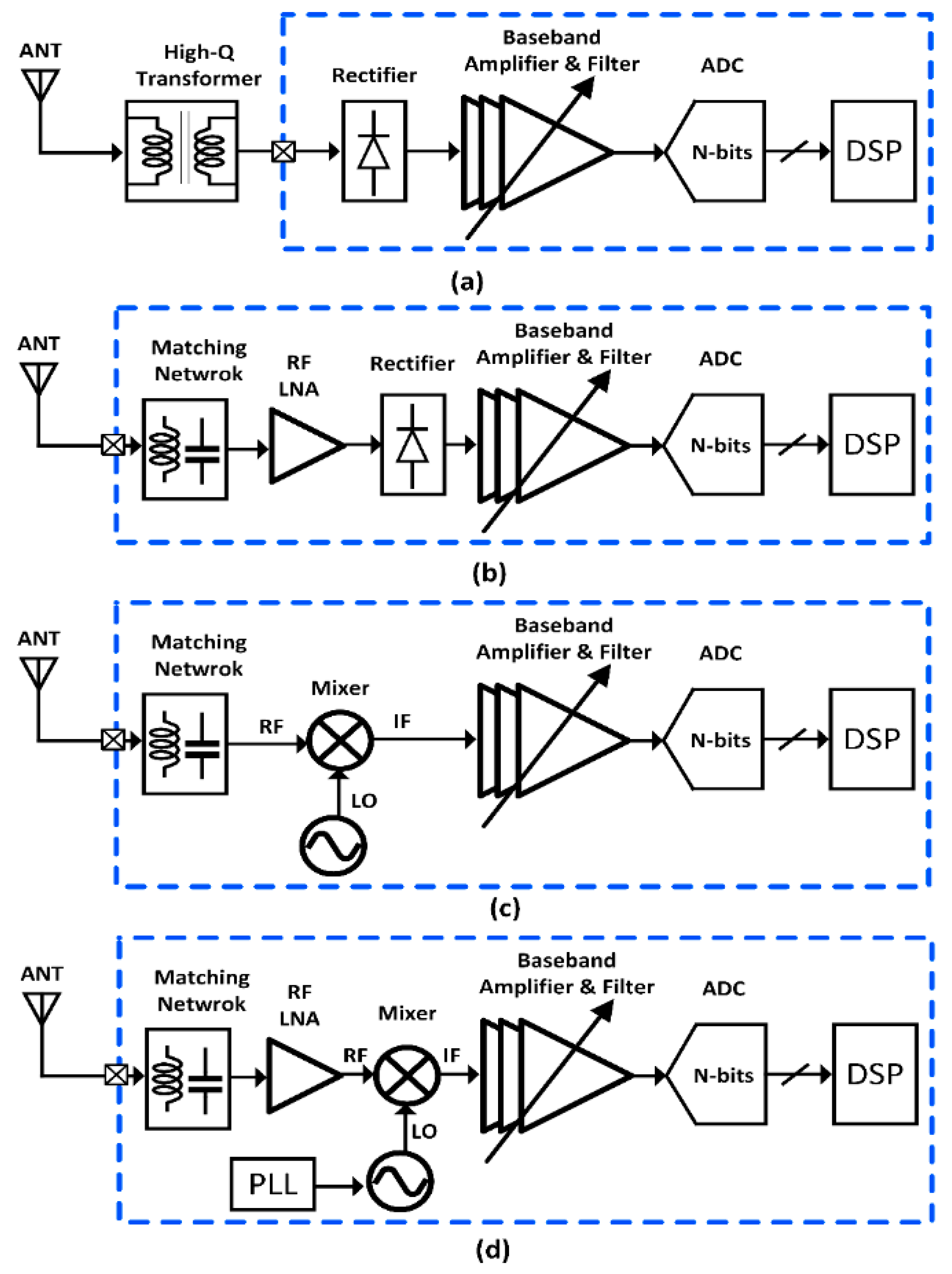
3.1. Receiver Design Trends
3.2. Transmitter Design Trends
3.2.1. Direct GFSK Modulation for Open-Loop LCVCO
3.2.2. Digitization of BLE Transmitters
3.2.3. Reduction of On-Chip/Off-Chip Components
3.2.4. Transmitter-Focused Design Requirement for System Efficiency
4. Conclusions and Future Work
Funding
Informed Consent Statement
Data Availability Statement
Conflicts of Interest
References
- Jeon, K.; She, J.; Soonsawad, P.; Ng, P. BLE Beacons for Internet of Things Applications: Survey, Challenges, and Opportunities. IEEE Internet Things J. 2018, 5, 811–828. [Google Scholar] [CrossRef]
- Bechthum, E.; Dijkhuis, J.; Ding, M.; He, Y.; Van Den Heuvel, J.; Mateman, P.; Van Schaik, G.; Shibata, K.; Song, M.; Tiurin, E.; et al. 30.6 A Low-Power BLE Transceiver with Support for Phase-Based Ranging, Featuring 5 µs PLL Locking Time and 5.3 ms Ranging Time, Enabled by Staircase-Chirp PLL with Sticky-Lock Channel-Switching. In Proceedings of the IEEE International Solid-State Circuits Conference—(ISSCC), San Francisco, CA, USA, 2–6 February 2020; pp. 470–472. [Google Scholar]
- Moosavifar, M.; Wentzloff, D. Analysis of Design Trade-Offs in Ultra Low Power FSK Receivers for Phase-Based Ranging. In Proceedings of the IEEE Topical Conference on Wireless Sensors and Sensor Networks (WiSNeT), San Diego, CA, USA, 23 January 2021. [Google Scholar]
- Zhang, H.; Wentzloff, D.; Kim, H. Software-Defined, WiFi and BLE Compliant Back-Channel for Ultra-Low Power Wireless Communication. In Proceedings of the IEEE Global Communications Conference (GLOBECOM), Washington, DC, USA, 4–8 December 2016; pp. 1–6. [Google Scholar]
- Abdelatty, O.; Bishop, H.; Shi, Y.; Chen, X.; Alghaihab, A.; Calhoun, B.; Wentzloff, D. A Low Power Bluetooth Low-Energy Transmitter with a 10.5 nJ Startup-Energy Crystal Oscillator. In Proceedings of the IEEE 45th European Solid State Circuits Conference (ESSCIRC), Cracow, Poland, 23–26 September 2019; pp. 377–380. [Google Scholar]
- Yang, S.; Yin, J.; Yi, H.; Yu, W.; Mak, P.; Martins, R. A 0.2-V Energy-Harvesting BLE Transmitter With a Micropower Manager Achieving 25% System Efficiency at 0-dBm Output and 5.2-nW Sleep Power in 28-nm CMOS. IEEE J. Solid-State Circuits 2019, 54, 1351–1362. [Google Scholar] [CrossRef]
- Ruiz, L.; Ridder, M.; Fan, D.; Gong, J.; Li, B.; Mills, A.; Cobarrubias, E.; Strohmaier, J.; Jur, J.; Lach, J. Self-Powered Cardiac Monitoring: Maintaining Vigilance with Multi-Modal Harvesting and E-Textiles. IEEE Sens. J. 2021, 21, 2263–2276. [Google Scholar] [CrossRef]
- Li, S.; Breiholz, J.; Kamineni, S.; Im, J.; Wentzloff, D.; Calhoun, B. An 85 nW IoT Node-Controlling SoC for MELs Power-Mode Management and Phantom Energy Reduction. In Proceedings of the IEEE International Symposium on Circuits and Systems (ISCAS), Seville, Spain, 6–9 September 2020; pp. 1–5. [Google Scholar]
- Chen, G.; Ghaed, H.; Haque, R.; Wieckowski, M.; Kim, Y.; Kim, G.; Fick, D.; Kim, D.; Seok, M.; Wise, K.; et al. A cubic-millimeter energy-autonomous wireless intraocular pressure monitor. In Proceedings of the IEEE International Solid-State Circuits Conference (ISSCC), San Francisco, CA, USA, 20–24 February 2011; pp. 310–312. [Google Scholar]
- Sano, T.; Mizokami, M.; Matsui, H.; Ueda, K.; Shibata, K.; Toyota, K.; Saitou, T.; Sato, H.; Yahagi, K.; Hayashi, Y. 13.4 A 6.3 mW BLE transceiver embedded RX image-rejection filter and TX harmonic-suppression filter reusing on-chip matching network. In Proceedings of the IEEE International Solid-State Circuits Conference (ISSCC), San Francisco, CA, USA, 22–26 February 2015; pp. 1–3. [Google Scholar]
- Hanes, D.; Salgueiro, G.; Grossetete, P.; Barton, R.; Henry, J. IoT Fundamentals: Networking Technologies, Protocols, and Use Cases for the Internet of Things; Cisco Press: Indianapolis, IN, USA, 2017; ISBN 9780134307091. [Google Scholar]
- Wang, P.; Mercier, P. An Interference-Resilient BLE-Compatible Wake-Up Receiver Employing Single-Die Multi-Channel FBAR-Based Filtering and a 4-D Wake-Up Signature. IEEE J. Solid-State Circuits 2021, 56, 416–426. [Google Scholar] [CrossRef]
- Wentzloff, D. Low Power Radio Survey. Available online: www.eecs.umich.edu/wics/low_power_radio_survey.html (accessed on 30 March 2021).
- Kim, H.; Wentzloff, D. Back-Channel Wireless Communication Embedded in WiFi-Compliant OFDM Packets. IEEE J. Sel. Areas Commun. 2016, 34, 3181–3194. [Google Scholar] [CrossRef]
- Im, J.; Kim, H.; Wentzloff, D. A 335 µW −72 dBm receiver for FSK back-channel embedded in 5.8 GHz Wi-Fi OFDM packets. In Proceedings of the IEEE Radio Frequency Integrated Circuits Symposium (RFIC), Honolulu, HI, USA, 4–6 June 2017; pp. 176–179. [Google Scholar]
- Alghaihab, A.; Shi, Y.; Breiholz, J.; Kim, H.; Calhoun, B.; Wentzloff, D. Enhanced Interference Rejection Bluetooth Low-Energy Back-Channel Receiver With LO Frequency Hopping. IEEE J. Solid-State Circuits 2019, 54, 2019–2027. [Google Scholar] [CrossRef]
- Brown, J.; Huang, K.; Ansari, E.; Rogel, R.; Lee, Y.; Wentzloff, D. An ultra-low-power 9.8 GHz crystal-less UWB transceiver with digital baseband integrated in 0.18 μm BiCMOS. In Proceedings of the IEEE International Solid-State Circuits Conference (ISSCC), San Francisco, CA, USA, 17–21 February 2013; pp. 442–443. [Google Scholar]
- Abdelhamid, M.; Paidimarri, A.; Chandrakasan, A. A −80 dBm BLE-compliant, FSK wake-up receiver with system and within-bit dutycycling for scalable power and latency. In Proceedings of the IEEE Custom Integrated Circuits Conference (CICC), San Diego, CA, USA, 8–11 April 2018; pp. 1–4. [Google Scholar]
- Tang, S.; Yomo, H.; Takeuchi, Y. Optimization of Frame Length Modulation-Based Wake-Up Control for Green WLANs. IEEE Trans. Veh. Technol. 2015, 64, 768–780. [Google Scholar] [CrossRef]
- Roberts, N.; Craig, K.; Shrivastava, A.; Wooters, S.; Shakhsheer, Y.; Calhoun, B.; Wentzloff, D. 26.8 A 236 nW −56.5 dBm-sensitivity Bluetooth low-energy wakeup receiver with energy harvesting in 65 nm CMOS. In Proceedings of the IEEE International Solid-State Circuits Conference (ISSCC), San Francisco, CA, USA, 31 January–4 February 2016; pp. 450–451. [Google Scholar]
- Roberts, N.; Wentzloff, D. A 98 nW wake-up radio for wireless body area networks. In Proceedings of the IEEE Radio Frequency Integrated Circuits Symposium, Montreal, QC, Canada, 17–19 June 2012; pp. 373–376. [Google Scholar]
- Wentzloff, D.; Alghaihab, A.; Im, J. Ultra-Low Power Receivers for IoT Applications: A Review. In Proceedings of the IEEE Custom Integrated Circuits Conference (CICC), Boston, MA, USA, 22–25 March 2020; pp. 1–8. [Google Scholar]
- Moody, J.; Dissanayake, A.; Bishop, H.; Lu, R.; Liu, N.; Duvvuri, D.; Gao, A.; Truesdell, D.; Barker, N.; Gong, S.; et al. A −106 dBm 33 nW Bit-Level Duty-Cycled Tuned RF Wake-up Receiver. In Proceedings of the Symposium on VLSI Circuits, Kyoto, Japan, 9–14 June 2019; pp. C86–C87. [Google Scholar]
- Wang, P.; Mercier, P. 28.2 A 220 μW −85 dBm Sensitivity BLE-Compliant Wake-up Receiver Achieving −60 dB SIR via Single-Die Multi- Channel FBAR-Based Filtering and a 4-Dimentional Wake-Up Signature. In Proceedings of the IEEE International Solid- State Circuits Conference—(ISSCC), 17–21 February 2019; pp. 440–442. [Google Scholar]
- Alghaihab, A.; Kim, H.; Wentzloff, D. Analysis of Circuit Noise and Non-Ideal Filtering Impact on Energy Detection Based Ultra-Low-Power Radios Performance. IEEE Trans. Circuits Syst. II Express Briefs 2018, 65, 1924–1928. [Google Scholar] [CrossRef]
- Dissanayake, A.; Bishop, H.; Moody, J.; Muhlbauer, H.; Calhoun, B.; Bowers, S. A Multichannel, MEMS-Less −99 dBm 260nW Bit-Level Duty Cycled Wakeup Receiver. In Proceedings of the IEEE Symposium on VLSI Circuits 2020, Honolulu, HI, USA, 13–19 June 2020; pp. 1–2. [Google Scholar]
- Moody, J.; Bowers, S. Triode-mode Envelope Detectors for Near Zero Power Wake-up Receivers. In Proceedings of the IEEE MTT-S International Microwave Symposium (IMS), Boston, MA, USA, 4–6 June 2019; pp. 1499–1502. [Google Scholar]
- Kosari, A.; Moosavifar, M.; Wentzloff, D. A 152 μW −99 dBm BPSK/16-QAM OFDM Receiver for LPWAN Applications. In Proceedings of the IEEE Asian Solid-State Circuits Conference (A-SSCC), Tainan, Taiwan, 5–7 November 2018; pp. 303–306. [Google Scholar]
- Bryant, C.; Sjoland, H. A 0.55 mW SAW-Less Receiver Front-End for Bluetooth Low Energy Applications. IEEE J. Emerg. Sel. Top. Circuits Syst. 2014, 4, 262–272. [Google Scholar] [CrossRef]
- Lee, S.; Choi, I.; Kim, H.; Kim, B. A Sub-mW Fully Integrated Wide-Band Receiver for Wireless Sensor Network. IEEE Microw. Wirel. Compon. Lett. 2015, 25, 319–321. [Google Scholar] [CrossRef]
- Im, J.; Kim, H.; Wentzloff, D. A 217 µW −82 dBm IEEE 802.11 Wi-Fi LP-WUR using a 3rd- Harmonic Passive Mixer. In Proceedings of the IEEE Radio Frequency Integrated Circuits Symposium (RFIC), Philadelphia, PA, USA, 10–12 June 2018; pp. 172–175. [Google Scholar]
- Rahman, M.; Harjani, R. A Sub-1-V 194- 31-dB FOM 2.3–2.5-GHz Mixer-First Receiver Frontend for WBAN with Mutual Noise Cancellation. IEEE Trans. Microw. Theory Tech. 2016, 64, 1102–1109. [Google Scholar] [CrossRef]
- Abe, T.; Morie, T.; Satou, K.; Nomasaki, D.; Nakamura, S.; Horiuchi, Y.; Imamura, K. An ultra-low-power 2-step wake-up receiver for IEEE 802.15.4 g wireless sensor networks. In Proceedings of the Symposium on VLSI Circuits, Honolulu, HI, USA, 10–13 June 2014; pp. 1–2. [Google Scholar]
- Im, J.; Kim, H.; Wentzloff, D. A 470 µW −92.5 dBm OOK/FSK Receiver for IEEE 802.11 WiFi LP-WUR. In Proceedings of the IEEE 44th European Solid State Circuits Conference (ESSCIRC), Dresden, Germany, 3–6 September 2018; pp. 302–305. [Google Scholar]
- Salazar, C.; Cathelin, A.; Kaiser, A.; Rabaey, J. A 2.4 GHz Interferer-Resilient Wake-Up Receiver Using A Dual-IF Multi-Stage N-Path Architecture. IEEE J. Solid-State Circuits 2016, 51, 2091–2105. [Google Scholar] [CrossRef]
- Masuch, J.; Delgado-Restituto, M. A 1.1-mW-RX -81.4-dBm Sensitivity CMOS Transceiver for Bluetooth Low Energy. IEEE Trans. Microw. Theory Tech. 2013, 61, 1660–1673. [Google Scholar] [CrossRef]
- Liu, Y.; Bachmann, C.; Wang, X.; Zhang, Y.; Ba, A.; Busze, B.; Ding, M.; Harpe, P.; van Schaik, G.; Selimis, G.; et al. 13.2 A 3.7 mW-RX 4.4 mW-TX fully integrated Bluetooth Low-Energy/IEEE802.15.4/proprietary SoC with an ADPLL-based fast frequency offset compensation in 40nm CMOS. In Proceedings of the IEEE International Solid-State Circuits Conference—(ISSCC), San Francisco, CA, USA, 22–26 February 2015; pp. 1–3. [Google Scholar]
- Kuo, F.; Ferreira, S.; Babaie, M.; Chen, R.; Cho, L.; Jou, C.; Hsueh, F.; Huang, G.; Madadi, I.; Tohidian, M.; et al. A Bluetooth low-energy (BLE) transceiver with TX/RX switchable on-chip matching network, 2.75 mW high-IF discrete-time receiver, and 3.6 mW all-digital transmitter. In Proceedings of the IEEE Symposium on VLSI Circuits (VLSI-Circuits), Honolulu, HI, USA, 15–17 June 2016; pp. 1–2. [Google Scholar]
- Alghaihab, A.; Breiholz, J.; Kim, H.; Calhoun, B.; Wentzloff, D. A 150 µW −57.5 dBm-Sensitivity Bluetooth Low-Energy Back-Channel Receiver with LO Frequency Hopping. In Proceedings of the IEEE Radio Frequency Integrated Circuits Symposium (RFIC), Philadelphia, PA, USA, 10–12 June 2018; pp. 324–327. [Google Scholar]
- Ding, M.; Wang, X.; Zhang, P.; He, Y.; Traferro, S.; Shibata, K.; Song, M.; Korpela, H.; Ueda, K.; Liu, Y.; et al. A 0.8 V 0.8 mm2 bluetooth 5/BLE digital-intensive transceiver with a 2.3 mW phase-tracking RX utilizing a hybrid loop filter for interference resilience in 40 nm CMOS. In Proceedings of the IEEE International Solid—State Circuits Conference—(ISSCC), San Francisco, CA, USA, 11–15 February 2018; pp. 446–448. [Google Scholar]
- Liu, H.; Sun, Z.; Tang, D.; Huang, H.; Kaneko, T.; Deng, W.; Wu, R.; Okada, K.; Matsuzawa, A. An ADPLL-centric bluetooth low-energy transceiver with 2.3 mW interference-tolerant hybrid-loop receiver and 2.9 mW single-point polar transmitter in 65nm CMOS. In Proceedings of the IEEE International Solid—State Circuits Conference—(ISSCC), San Francisco, CA, USA, 11–15 February 2018; pp. 444–446. [Google Scholar]
- Sun, Z.; Liu, H.; Tang, D.; Huang, H.; Kaneko, T.; Wu, R.; Deng, W.; Okada, K. A 0.85 mm2 BLE Transceiver with Embedded T/R Switch, 2.6 mW Fully-Passive Harmonic Suppressed Transmitter and 2.3 mW Hybrid-Loop Receiver. In Proceedings of the IEEE 44th European Solid State Circuits Conference (ESSCIRC), Dresden, Germany, 3–6 September 2018; pp. 310–313. [Google Scholar]
- Yu, W.; Yi, H.; Mak, P.; Yin, J.; Martins, R. 24.4 A 0.18 V 382 µW bluetooth low-energy (BLE) receiver with 1.33 nW sleep power for energy-harvesting applications in 28 nm CMOS. In Proceedings of the IEEE International Solid-State Circuits Conference (ISSCC), San Francisco, CA, USA, 5–9 February 2017; pp. 414–415. [Google Scholar]
- Thijssen, B.; Klumperink, E.; Quinlan, P.; Nauta, B. 30.4 A 370 µW 5.5 dB-NF BLE/BT5.0/IEEE 802.15.4-Compliant Receiver with >63 dB Adjacent Channel Rejection at >2 Channels Offset in 22 nm FDSOI. In Proceedings of the IEEE International Solid- State Circuits Conference—(ISSCC), San Francisco, CA, USA, 2–6 February 2020; pp. 466–468. [Google Scholar]
- Park, B.; Kwon, K. 2.4-GHz Bluetooth Low Energy Receiver Employing New Quadrature Low-Noise Amplifier for Low-Power Low-Voltage IoT Applications. IEEE Trans. Microw. Theory Tech. 2021, 69, 1887–1895. [Google Scholar] [CrossRef]
- Alghaihab, A.; Chen, X.; Shi, Y.; Truesdell, D.; Calhoun, B.; Wentzloff, D. 30.7 A Crystal-Less BLE Transmitter with −86 dBm Freq µ ency-Hopping Back-Channel WRX and Over-the-Air Clock Recovery from a GFSK-Modulated BLE Packet. In Proceedings of the IEEE International Solid- State Circuits Conference—(ISSCC), San Francisco, CA, USA, 11–15 February 2020; pp. 472–474. [Google Scholar]
- Tamura, M.; Takano, H.; Shinke, S.; Fujita, H.; Nakahara, H.; Suzuki, N.; Nakada, Y.; Shinohe, Y.; Etou, S.; Fujiwara, T.; et al. 30.5 A 0.5 V BLE Transceiver with a 1.9 mW RX Achieving −96.4 dBm Sensitivity and 4.1 dB Adjacent Channel Rejection at 1 MHz Offset in 22 nm FDSOI. In Proceedings of the IEEE International Solid- State Circuits Conference—(ISSCC), San Francisco, CA, USA, 2–6 February 2020; pp. 468–470. [Google Scholar]
- Staszewski, R.; Wallberg, J.; Rezeq, S.; Hung, C.-M.; Eliezer, O.; Vemulapalli, S.; Fernando, C.; Maggio, K.; Staszewski, R.; Barton, N.; et al. All-digital PLL and transmitter for mobile phones. IEEE J. Solid-State Circuits 2005, 40, 2469–2482. [Google Scholar] [CrossRef]
- Prummel, J.; Papamichail, M.; Willms, J.; Todi, R.; Aartsen, W.; Kruiskamp, W.; Haanstra, J.; Opbroek, E.; Rievers, S.; Seesink, P.; et al. A 10 mW Bluetooth Low-Energy Transceiver with On-Chip Matching. IEEE J. Solid-State Circuits 2015, 50, 3077–3088. [Google Scholar] [CrossRef]
- Chen, X.; Breiholz, J.; Yahya, F.; Lukas, C.; Kim, H.; Calhoun, B.; Wentzloff, D. Analysis and Design of an Ultra-Low-Power Bluetooth Low-Energy Transmitter with Ring Oscillator-Based ADPLL and 4× Frequency Edge Combiner. IEEE J. Solid-State Circuits 2019, 54, 1339–1350. [Google Scholar] [CrossRef]
- Babaie, M.; Kuo, F.; Chen, H.; Cho, L.; Jou, C.; Hsueh, F.; Shahmohammadi, M.; Staszewski, R. A Fully Integrated Bluetooth Low-Energy Transmitter in 28 nm CMOS with 36% System Efficiency at 3 dBm. IEEE J. Solid-State Circuits 2016, 51, 1547–1565. [Google Scholar] [CrossRef]
- Kuo, F.; Binsfeld Ferreira, S.; Chen, H.; Cho, L.; Jou, C.; Hsueh, F.; Madadi, I.; Tohidian, M.; Shahmohammadi, M.; Babaie, M.; et al. A Bluetooth Low-Energy Transceiver with 3.7-mW All-Digital Transmitter, 2.75-mW High-IF Discrete-Time Receiver, and TX/RX Switchable On-Chip Matching Network. IEEE J. Solid-State Circuits 2017, 52, 1144–1162. [Google Scholar] [CrossRef]
- Shi, Y.; Chen, X.; Kim, H.; Blaauw, D.; Wentzloff, D. 28.3 A 606 μW mm-Scale Bluetooth Low-Energy Transmitter Using Co-Designed 3.5×3.5 mm2 Loop Antenna and Transformer-Boost Power Oscillator. In Proceedings of the IEEE International Solid- State Circuits Conference—(ISSCC), San Francisco, CA, USA, 17–21 February 2019; pp. 442–444. [Google Scholar]
- Chen, X.; Breiholz, J.; Yahya, F.; Lukas, C.; Kim, H.; Calhoun, B.; Wentzloff, D. A 486 µW All-Digital Bluetooth Low Energy Transmitter with Ring Oscillator Based ADPLL for IoT applications. In Proceedings of the IEEE Radio Frequency Integrated Circuits Symposium (RFIC), Philadelphia, PA, USA, 10–12 June 2018; pp. 168–171. [Google Scholar]
- Yoo, S.; Walling, J.; Woo, E.; Jann, B.; Allstot, D. A Switched-Capacitor RF Power Amplifier. IEEE J. Solid-State Circuits 2011, 46, 2977–2987. [Google Scholar] [CrossRef]
- Ajayi, T.; Kamineni, S.; Cherivirala, Y.; Fayazi, M.; Kwon, K.; Saligane, M.; Gupta, S.; Chen, C.; Sylvester, D.; Blaauw, D.; et al. An Open-source Framework for Autonomous SoC Design with Analog Block Generation. In Proceedings of the IFIP/IEEE 28th International Conference on Very Large Scale Integration (VLSI-SOC), Salt Lake City, UT, USA, 5–7 October 2020; pp. 141–146. [Google Scholar]
- Li, C.; Yuan, M.; Liao, C.; Lin, Y.; Chang, C.; Staszewski, R. All-Digital PLL for Bluetooth Low Energy Using 32.768-kHz Reference Clock and ≤0.45-V Supply. IEEE J. Solid-State Circuits 2018, 53, 3660–3671. [Google Scholar] [CrossRef]
- Wiser, B.; Sankaragomathi, K.; Schauer, J.; Korhummel, S.; Kavousian, P.; Yeager, D.; Arumugam, N.; Pletcher, N.; Barkin, D.; Parker, R.; et al. A 1.53 mm3 crystal-less standards-compliant Bluetooth Low Energy module for volume constrained wireless sensors. In Proceedings of the Symposium on VLSI Circuits, Kyoto, Japan, 9–14 June 2019; p. 84. [Google Scholar]
- Chen, X.; Alghaihab, A.; Shi, Y.; Truesdell, D.; Calhoun, B.; Wentzloff, D. A Crystal-Less BLE Transmitter with Clock Recovery From GFSK-Modulated BLE Packets. IEEE J. Solid-State Circuits 2021, 1-1. [Google Scholar] [CrossRef]
- Chen, X.; Kim, H.; Wentzloff, D. An analysis of phase noise requirements for ultra-low-power FSK radios. In Proceedings of the IEEE Radio Frequency Integrated Circuits Symposium (RFIC), Honolulu, HI, USA, 4–6 June 2017; pp. 37–40. [Google Scholar]


| [12] JSSC’21 | [16] JSSC’19 | [39] RFIC’18 | [18] CICC’18 | [46] ISSCC’20 | [47] ISSCC’20 | [40] ISSCC’18 | |
|---|---|---|---|---|---|---|---|
| Standard | BLE WuRx | BLE B.C. | BLE B.C. | BLE B.C. | BLE4.0 | BLE4.0/5.0 | BLE4.0/5.0 |
| Technology | 65 nm | 40 nm | 65 nm | 65 nm | 40 nm | 22 nm | 40 nm |
| Supply Voltage | 0.5 V | 1.0/0.9 V | 1.1/0.9 V | 0.75 V | 0.9/1.0 V | 0.5 V | 0.8 V |
| Modulation | FSK: 3-channel voting + pkt length + pkt interval + RSSI | FSK: 3-channel hopping sequence + BC symbol correlation | GFSK w/data repetition | GFSK | GFSK | GFSK | |
| Data Rate | N/A | 250 kbps | 112.5 kbps | 333 kbps | 1 Mbps | 1/2 Mbps | 1/2 Mbps |
| Latency | 1 adv. packet ~200 μs | 1 adv. event 1.47 ms | 1 adv. packet ~200 μs | N/A | N/A | N/A | |
| RX Sensitivity | −85 dBm | −82.2 dBm | −57.5 dBm | −76.6 dBm | −86 dBm | −96.4 dBm | −95 dBm |
| Power Consumption | 220 μW | 1200 μW | 150 μW | 230 μW | 2100 μW | 1900 μW | 3040 μW |
| SIR [dB] @2MHz | −6 dB | −10 dB | −4 dB | N/A | −18 dB | −36.1 dB | −18 dB |
| Die Area | 2.4 mm2 | 1 mm2 | 1.1 mm2 | 4 mm2 | 1.3 mm2 | 1.9 mm2 | 0.8 mm2 |
| [59] JSSC’21 | [53] ISSCC’19 | [6] JSSC’19 | [53] JSSC’19 | [41] ISSCC’18 | [51] JSSC’16 | |
|---|---|---|---|---|---|---|
| Technology | 40 nm | 65 nm | 28 nm | 40 nm | 65 nm | 28 nm |
| Supply Voltage | 0.6/1.0 V | 1.2 V | 0.2 V | 0.6/0.9 V | 1.0 V | 0.5/1.0 V |
| Transmission Scheme | Closed loop (RO-based) | Open Loop | Closed loop (Type-I) | Closed loop (RO-based) | Closed loop (ADPLL) | Closed loop (PLL) |
| PLL Locking Time | 50 μs | 15 μs | N/A | 0.4 μs | Not reported | 15 μs |
| Power Consumption | 1.1 mW | 0.61 mW | 4 mW | 1.55 mW | 3.1 mW | 6.3 mW |
| TX Output Power | Not reported | −8.4 dBm | 0 dBm | −3.3 dBm | −3 dBm | 3 dBm |
| Overall efficiency | Not reported | 23.6% | 25% | 30.17% | 16.13% | 32% |
| Die Area | 1.33 mm2 | 0.494 mm2 | 0.53 mm2 | 0.0166 mm2 | 1.64 mm2 * | 0.65 mm2 |
Publisher’s Note: MDPI stays neutral with regard to jurisdictional claims in published maps and institutional affiliations. |
© 2021 by the authors. Licensee MDPI, Basel, Switzerland. This article is an open access article distributed under the terms and conditions of the Creative Commons Attribution (CC BY) license (https://creativecommons.org/licenses/by/4.0/).
Share and Cite
Abdelatty, O.; Chen, X.; Alghaihab, A.; Wentzloff, D. Bluetooth Communication Leveraging Ultra-Low Power Radio Design. J. Sens. Actuator Netw. 2021, 10, 31. https://doi.org/10.3390/jsan10020031
Abdelatty O, Chen X, Alghaihab A, Wentzloff D. Bluetooth Communication Leveraging Ultra-Low Power Radio Design. Journal of Sensor and Actuator Networks. 2021; 10(2):31. https://doi.org/10.3390/jsan10020031
Chicago/Turabian StyleAbdelatty, Omar, Xing Chen, Abdullah Alghaihab, and David Wentzloff. 2021. "Bluetooth Communication Leveraging Ultra-Low Power Radio Design" Journal of Sensor and Actuator Networks 10, no. 2: 31. https://doi.org/10.3390/jsan10020031
APA StyleAbdelatty, O., Chen, X., Alghaihab, A., & Wentzloff, D. (2021). Bluetooth Communication Leveraging Ultra-Low Power Radio Design. Journal of Sensor and Actuator Networks, 10(2), 31. https://doi.org/10.3390/jsan10020031