
A 21.4 pW Subthreshold Voltage Reference with 0.020 %/V Line Sensitivity Using DIBL Compensation


Abstract
:1. Introduction
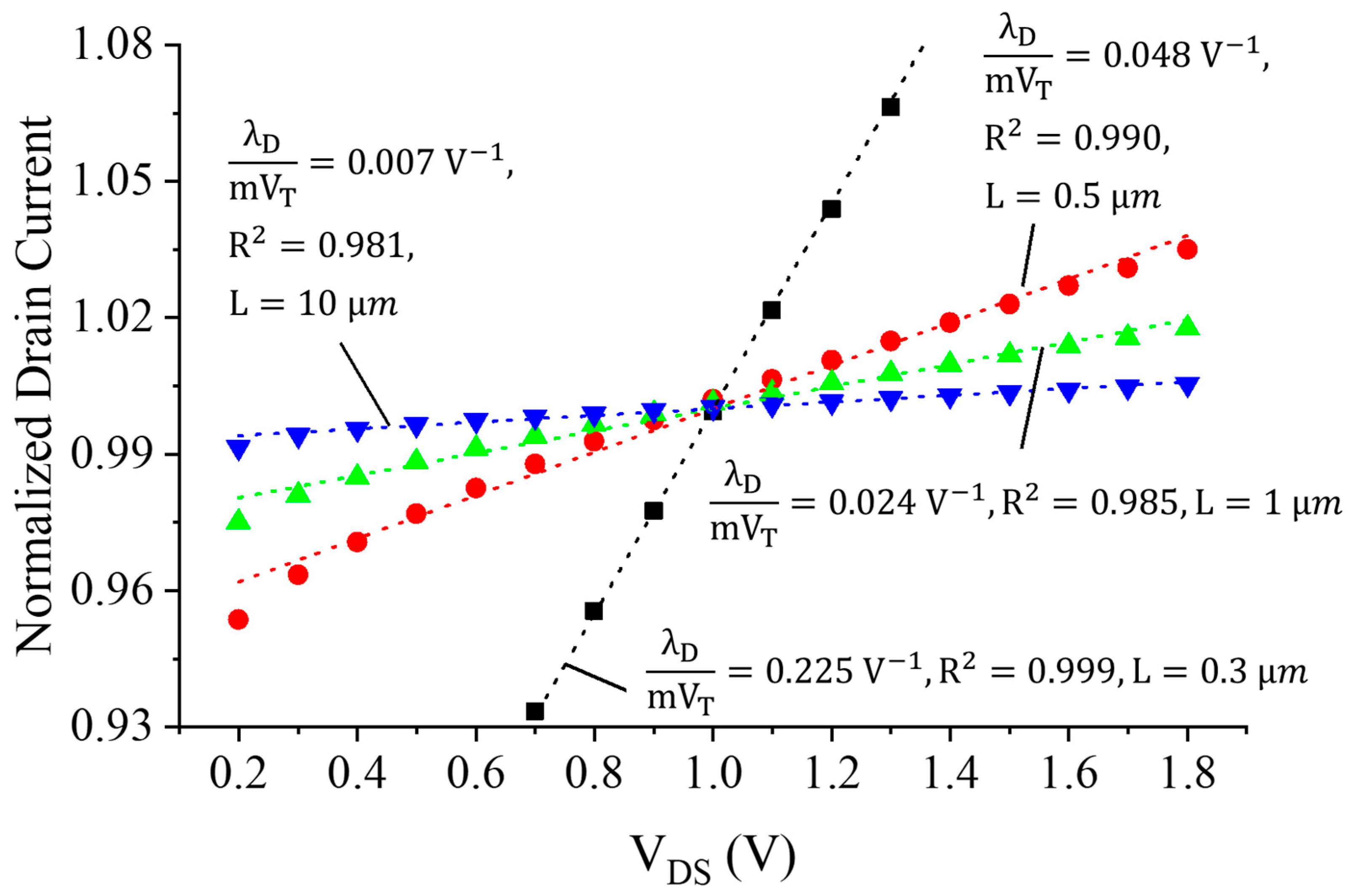
2. DIBL Effect
3. Design and Analysis
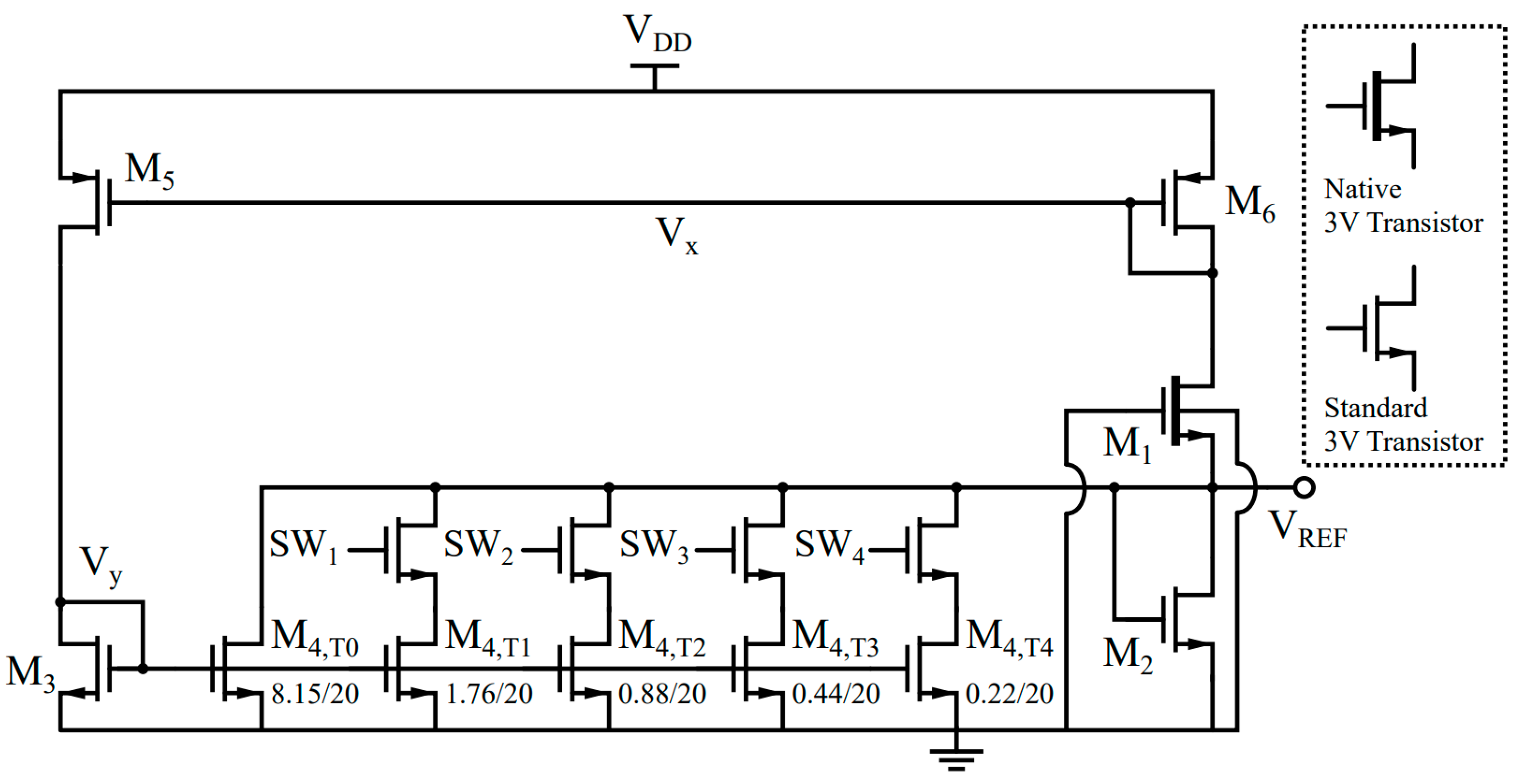
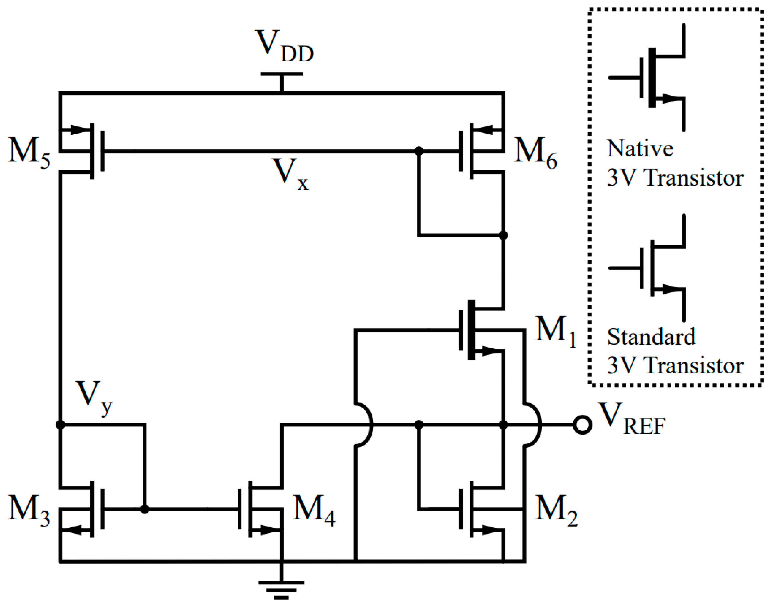
3.1. Circuit Description
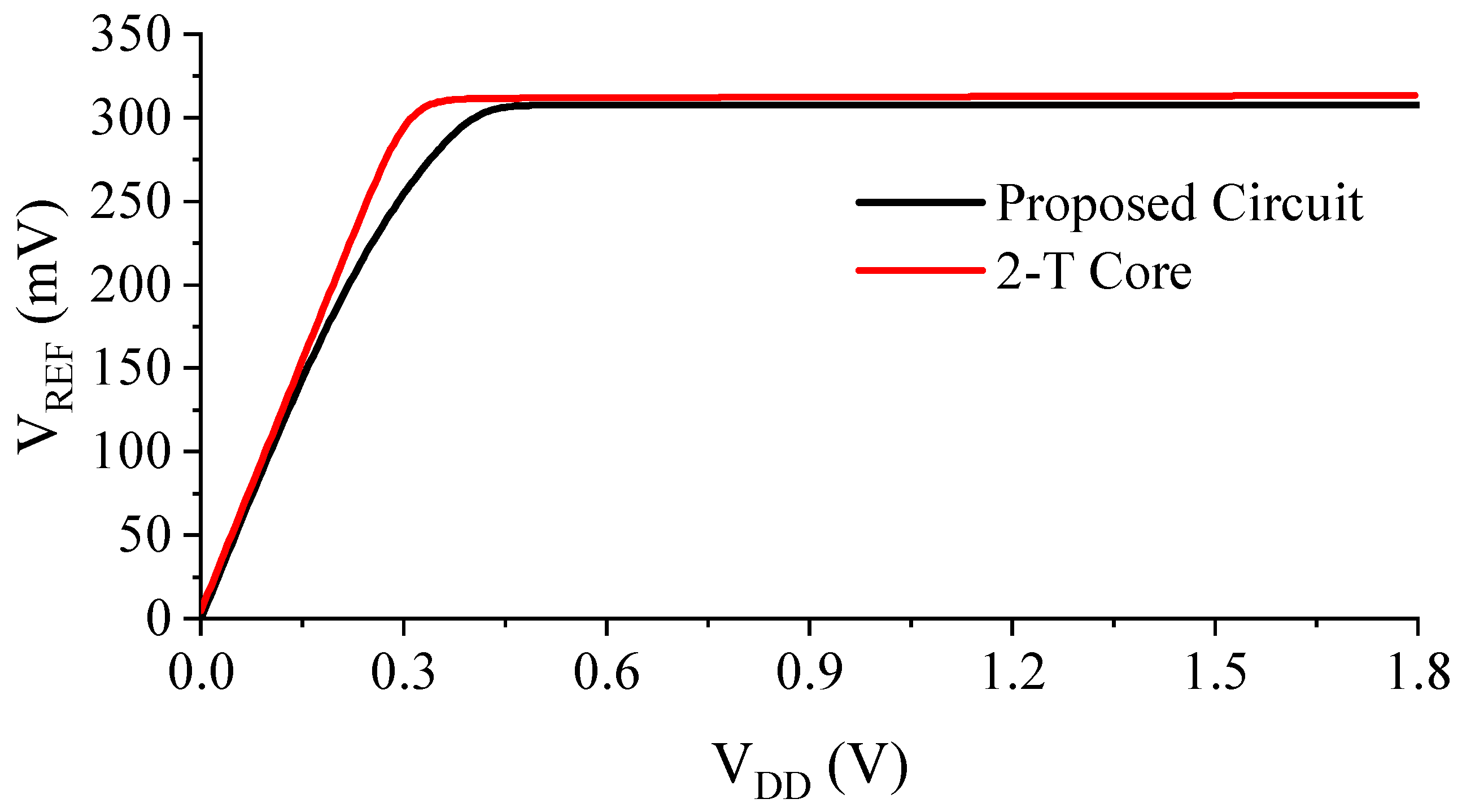
3.2. Minimum Supply Voltage
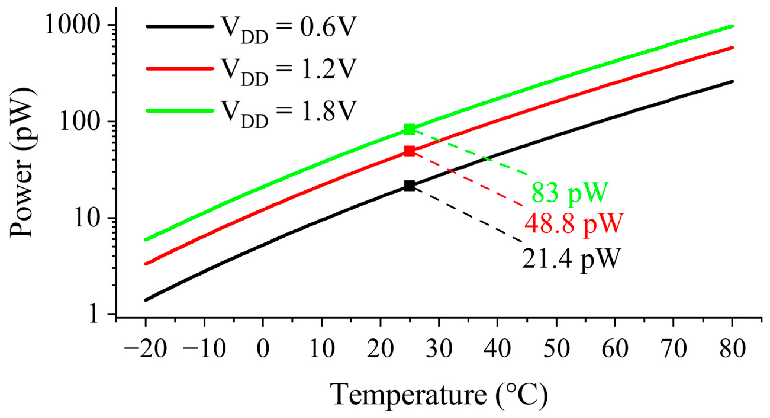
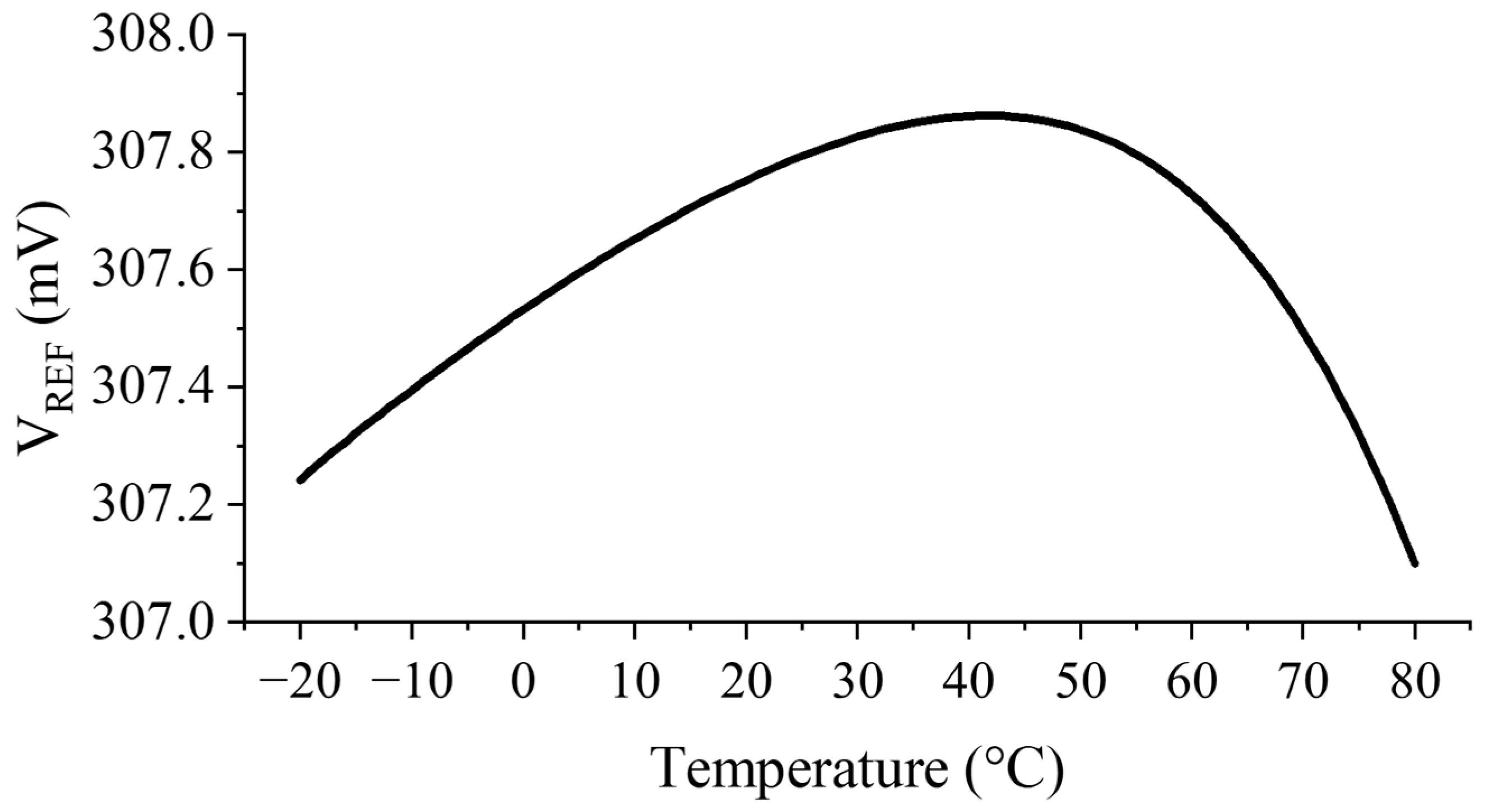
3.3. Temperature Coefficient
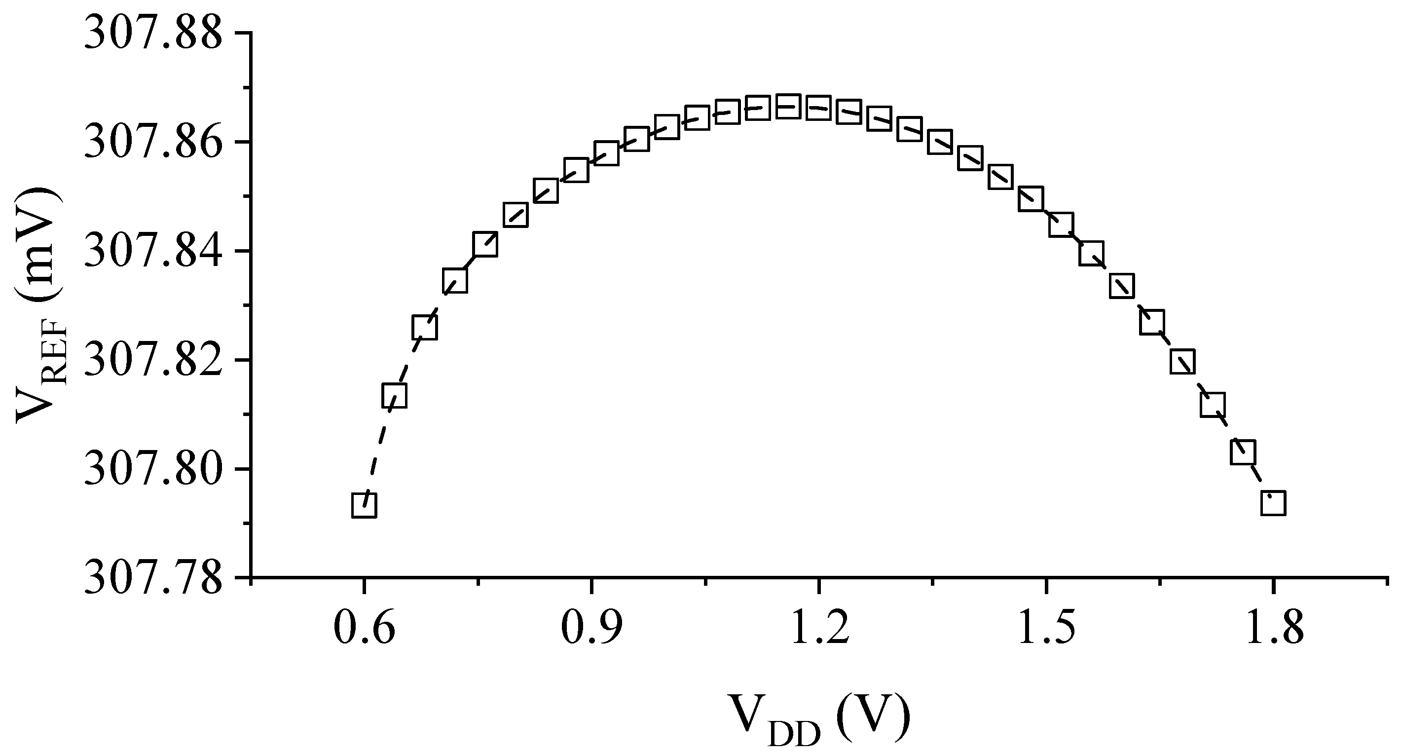
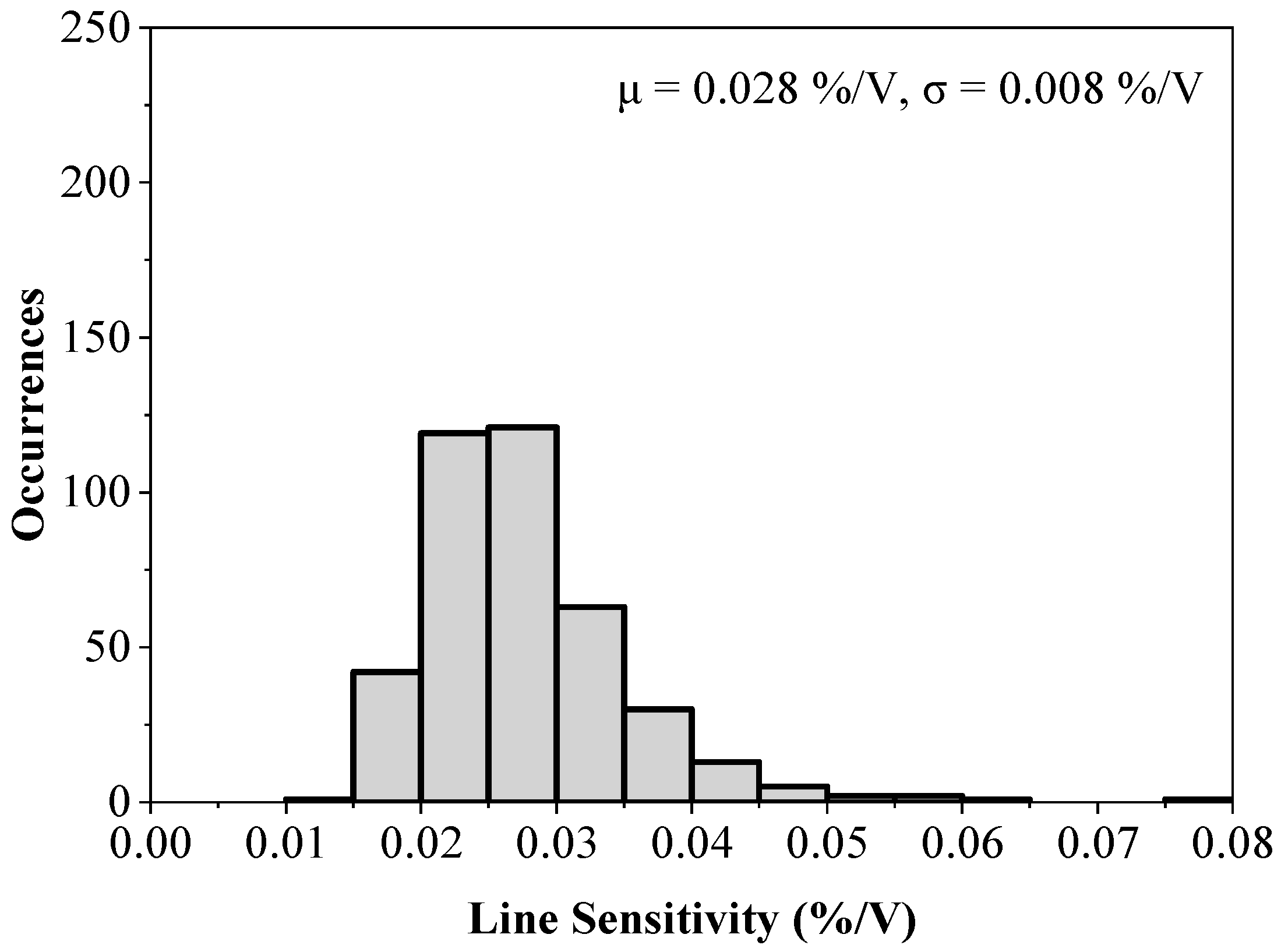
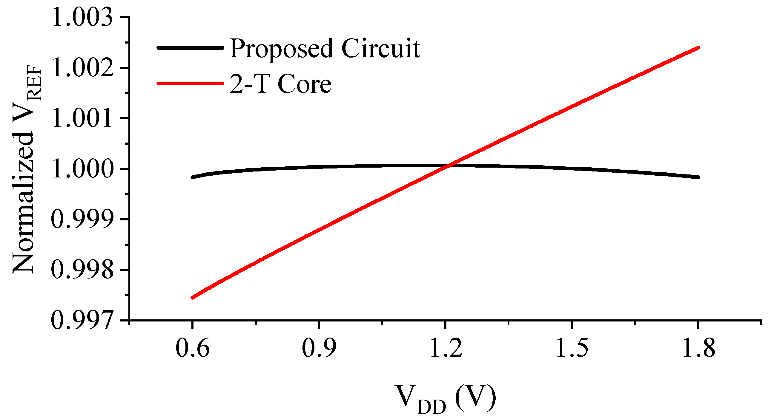
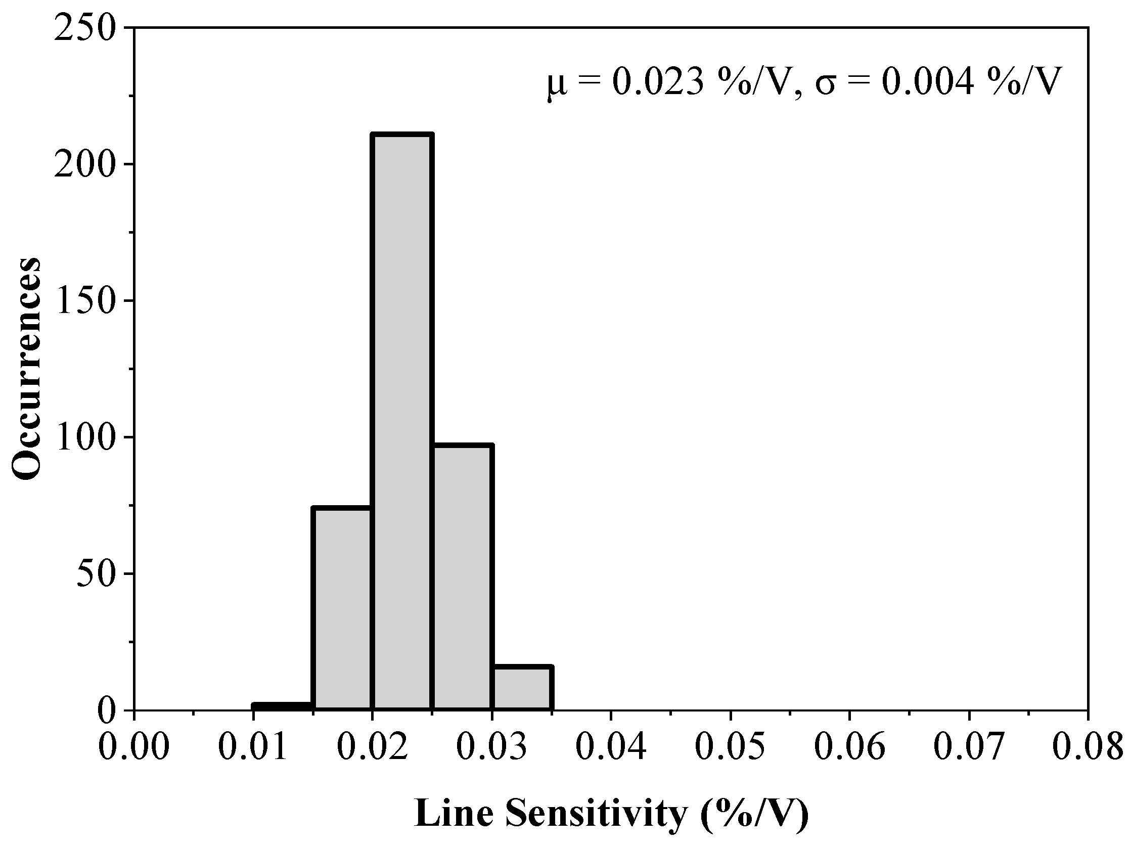
3.4. Line Sensitivity
3.5. Line Sensitivity
4. Design Methodology
- Determining the dimensions of M5 and M6: The current mirroring ratio between M3 and M4 needs to be small () to reduce the DC bias current of M4, so that the output TC is rarely affected by IDS,4. At the same time, to make the supply-dependent current of M4 match with that of M1 while considering such a small mirroring ratio (Figure 3), the length of the PMOS current mirror (M5) needs to be short to create a relatively large supply-dependent current. The width of M6 is found to set and to achieve .
- Determining the optimal dimensions of the 2-T reference: The temperature sensitivity of the proposed circuit is mainly provided by the 2-T reference. M1 and M2 should, thus, be sized to minimize the TC. This step only considers M1, M2 and M6, i.e., M4 is disconnected from the output node. The length of M1 is chosen to be large enough, such that these transistors mitigate the DIBL effect and obtain a better power supply rejection ratio (PSRR). The width of M1 is set by considering the power budget. Finally, the dimension of M2 is found by using the optimum 2-T ratio found in (8) to minimize the TC of VREF.
- Determining the dimensions of M3 and M4: The channel lengths of M3 and M4 should again be chosen to be large enough for better matching. The proper ratio between M3 and M4 determines the LS of the circuit to cancel the DIBL between M1 and M5, as shown in Figure 3.
- Re-optimizing M2 and M4: The additional current of M4 alters the optimum ratio between M1 and M2 found in (8). It is, thus, suggested to slightly re-adjust the size of M2, which in turn might require another change in M4 to also re-optimize for the lowest LS. This optimization loop can be continued until both the TC and LS settle on satisfactory values.
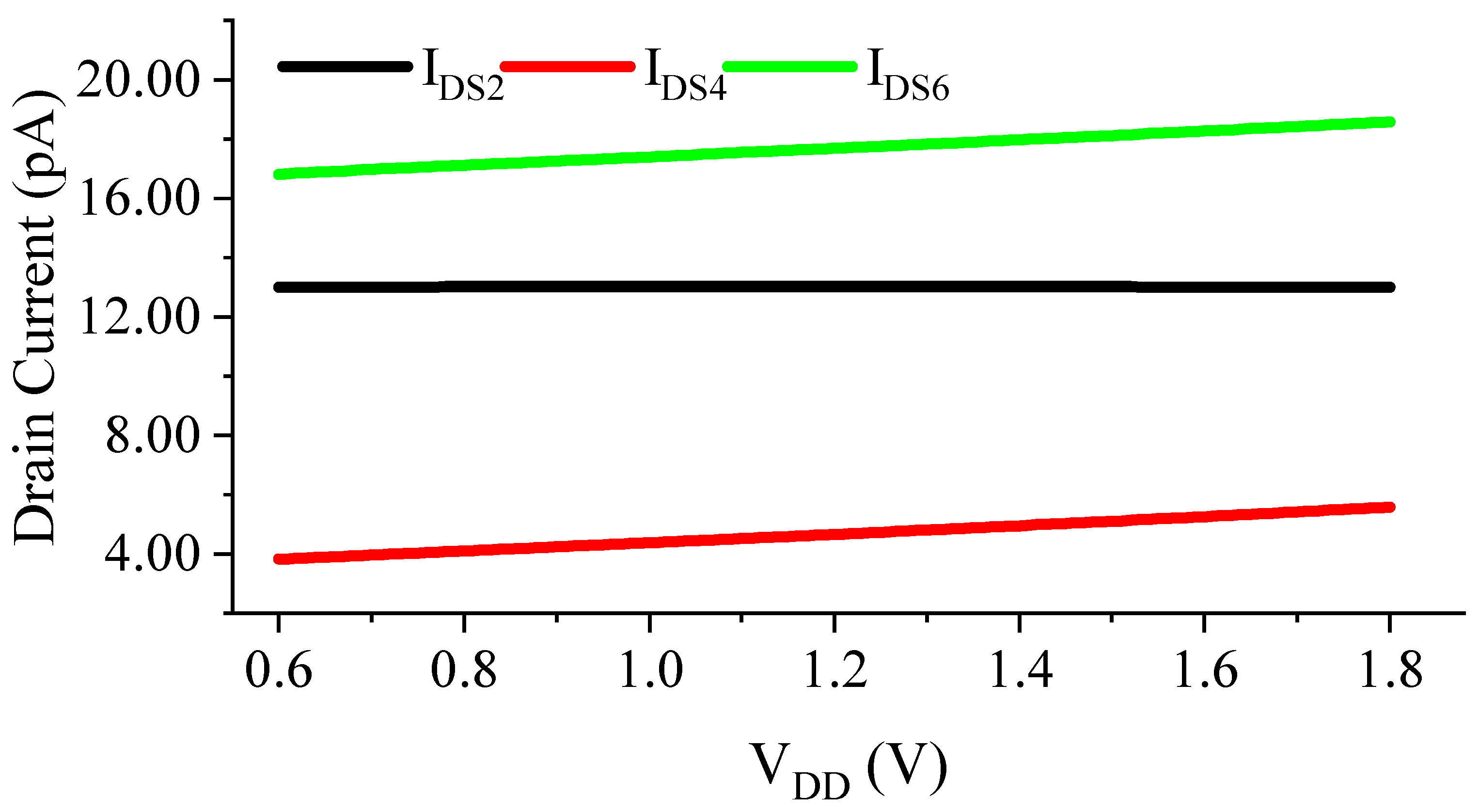
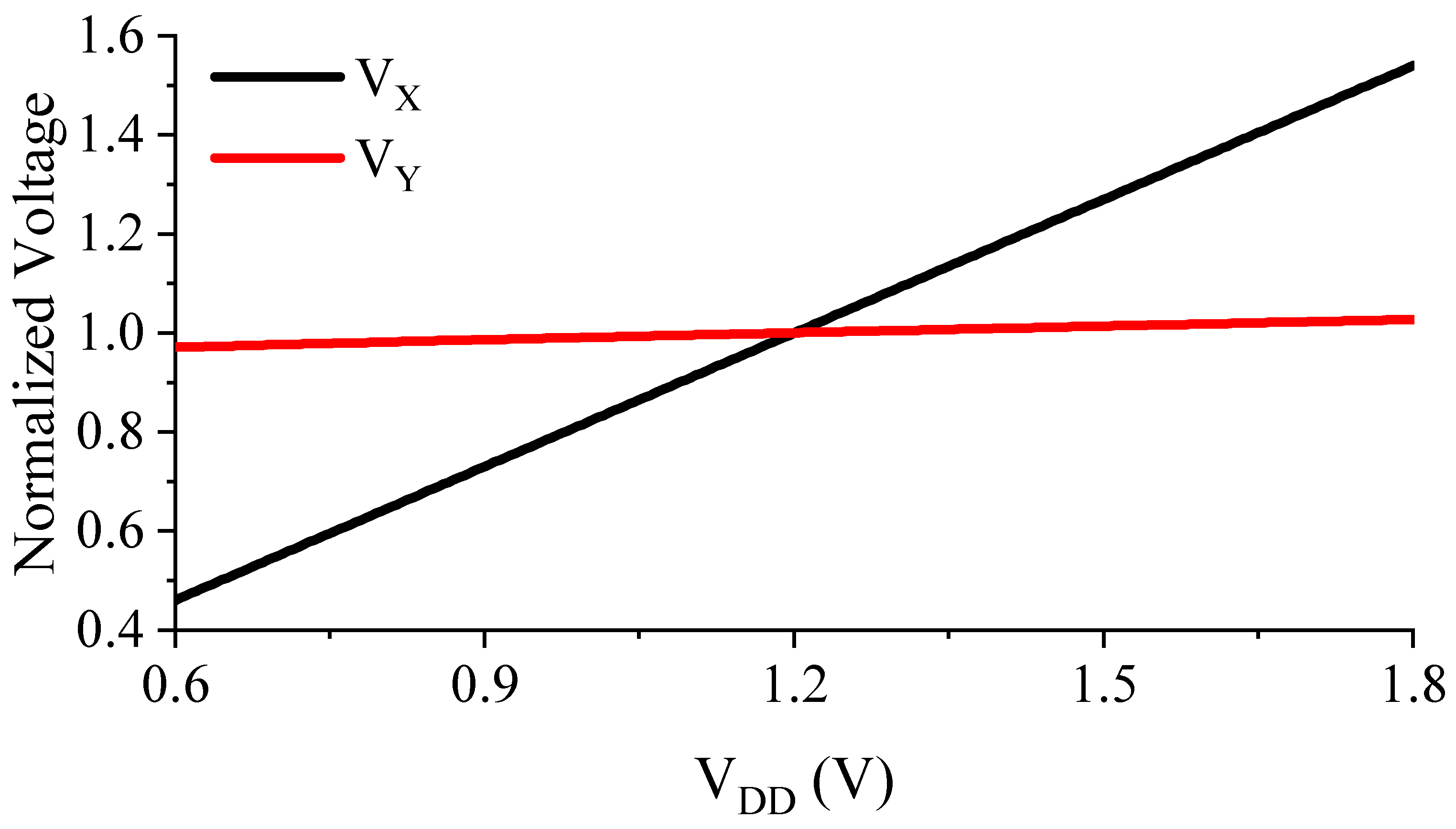
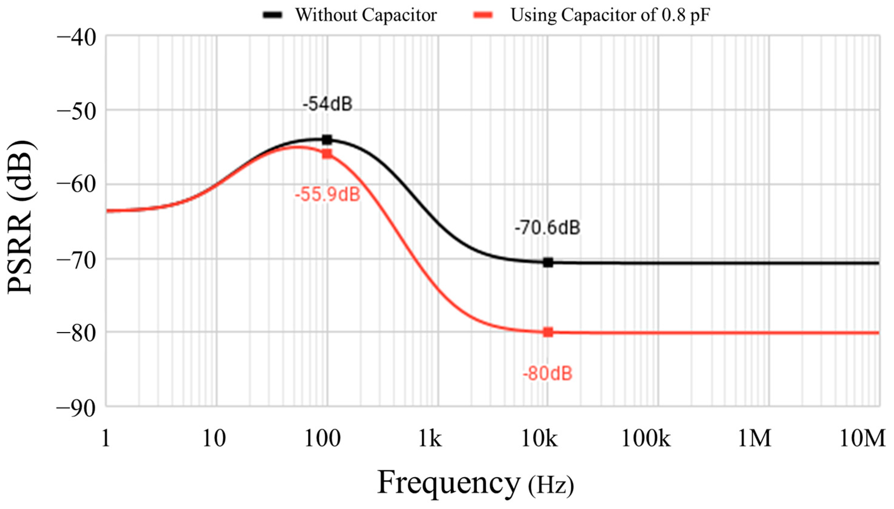
5. Simulation Results
6. Conclusions
Author Contributions
Funding
Institutional Review Board Statement
Informed Consent Statement
Data Availability Statement
Conflicts of Interest
References
- Chen, K.; Petruzzi, L.; Hulfachor, R.; Onabajo, M. A 1.16-V 5.8-to-13.5-ppm/°C Curvature-Compensated CMOS Bandgap Reference Circuit With a Shared Offset-Cancellation Method for Internal Amplifiers. IEEE J. Solid-State Circuits 2021, 56, 267–276. [Google Scholar] [CrossRef]
- Boo, J.-H.; Cho, K.-I.; Kim, H.-J.; Lim, J.-G.; Kwak, Y.-S.; Lee, S.-H.; Ahn, G.-C. A Single-Trim Switched Capacitor CMOS Bandgap Reference With a 3σ Inaccuracy of +0.02%, −0.12% for Battery-Monitoring Applications. IEEE J. Solid-State Circuits 2021, 56, 1197–1206. [Google Scholar] [CrossRef]
- Kim, M.; Cho, S. A Single BJT Bandgap Reference with Frequency Compensation Exploiting Mirror Pole. IEEE J. Solid-State Circuits 2021, 56, 2902–2912. [Google Scholar] [CrossRef]
- Seok, M.; Kim, G.; Blaauw, D.; Sylvester, D. A PorTable 2-Transistor Picowatt Temperature-Compensated Voltage Reference Operating at 0.5 V. IEEE J. Solid-State Circuits 2012, 47, 2534–2545. [Google Scholar] [CrossRef]
- Lin, J.; Wang, L.; Zhan, C.; Lu, Y. A 1-nW Ultra-Low Voltage Subthreshold CMOS Voltage Reference With 0.0154%/V Line Sensitivity. IEEE Trans. Circuits Syst. II Express Briefs 2019, 66, 1653–1657. [Google Scholar] [CrossRef]
- De Oliveira, A.C.; Cordova, D.; Klimach, H.; Bampi, S. Picowatt, 0.45–0.6 V Self-Biased Subthreshold CMOS Voltage Reference. IEEE Trans. Circuits Syst. I Regul. Pap. 2017, 64, 3036–3046. [Google Scholar] [CrossRef]
- Wang, Y.; Sun, Q.; Luo, H.; Wang, X.; Zhang, R.; Zhang, H. A 48 pW, 0.34 V, 0.019%/V Line Sensitivity Self-Biased Subthreshold Voltage Reference With DIBL Effect Compensation. IEEE Trans. Circuits Syst. I Regul. Pap. 2020, 67, 611–621. [Google Scholar] [CrossRef]
- Lee, I.; Sylvester, D.; Blaauw, D. A Subthreshold Voltage Reference With Scalable Output Voltage for Low-Power IoT Systems. IEEE J. Solid-State Circuits 2017, 52, 1443–1449. [Google Scholar] [CrossRef]
- De Oliveira, A.C.; Cordova, D.; Klimach, H.; Bampi, S. A 0.12–0.4 V, Versatile 3-Transistor CMOS Voltage Reference for Ultra-Low Power Systems. IEEE Trans. Circuits Syst. I Regul. Pap. 2018, 65, 3790–3799. [Google Scholar] [CrossRef]
- Qing, D.; Kaiyuan, Y.; Blaauw, D.; Sylvester, D. A 114-pW PMOS-only, trim-free voltage reference with 0.26% within-wafer inaccuracy for nW systems. In Proceedings of the 2016 IEEE Symposium on VLSI Circuits (VLSI-Circuits), Honolulu, HI, USA, 15–17 June 2016; pp. 1–2. [Google Scholar]
- Mu, S.; Chan, P.K. Design of Precision-Aware Subthreshold-Based MOSFET Voltage Reference. Sensors 2022, 22, 9466. [Google Scholar] [CrossRef] [PubMed]
- Shao, C.-Z.; Kuo, S.-C.; Liao, Y.-T. A 1.8-nW, −73.5-dB PSRR, 0.2-ms Startup Time, CMOS Voltage Reference With Self-Biased Feedback and Capacitively Coupled Schemes. IEEE J. Solid-State Circuits 2021, 56, 1795–1804. [Google Scholar] [CrossRef]
- Fassio, L.; Lin, L.; De Rose, R.; Lanuzza, M.; Crupi, F.; Alioto, M. Trimming-Less Voltage Reference for Highly Uncertain Harvesting Down to 0.25 V, 5.4 pW. IEEE J. Solid-State Circuits 2021, 56, 3134–3144. [Google Scholar] [CrossRef]
- Wang, H.; Mercier, P.P. A 420 fW self-regulated 3T voltage reference generator achieving 0.47%/V line regulation from 0.4-to-1.2 V. In Proceedings of the 2017 IEEE European Solid State Circuits Conference (ESSCIRC), Leuven, Belgium, 11–14 September 2017; pp. 15–18. [Google Scholar]
- Grotjohn, T.; Hoefflinger, B. A parametric short-channel MOS transistor model for subthreshold and strong inversion current. IEEE J. Solid-State Circuits 1984, 19, 100–112. [Google Scholar] [CrossRef]


| Transistor | Width (µm) | Length (µm) | Current (pA) |
|---|---|---|---|
| M1 (Native) | 3.2 | 20 | 17 |
| M2 | 10.2 | 20 | 13 |
| M3 | 50 | 20 | 19 |
| M4 | 9.91 | 20 | 4 |
| M5 | 100 | 0.3 | 19 |
| M6 | 100 | 0.3 | 17 |
| This Work * | [4] | [5] | [6] | [7] | [8] | [9] | [10] | [11] | [12] | [13] | [14] | |
|---|---|---|---|---|---|---|---|---|---|---|---|---|
| Technology (nm) | 180 | 180 | 180 | 180 | 180 | 180 | 130 | 180 | 40 | 180 | 180 | 65 |
| VDD (V) | 0.6~1.8 | 0.5~3.6 | 0.4~1.8 | 0.45~3.3 | 0.34~1.8 | 1.4~3.6 | 0.3~1.2 | 1.2~2.2 | 1.2~1.8 | 0.9~1.8 | 0.25~1.8 | 0.4~1.2 |
| VREF (V) | 0.3078 | 0.3284 | 0.151 | 0.2566 | 0.1479 | 1.25 | 0.026 | 0.9862 | 0.8 | 0.261 | 0.094 | 0.3428 |
| Temp. Range (°C) | −20~80 | −20~80 | −40~125 | 0~120 | 0~100 | 0~100 | −25~125 | −40~85 | −40~90 | −40~130 | 0~120 | −40~60 |
| TC (ppm/°C) | 24.8 | 115.3 | 89.83 | 72.4 | 14.8 | 31 | 208 | 86 | 3 | 62 | 265 | 252.2 |
| LS (%/V) | 0.020 | 0.044 | 0.163 | 0.15 | 0.019 | 0.31 | 0.188 | 0.38 | 0.028 | 0.013 | 0.16 | 0.47 |
| Worst LS (%/V) | 0.035 | N/A | N/A | N/A | 0.039 * | N/A | N/A | N/A | N/A | N/A | 0.31 | N/A |
| # of Samples | 400 | 14 | 16 | 5 | 39 400 * | 60 | 5 | 60 | 200 | 15 | 30 | 38 |
| PSRR @ 100 Hz (dB) | −54 | −49 | −55 | −43.9 | −63 | −41 | −67.3 * | −42 | −71.7 | −73.5 | −70 | N/A |
| Power @ 25 °C (pW) | 21.4 | 5.5 | 1000 | 147 | 48 | 33.6 | 40 | 114 | 9600000 | 1800 | 5.4 | 0.42 @ 20 °C |
| Area (mm2) | 0.003 | 0.001425 | 0.005 | 0.002 | 0.0332 | 0.0025 | 0.0006 | 0.00488 | N/A | 0.0059 | 0.0022 | 0.00010 |
Disclaimer/Publisher’s Note: The statements, opinions and data contained in all publications are solely those of the individual author(s) and contributor(s) and not of MDPI and/or the editor(s). MDPI and/or the editor(s) disclaim responsibility for any injury to people or property resulting from any ideas, methods, instructions or products referred to in the content. |
© 2023 by the authors. Licensee MDPI, Basel, Switzerland. This article is an open access article distributed under the terms and conditions of the Creative Commons Attribution (CC BY) license (https://creativecommons.org/licenses/by/4.0/).
Share and Cite
Colbach, L.; Jang, T.; Ji, Y. A 21.4 pW Subthreshold Voltage Reference with 0.020 %/V Line Sensitivity Using DIBL Compensation. Sensors 2023, 23, 1862. https://doi.org/10.3390/s23041862
Colbach L, Jang T, Ji Y. A 21.4 pW Subthreshold Voltage Reference with 0.020 %/V Line Sensitivity Using DIBL Compensation. Sensors. 2023; 23(4):1862. https://doi.org/10.3390/s23041862
Chicago/Turabian StyleColbach, Louis, Taekwang Jang, and Youngwoo Ji. 2023. "A 21.4 pW Subthreshold Voltage Reference with 0.020 %/V Line Sensitivity Using DIBL Compensation" Sensors 23, no. 4: 1862. https://doi.org/10.3390/s23041862
APA StyleColbach, L., Jang, T., & Ji, Y. (2023). A 21.4 pW Subthreshold Voltage Reference with 0.020 %/V Line Sensitivity Using DIBL Compensation. Sensors, 23(4), 1862. https://doi.org/10.3390/s23041862