Communication

Design of Low-Noise CMOS Image Sensor Using a Hybrid-Correlated Multiple Sampling Technique

Department of Semiconductor Science, Dongguk University, Seoul 04620, Republic of Korea
*
Author to whom correspondence should be addressed.
Sensors 2023, 23(23), 9551; https://doi.org/10.3390/s23239551
Submission received: 26 October 2023 / Revised: 25 November 2023 / Accepted: 30 November 2023 / Published: 1 December 2023
(This article belongs to the Special Issue Integrated Circuits and CMOS Sensors)

Abstract

:
We present a 320 × 240 CMOS image sensor (CIS) using the proposed hybrid-correlated multiple sampling (HMS) technique with an adaptive dual-gain analog-to-digital converter (ADC). The proposed HMS improves the noise characteristics under low illumination by adjusting the ADC gain according to the incident light on the pixels. Depending on whether it is less than or greater than 1/4 of the full output voltage range from pixels, either correlated multiple sampling or conventional-correlated double sampling (CDS) is used with different slopes of the ramping signals. The proposed CIS achieves 11-bit resolution of the ADC using an up-down counter that controls the LSB depending on the ramping signals used. The sensor was fabricated using a 0.11 μm CIS process, and the total chip area was 2.55 mm × 4.3 mm. Compared to the conventional CDS, the measurement results showed that the maximum dark random noise was reduced by 26.7% with the proposed HMS, and the maximum figure of merit was improved by 49.1%. The total power consumption was 5.1 mW at 19 frames per second with analog, pixel, and digital supply voltages of 3.3 V, 3.3 V, and 1.5 V, respectively.

1. Introduction

As various technologies, such as the Internet of Things (IoT) and self-driving cars, have developed, CMOS image sensors (CISs) go beyond the role of sensing on behalf of the human eye and require the ability to recognize objects, even in situations where it is difficult to observe them with the human eye [1,2,3]. To this end, various circuit techniques have been proposed to obtain high-quality images by increasing the dynamic range or reducing dark random noise (DRN) [4,5,6]. In general, CIS uses a correlated double sampling (CDS) technique to reduce readout noise by sampling the output voltages of the pixel twice. A correlated multiple sampling (CMS) technique that repeats the CDS process several times has been proposed to reduce DRN [7,8,9,10]. Figure 1a,b show the analog-to-digital converter (ADC) conversion periods during signal sampling when using CDS and CMS, respectively. The CMS repeats the ADC m times to obtain m times more digital output code than the conventional CDS technique. DRN can be reduced by averaging the output code. However, as shown in Figure 1b, the CMS technique repeats the ADC time several times (twice in Figure 1b), which increases the 1-H(horizontal) time and ultimately reduces the frame rate per second (FPS). To solve this problem, a pseudo-CMS (PMS) that maintains the ADC time and adjusts the analog gains by adjusting the slopes of the ramping signals was proposed, as shown in Figure 1c [11]. When the ramping slope for conventional CDS operation is S, the slope of PMS, SPMS, is 2S (analog gain = 1/2Χ), and the output code is half that of Figure 1a. To obtain the same output code, the counter clock frequency CNT_CLK should be doubled. However, PMS uses the same CNT_CLK as CDS and adds the number of counting clocks during the up and down operations to obtain the same output code as the CDS technique. In the case of PMS, to generate odd output codes, the maximum voltage of the slope in the upward direction should be VRMP-VLSB, resulting in a difference in the up- and down-ramping slopes. In addition, because the PMS technique lowers the analog gain, which lowers the ADC resolution by one bit, the quantization noise of the ADC increases. Therefore, to maintain ADC resolution, a high-speed CNT_CLK as high as a multiple of the analog gain is required for a dual-gain-based ramp ADC [12].
Figure 1d shows the proposed hybrid-correlated multiple sampling (HMS) technique, which divides the CMS and CDS sections according to illumination. While reducing the DRN with CMS under low illumination, the FPS can be increased under high illumination, which requires a long ADC time by adjusting the analog gain with conventional CDS, called an adaptive dual-gain ADC. When the input is divided into four parts, under low illumination (1/4 of the input), the CMS ramping signal (VRMP1) goes down and up only at the 1/4 point. The slope, SHML,L, is S, and the output code is the same as that in Figure 1a. If the input was greater than 1/4, VRMP2 was used. When using VRMP2, the ramping start voltage of VRMP2 is lower than that of VRMP1 by 1/4 of ΔVIN (=VRES − VSIG), and SHMS,M is 2S. Unlike [12], a double data rate (DDR) structure is used instead of using 2Χ higher fCNT_CLK, leading to the use of CNT_CLK for all operations. Finally, 1/4 of the input part (under high illumination) used the same CNT_CLK and S to achieve a linear ADC transfer curve. Therefore, the HMS proposed for a low-noise CIS operates faster than the techniques mentioned without high-frequency clocks.
Figure 2 compares the detailed SS-ADC timing diagrams of the conventional CMS and the proposed HMS. The CMS shown in Figure 2 requires two sampling times and an ADC time of 6144 clks, which is 2.4 times longer than that of the regular CDS (tADC = 2560 clk). CMS is performed to reduce the DRN by twice the ADC time. The proposed single-slope ADC (SS-ADC) with an HMS is identical to the existing SS-ADC structure, except for the ramp generator. For HMS operation, two different ramping slopes (VRMP1 and VRMP2) in the low- and high-illuminance ranges are required. Specifically, 0–1/4 of ΔVIN (low-illuminance range), VRMP1 with a doubled analog gain is used; 1/4–3/4 of ΔVIN (middle-illuminance range), VRMP2 with an analog gain is used; and in 3/4–1 of ΔVIN (high illuminance range), VRMP2 with a doubled analog gain is used to achieve low noise and high frame rates.
Therefore, the proposed CIS with HMS reduces low-illumination noise through CMS and increases the FPS by adjusting the analog/digital gains. The CMS in this study was implemented through 1-bit shifting after removing the LSB without the additional circuit required by the existing CMS. In addition, the D-CDS time can be reduced without a higher counter-clock frequency with a double data rate (DDR). The remainder of this paper is organized as follows. In Section 2, we describe the detailed operation and implementation of the CIS structure using the proposed HMS. Section 3 presents the measurement results. Finally, the conclusions are presented in Section 4.

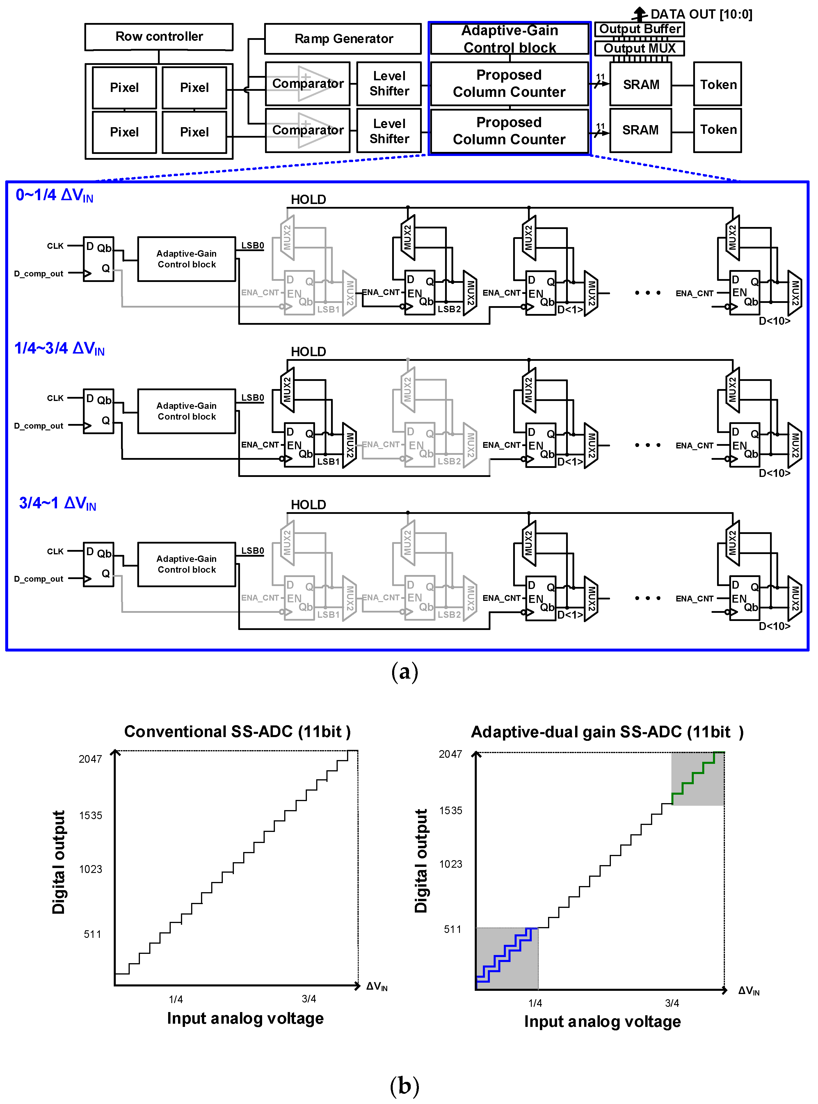
2. Proposed CIS Structure

Figure 3 shows the proposed CIS consisting of an image resolution of 320 × 240 pixels and an 11-bit column-parallel SS-ADC structure using CMS under low illumination and CDS with adaptive-dual gain in middle/high-illumination conditions. The prototype sensor consisted of a pixel array, an 11-bit column counter for the HMS, a ramp-select circuit using feedback to separate low and high incident light levels, and other digital peripheral blocks. In addition, the readout circuit of each column consisted of a comparator, 11-bit two-stage static random-access memory (SRAM), and a column decoder for H-scanning. A two-stage SRAM allows for simultaneous input from the first stage while outputting values from the second stage. Using second-stage SRAM, the frame rate can be increased by using a pipelining readout that overlaps the sampling and readout periods of the row that receives light from the pixel.

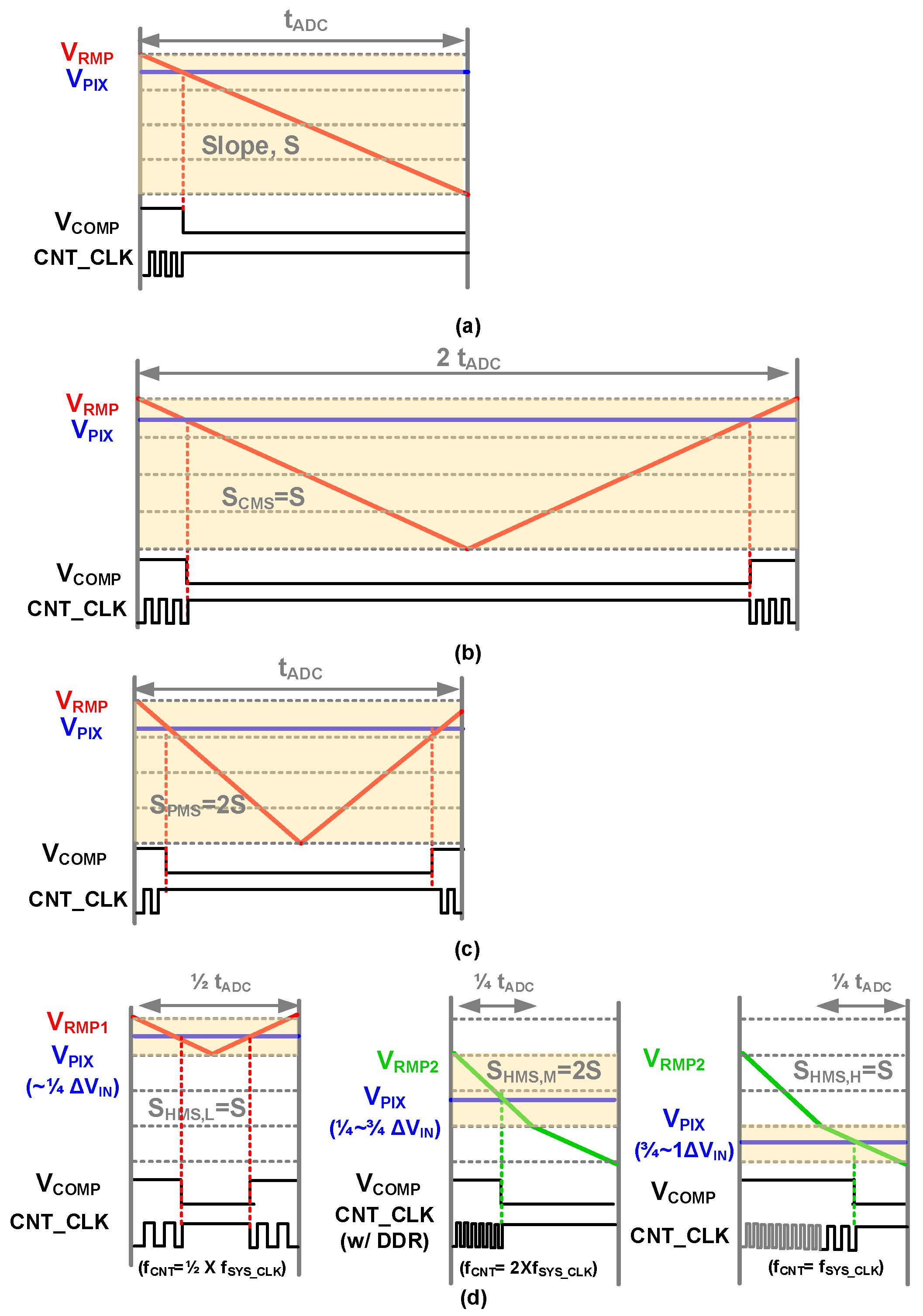
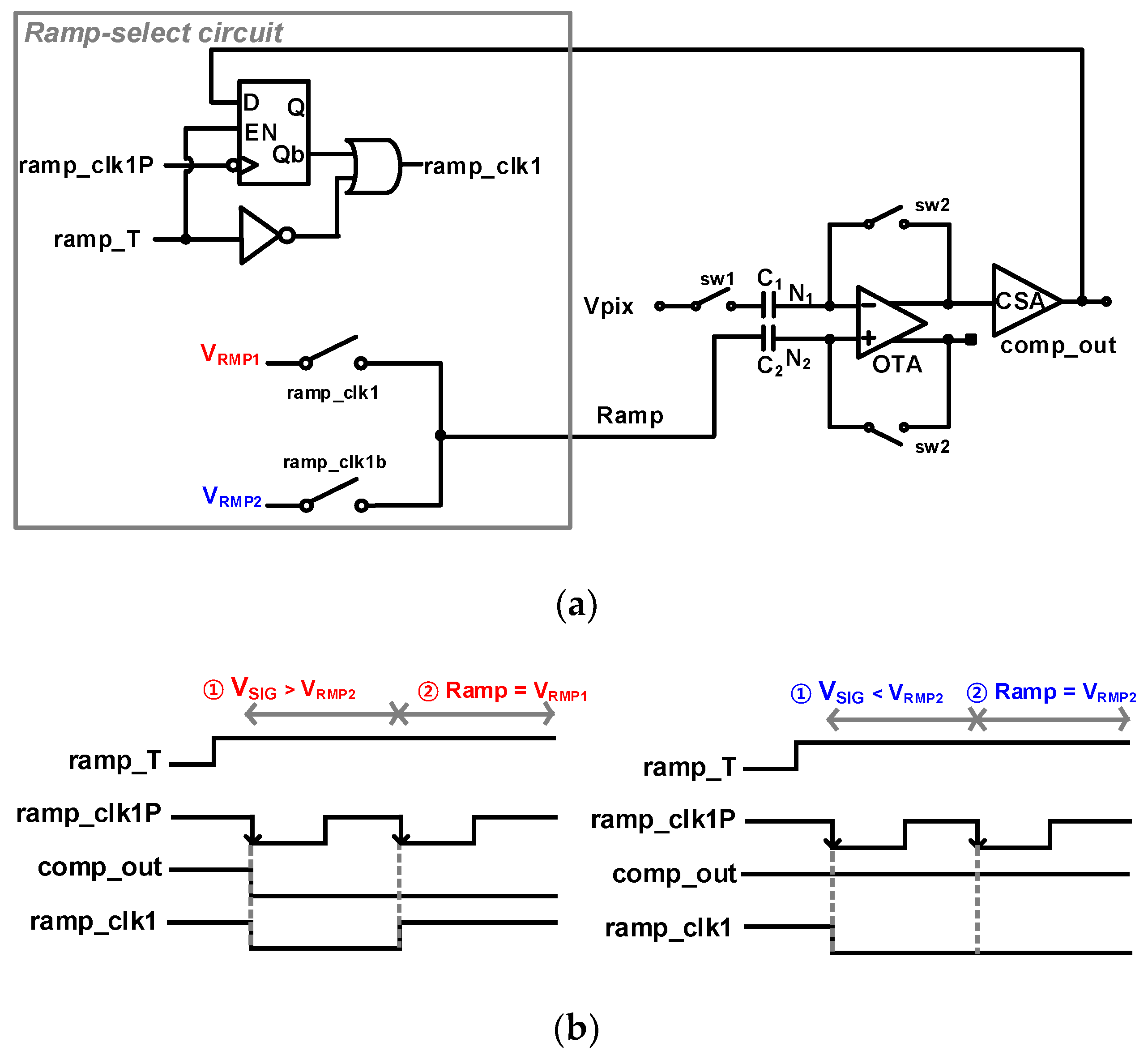
2.1. Ramp-Select Circuit Using Feedback Scheme

Unlike the existing CIS read-out method, it operates as a CMS under low light and CDS under high light; therefore, each of the two ramp signals must be appropriately selected. For this purpose, a ramp-select circuit was proposed and integrated into a conventional digital CDS (D-CDS) structure. Figure 4a shows a block diagram of a ramp–select circuit using D-CDS. For a four-transistor pixel, the reset voltage, VRES, is sampled first, followed by the signal voltage, VSIG. After auto-zeroing using C1 and C2, VSIG and VRMP2 are sampled to compare which voltage is higher, and then the ramping signal is selected. With the proper ramping signal, the D-CDS for VSIG sampling was performed. The period for selecting the ramping signals begins when the ramp_T signal in Figure 4b becomes ‘H’. When the negative-edge-triggered D flip-flop (N-ETDFF) is enabled by ramp_T, VRMP2 and VSIG with 1/4 of ΔVIN (=VRES − VSIG) enter the input of the comparator, VPIX. Ramp_clk1P is the same as the system clock used for the ramp-select period between the reset and signal sampling periods. If the light entering the pixel has low illumination between 0 and 1/4 of ΔVIN, VSIG is higher than VRMP2, and comp_out becomes ‘L’. The comparator output was fed back into the input of the N-ETDFF of the ramp-select circuit. When the second falling edge of ramp_clk1P occurs, ramp_clk1 becomes ‘H’ by the feedback comparator output, and VRMP1 is selected for the CMS operation. On the other hand, when the light entering the pixel is 1/4 to 1 of ΔVIN, VRMP2 is higher than VSIG, so comp_out is ‘H’. Therefore, the second falling edge of ramp_clk1P makes ramp_clk1 ‘L’, and VRMP2 is selected for the CDS operation.

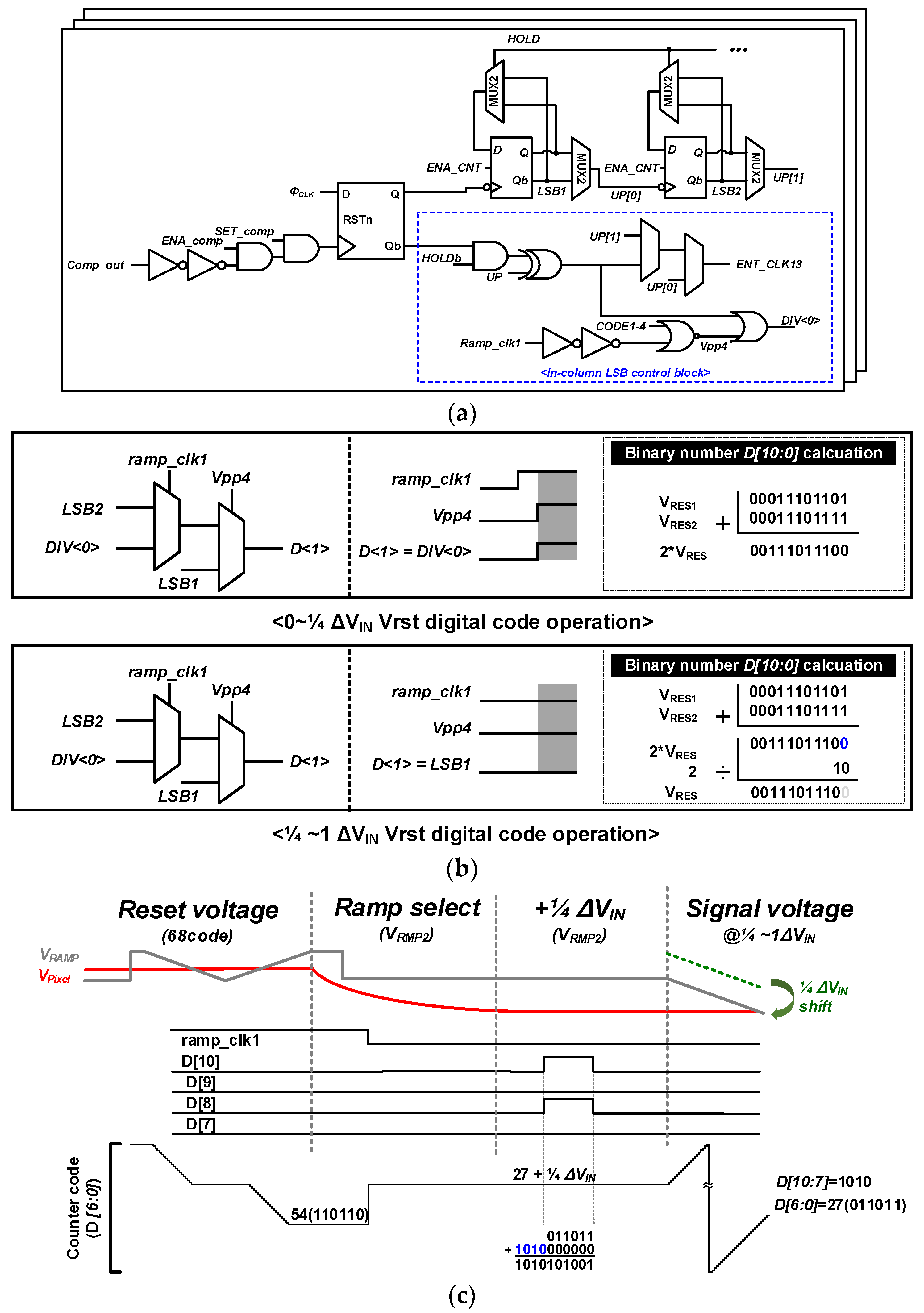
2.2. Binary Calculation for HMS

Unlike 1/4 to 1 of ΔVIN, which outputs a digital code according to the illuminance as is through single sampling, it requires sampling twice to reduce noise in low illuminance and calculates twice the digital code output. In the case of the existing CMS, an additional calculation circuit for m times digital code output is required when multi-sampling m times, but this can be calculated by adjusting the LSB owing to the nature of the digital code of binary numbers. During CMS operation under low illumination conditions, removing D<0>, which corresponds to the LSB of the digital code output twice, and shifting all bits from D<N> to D<N-1> is equivalent to dividing by two. Therefore, the digital code expressed in binary numbers can be outputted by dividing the double digital code by two by deleting the LSB and then shifting the code toward the LSB. Figure 5 shows two examples. For the even output codes, if the signal code for the first sampling is 237 and the signal code for the second sampling is 239, which is 237 + 239 = 476 code, the final output should be 476/2 = 238 code. As shown in Figure 5a, if we delete 0 corresponding to the LSB of the code corresponding to 476 and shift it, it is the same as the binary digital code corresponding to 238. Figure 5b illustrates the case of odd-output codes. The double digital code included 237 codes for the first sampling and 238 codes for the second sampling. In the case of the 237 + 238 = 475 code, each bit is shifted after discarding the LSB code; therefore, when 475/2 = 237.5, the decimal point is discarded to 237. This is similar to that of the corresponding binary digital code.
Figure 6a,b show the block diagram and operating principle of the column-parallel HMS circuit for controlling the LSB by illuminance in an adaptive-dual gain ADC. The HMS counter uses the conventional up-down counter (UDC) structure and the DIV<0> signal with the same period as the system clock (CLK) of 1 LSB. When the pixel output was less than 1/4 of ΔVIN, the reset voltage was doubled and the reset voltage was sampled twice, as shown in Figure 6b. The LSB clock period DIV<0> was determined through ramp_clk1 and Vpp4 signals using a multiplexer (MUX). When the pixel voltage is 1/4 to 1 of ΔVIN, the reset voltage doubled by VRMP1 must be divided into two before sampling the signal voltage. For this division operation, the LSB of the binary digital code was deleted and the digit was shifted by one place. For example, if the reset voltage is 54(10), which is 110110(2), then it becomes 27(10) which is 11011(2) by deleting and shifting the LSB by 0.
For signal sampling, VRAMP starts from 1/4 of ΔVIN of the pixel voltage. Therefore, unlike conventional UDC, a digital code corresponding to 1/4 of ΔVIN is added. For example, as shown in Figure 6c, if the reset voltage is 8 bits and the signal voltage is 11 bits, then 10100000000(2) should be added. Therefore, 10100000000(2) from 1/4 of ΔVIN and 11011(2) during reset voltage sampling were added, resulting in D [10:0] = 10100011011(2).

2.3. LSB Control Counter

Figure 7a shows a block diagram of the column counter, with unit counters operated for each ΔVIN. It consists of 12-unit counters for an 11-bit column counter, and an LSB is generated from LSB1, LSB2, and D<1>, which determines the digital gain at the three different frequencies. The control signal generated from the adaptive-dual gain control block determines the unit counter such that different digital gains are applied for each ΔVIN range. This maintains the linearity of the ADC using the largest digital gain in a ramping signal with different analog gains at 1/4–3/4 of ΔVIN. Figure 7b compares the linearity of the conventional SS-ADC and adaptive-dual gain ADC. Similar to the conventional SS-ADC, the linearity of the proposed adaptive-dual gain ADC can be obtained in all ranges of ΔVIN.

3. Experiment Results

The prototype chip of the proposed CIS was manufactured using a 0.11 μm process. Figure 8a shows a layout and a photograph of the prototype CIS chip occupying an area of 2.55 mm × 5.24 mm. The measurement environment for the proposed CIS is shown in Figure 8b, and the measurement sequence is as follows. An FPGA board, XEM3050 (Xilinx Spartan-3 FPGA Integration Module, Portland, OR, USA), was used to generate control signals to drive the image sensor on a computer. Using the ISE program, control signals were applied to the designated pins of the image sensor in Verilog. Verilog coding was completed, and the sensor output was sequentially read and confirmed using a computer’s image viewer. Xilinx’s Opal Kelly board was used to drive the FPGA based on the USB interface, and measurements were performed by checking the final image displayed in the image viewer. Figure 8c shows an image measured from the proposed CIS, indicating that all 11-bit codes are output through the ADC using two ramping signals for each illuminance. For the entire code, it was confirmed that the ramping signals were automatically selected according to illuminance.

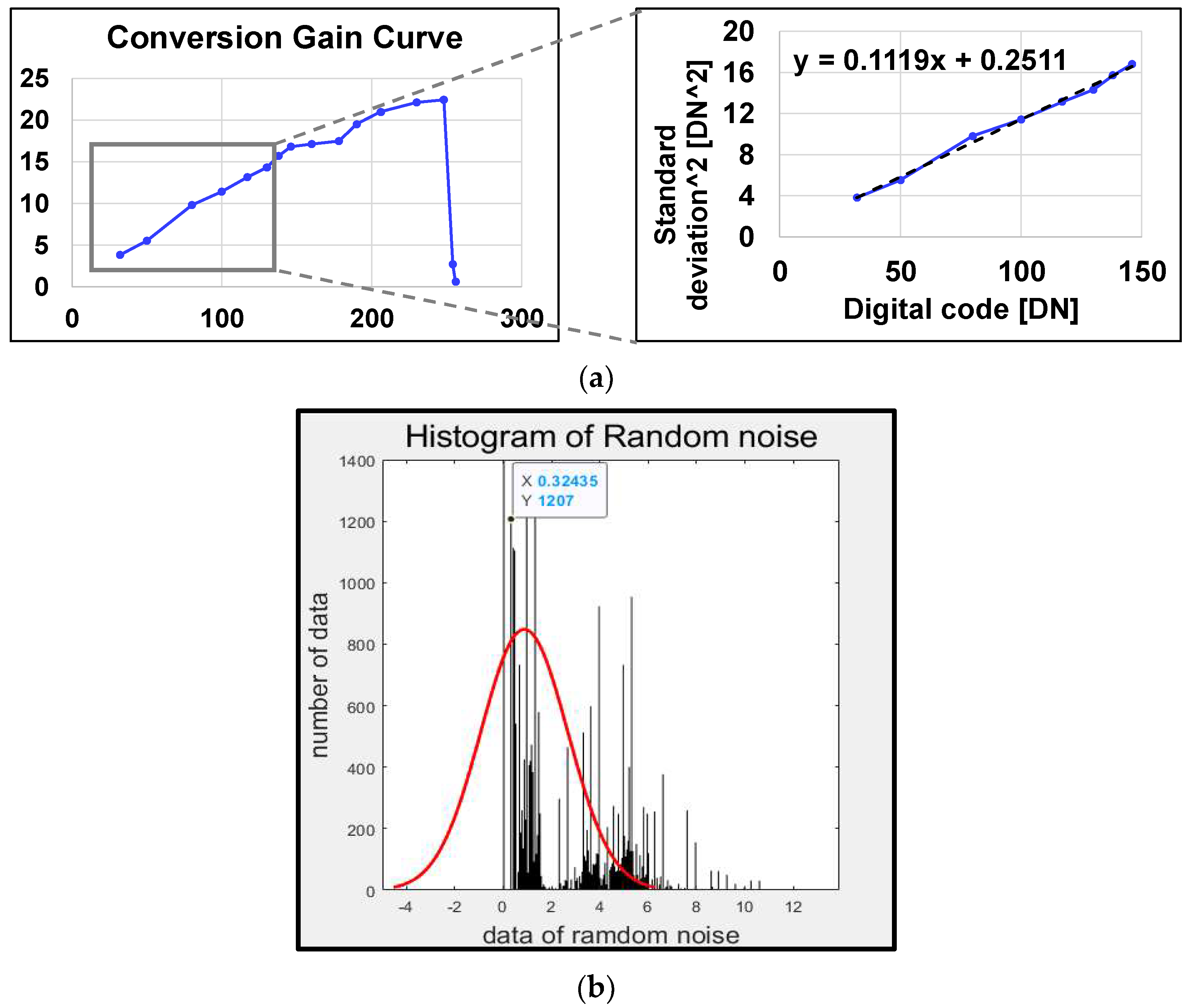
3.1. Dark Random Noise

The relationship between the output code of the ADC that is finally output to calculate the conversion gain (CG) of the image sensor and CG is as follows:
Image   output   level = 1 CG × Incident   photon + Image   offset   signal
The image offset signal is the signal level when no light is incident. In addition, the noise that appears in the image consists of temporal dark noise and shot noise. The equation is as follows:
Total   noise = ( temporal   dark   noise ) 2 + shot   noise 2  
Temporal dark noise occurs when light is not incident; therefore, it can be expressed as a very small constant. The above equation can be summarized as follows:
Total   noise 2 = number   of   photons = CG × output   digital   value
Figure 9 shows the measurement results for CG and DRN. In Figure 9a, CG is linear as DRN increases until the pixel is saturated by photons. Figure 9b shows the slope of the trend line CG = 0.1119 (DN/e) and 43.71 (μV/e), where DN is a digital number. DRN is the noise generated by the readout circuit, which is reflected in the output data and digital number (DN) during ADC measurement. The root-mean-square (RMS) DRN calculates the average DN caused by noise when no light enters a pixel. Because DN uses the standard deviation of the histogram, the image was measured several times and a value close to the average was obtained. Consequently, the RMS DRN of the proposed circuit is RN = 0.32435 (DN) and 2.9 (e rms).

3.2. Signal-to-Noise Ratio

Table 1 shows the signal-to-noise ratio (SNR) of the proposed SS-ADC with an HMS and the existing SS-ADC measured by dividing illuminance into three parts. According to Table 1, the proposed circuit shows a tendency for noise to increase as the light intensity increases. However, the SNR increases as the amount of light increases because the increase in the output digital code is larger. Compared to the existing SS-ADC, it increased by 53.4% at low illuminance and 15.31% at medium illuminance. Because the proposed circuit achieves a noise reduction effect through CMS under low illumination (@0 V~1/4 of ΔVIN), an SNR increase of 38.09% is obtained below 1/4 of ΔVIN.
Table 2 presents a performance comparison of low-noise CISs. Compared to the PMS in [11], the dark random noise in low light was reduced by up to 32% through dual sampling. The proposed CIS has up to 64% lower dark random noise than that in [13], which has low dark random noise with a CMS. In addition, we observed a lower figure of merit (FoM) of 38% at low illumination, corresponding to 0–1/4 of ΔVIN compared to [13].

4. Conclusions

This paper explains the concept and structure of an SS-ADC with a noise reduction effect through CMS in low light, which achieves D-CDS with two ramping signals with different analog/digital gains. The measured image shows that two ramping signals with different ΔVIN values can be applied by automatically detecting the amount of incident light using a ramp-select circuit. The measurement results of the prototype sensor show that image visibility, dark random noise reduction, and SNR are improved through the HMS, especially in low-illuminance areas. As a result, the proposed CIS is expected to be used in various applications such as automotive CIS and object detection.

Author Contributions

S.J.Y. and S.Y.Y. conceived and designed the circuits. H.L., K.J.P., J.K. and S.Y.K. performed the experiments and analyzed the data. All authors have read and agreed to the published version of the manuscript.

Funding

This work was supported in part by National R&D Program through the National Research Foundation of Korea (NRF) funded by Ministry of Science and ICT (2023M3I7A1078936), in part by the Technology Innovation Program (Public-private joint investment semiconductor R&D program(K-CHIPS) to foster high-quality human resources) (RS-2023-00235137) funded by the Ministry of Trade, Industry & Energy (MOTIE, Republic of Korea) (1415187379), and in part by the Dongguk University Research Fund of 2022.

Institutional Review Board Statement

Not applicable.

Informed Consent Statement

Not applicable.

Data Availability Statement

The datasets generated from the current study are available from the corresponding author upon reasonable request.

Acknowledgments

The EDA tool was supported by the IC Design Education Center (IDEC), Republic of Korea.

Conflicts of Interest

The authors declare no conflict of interest.

References

  1. He, Z.; Li, F.; Zuo, P.; Tian, H. Principles and Applications of Resonance Energy Transfer Involving Noble Metallic Nanoparticles. Materials 2023, 16, 3083. [Google Scholar] [CrossRef] [PubMed]
  2. Gao, Z.; Yao, S.; Yang, C.; Xu, J. A Dynamic Range Extension Technique for CMOS Image Sensors with In-Pixel Dual Exposure Synthesis. IEEE Sens. J. 2015, 15, 3265–3273. [Google Scholar] [CrossRef]
  3. Jeong, B.; Lee, J.; Choi, J.; Song, M.; Son, Y.; Kim, S. A 0.57 mW@1 FPS In-Column Analog CNN Processor Integrated Into CMOS Image Sensor. IEEE Access 2023, 11, 61082–61090. [Google Scholar] [CrossRef]
  4. Cho, J.; Choo, H.; Lee, S.; Yoon, S.; Kam, G.; Kim, S. Design of a CMOS Image Sensor with Bi-Directional Gamma-Corrected Digital-Correlated Double Sampling. Sensors 2023, 23, 1031. [Google Scholar] [CrossRef] [PubMed]
  5. Fowler, B.; Liu, C.; Mims, S.; Balicki, J.; Li, W.; Do, H.; Vu, P. Wide Dynamic Range Low Light Level CMOS Image Sensor. In Proceedings of the 2009 International Image Sensor Workshop, Bergen, Norway, 26–28 June 2009; pp. 340–343. [Google Scholar]
  6. Ma, C.; Liu, Y.; Li, Y.; Zhou, Q.; Wang, X.; Chang, Y. A 4-M Pixel High Dynamic Range, Low-Noise CMOS Image Sensor with Low-Power Counting ADC. IEEE Trans. Electron Devices 2017, 64, 3199–3205. [Google Scholar] [CrossRef]
  7. Um, B.Y.; Kim, J.R.; Kim, S.H.; Lee, J.H.; Cheon, J.; Choi, J.; Chun, J.H. Design and evaluation of a CMOS image sensor with dual-CDS and column-parallel SS-ADCs. J. Semicond. Technol. Sci. 2017, 17, 110–119. [Google Scholar] [CrossRef]
  8. Cho, K.; Kim, D.; Song, M. A low power dual CDS for a column-parallel CMOS image sensor. J. Semicond. Technol. Sci. 2012, 12, 388–396. [Google Scholar] [CrossRef]
  9. Kawai, N.; Kawahito, S. Effectiveness of a correlated multiple sampling differential average for reducing 1/f noise. IEICE Electron. Exp. 2005, 2, 379–383. [Google Scholar] [CrossRef]
  10. Kawahito, S.; Suh, S.; Shirei, T.; Itoh, S.; Aoyama, S. Noise reduction effects of column-parallel correlated multiple sampling and source-follower driving current switching for CMOS image sensors. In Proceedings of the 2009 International Image Sensor Workshop, Bergen, Norway, 26–28 June 2009; Volume 8. [Google Scholar]
  11. Lim, Y.; Koh, K.; Kim, K.; Yang, H.; Kim, J.; Jeong, Y.; Lee, S.; Lee, H.; Lim, S.H.; Han, Y.; et al. A 1.1 e-temporal noise 1/3.2-inch 8Mpixel CMOS image sensor using pseudo-multiple sampling. In Proceedings of the 2010 IEEE International Solid-State Circuits Conference-(ISSCC), San Francisco, CA, USA, 7–11 February 2010; pp. 396–397. [Google Scholar] [CrossRef]
  12. Xhakoni, A.; Fekri, A.; Francis, P.; Vancauwenbergh, K.; Van Esbroeck, K. A 40000fps global shutter image sensor with 26.7 ns 12-bit row readout time. In Proceedings of the 2021 International Image Sensor Workshop, Online, 20–23 September 2021. [Google Scholar]
  13. Park, H.; Yu, C.; Kim, H.; Roh, Y.; Burm, J. Low Power CMOS Image Sensors Using Two Step Single Slope ADC with Bandwidth-Limited Comparators & Voltage Range Extended Ramp Generator for Battery-Limited Application. IEEE Sens. J. 2020, 20, 2831–2838. [Google Scholar] [CrossRef]
Figure 1. ADC conversion periods of (a) conventional CDS, (b) CMS, (c) pseudo-CMS, and (d) the proposed HMS.
Sensors 23 09551 g001
Figure 2. SS-ADC block diagrams and timing diagrams with CMS and the proposed HMS.
Sensors 23 09551 g002
Figure 3. A full block diagram of the proposed CIS.
Sensors 23 09551 g003
Figure 4. (a) Block diagram and (b) timing diagram of ramp-select circuit. Two timing diagrams are shown with different conditions of VSIG to choose ramping signals between VRMP1 and VRMP2.
Sensors 23 09551 g004
Figure 5. CMS operation for (a) doubled even output codes and (b) doubled odd output codes.
Sensors 23 09551 g005
Figure 6. (a) Block diagram of in-column LSB control block, (b) operation of CMS, and (c) timing diagram of HMS with adaptive-dual gain ADC (1/4 < ΔVIN < 1).
Sensors 23 09551 g006
Figure 7. (a) Block diagram of the column counter and (b) the linearity comparison of conventional and the proposed adaptive-dual gain ADCs (blue line: CMS under low illumination, green line: ×2 using adaptive-dual gain ADC on the right figure).
Sensors 23 09551 g007
Figure 8. (a) A layout and chip microphotograph, (b) test environment, and (c) evaluated images with 2 ramps @ 0 to 1200 luxs.
Sensors 23 09551 g008
Figure 9. (a) Conversion gain graph and (b) DRN calculated with histogram using Matlab.
Sensors 23 09551 g009
Table 1. Measured output (mV), noise (mV), SNR (dB) with different illumination (Lux).
IlluminationOutputNoiseSNRSS-ADC
SNR
34095.402.1832.8021.38
900275.396.1133.0628.68
1280466.648.8734.4228.71
Table 2. Comparison of performance characteristics of the proposed CIS with other works.
[11][13]This Work
Technology (nm)9090110
Image Resolution8 M960 × 720320 × 240
Pixel Size (μm2)1.4 × 1.41.4 × 1.43.25 × 3.25
ADC Column Pitch (μm)2.8 (even/odd readout)2.8 (even/odd readout)3.25 (even readout)
ADC Resolution (bit)1010 11
System CLK (MHz)1305012.5
Random Noise (VRMS)336 μ472 μ80.39 μ
169.69 μ
Total Power (mV)280285.349
FoM
(VRMS·W/FPS·# of Pixels)
N/A542.8 μ @dark336 μ @dark
710.15 μ @bright
Disclaimer/Publisher’s Note: The statements, opinions and data contained in all publications are solely those of the individual author(s) and contributor(s) and not of MDPI and/or the editor(s). MDPI and/or the editor(s) disclaim responsibility for any injury to people or property resulting from any ideas, methods, instructions or products referred to in the content.

