1. Introduction
Modern digital electronics design must operate in energy efficient, low-cost, and resource-constrained environments. Unfortunately, the conventional approaches known in the literature to save power consumption [
1,
2], although acting at the algorithm as well as at the architecture, circuit, and transistor levels, may not be effective enough in such contexts, unless renouncing to very high speeds. In fact, in many cases, state-of-the-art digital circuits are required to accelerate emerging applications, such as data mining and recognition, data analytics, multimedia processing, machine learning, and the Internet of Things (IoT), just to name few [
3,
4], which demand impressive computational capabilities and very high performance levels to process huge amounts of data. However, the error-resilient feature of these applications has afforded promising opportunities to achieve new and even more efficient low-power design approaches. As an example, the approximate computing is known as a powerful technique that relaxes the constraint of an exact computation, in order to trade the quality of the result with speed, area, and energy consumption [
5,
6,
7]. As recently demonstrated in a plethora of papers [
5,
6,
7,
8,
9,
10,
11,
12,
13,
14,
15,
16,
17,
18], employing approximate arithmetic data-paths obviously introduces errors in the performed computations, but allows the computational time, the energy consumption, and the resources requirements to be reduced, thus ensuring a good quality-energy trade-off to be achieved.
As it is well known, additions and multiplications are the basic operations in almost all digital data-paths. Therefore, it is not surprising that the design of approximate adders and multipliers have received a great deal of attention. However, the vast majority of the existing architectures are oriented to the design of Application Specific Integrated Circuits (ASICs) that efficiently exploit low-level techniques based on the gate- and transistor-level circuit modifications [
5,
6,
7,
8,
9,
10,
11,
12,
13,
14,
15]. Unfortunately, these techniques cannot be applied directly to circuit designs based on Field Programmable Gate Arrays (FPGAs). In fact, the unique structure of FPGA devices, consisting of a reduced set of hardware primitives, such as Look-Up Tables (LUTs), dedicated interconnections, Blocks of Random Access Memories (BRAMs), and Digital Signal Processors (DSPs), makes impossible (or at least inefficient) to replicate an ASIC-based approximate arithmetic circuit on an FPGA device [
16]. On the other hand, giving up the approximate computing on FPGA devices would be a pity. Indeed, due to their flexibility, run-time reconfigurability, and short time-to-market, FPGA devices are widely recognized as efficient realization platforms for all the above-cited emerging applications. For this reason, researchers have recently focused their attention on specific design techniques aimed to efficiently exploit the approximate computing within FPGA devices [
16,
17,
18].
This paper describes a new approximate addition technique that is able to efficiently exploit the configurable resources available within an FPGA device. An
n-bit approximate adder typically consists of two portions: the inexact sub-adder, which processes the
k least significant bits (LSBs) of the operands, and the precise sub-adder that instead adds the
n −
k most significant bits (MSBs) of the operands. In the inexact adder designed proposed here, the
k LSBs are summed two-by-two by using 4-input LUTs, each performing a precise 2-bit addition with the zeroed carry-in. In this way, each LUT provides two consecutive sum bits. The inexact addition also provides the carry-in to the subsequent precise sub-adder. In contrast to the approximate adders existing in the literature and suitable for FPGA-based designs, here referenced as the competitors [
13,
16,
17,
18], each couple of consecutive sum bits are computed taking their internal intermediate carry signal into account in an efficient way. As demonstrated in the following, due to this, the novel addition technique introduces computation errors that are significantly lower than those of its counterparts.
Several approximate adders designed as proposed here were characterized, at different levels of approximation, in terms of resources requirements, energy consumption, and computational delay. For the purposes of comparison with state-of-the-art competitors, the minimum and the maximum errors, the Average Error (AE), the Mean Error Distance (MED), also known as the Mean Absolute Error (MAE), and the Root Mean Square Error (RMSE) were also evaluated as the error metrics. The comparison results demonstrate that the novel technique achieves significantly improved error characteristics without compromising either the resources requirement or the power consumption. Moreover, the errors distribution analysis, performed with various values of k and assuming the uniform distribution of the operands, shows that the proposed approach always allows the occurrences of the zero error to be maximized.
In order to validate the new approximate addition technique, it was applied to the 2D digital image filtering. Similar experiments were conducted adopting the competitors’ approximation strategies. More specifically, Laplacian, Gaussian Blur, and Sobel filters were referenced in the case studies and comparisons were performed referring to different benchmark images in terms of the MED, the Mean Squared Error (MSE) and the Peak Signal-to-Noise Ratio (PSNR). All the performed tests confirmed the superiority of the novel approximate addition.
The main contributions and novelties provided in this work can be summarized as follows:
An innovative inexact addition logic that improves the accuracy of approximate adders is presented. Novel approximate addition circuits, described using the Very High-Speed Integrated Circuits Hardware Description Language (VHDL) and parametric constructs, are synthesized and implemented within state-of-the-art FPGA devices;
The logic design has been performed to efficiently exploit the specific resources available in the latest FPGA platforms of major vendors;
The hardware implementations of novel approximate adders based on the proposed approach are characterized referring to different operands word-lengths and various levels of approximation; moreover, they are compared to several state-of-the-art competitors in terms of both circuit level characteristics and accuracy;
The proposed approximate addition logic has been finally applied to the design of 2D digital image filters and its impact on the overall accuracy and energy consumption has been evaluated.
The rest of the paper is organized as follows.
Section 2 provides a brief background and a short literature review; the proposed approximate addition strategy is introduced in
Section 3, which also presents the results obtained by the comparison with state-of-the-art counterparts;
Section 4 shows how the novel approximate addition and its competitors affect the accuracy of the 2D digital image filtering; finally, the conclusions are drawn in
Section 5.
2. Background and Related Works
Typically, conventional approximate addition techniques split the
n-bit operands
A(n − 1:0) =
A(
n − 1) …
A(0) and
B(
n − 1:0) =
B(
n − 1) …
B(0) into the sub-words
AMSB =
A(
n − 1)
… A(
k),
ALSB =
A(
k − 1) …
A(0),
BMSB =
B(
n − 1) …
B(
k), and
BLSB =
B(
k − 1)
… B(0). As schematized in
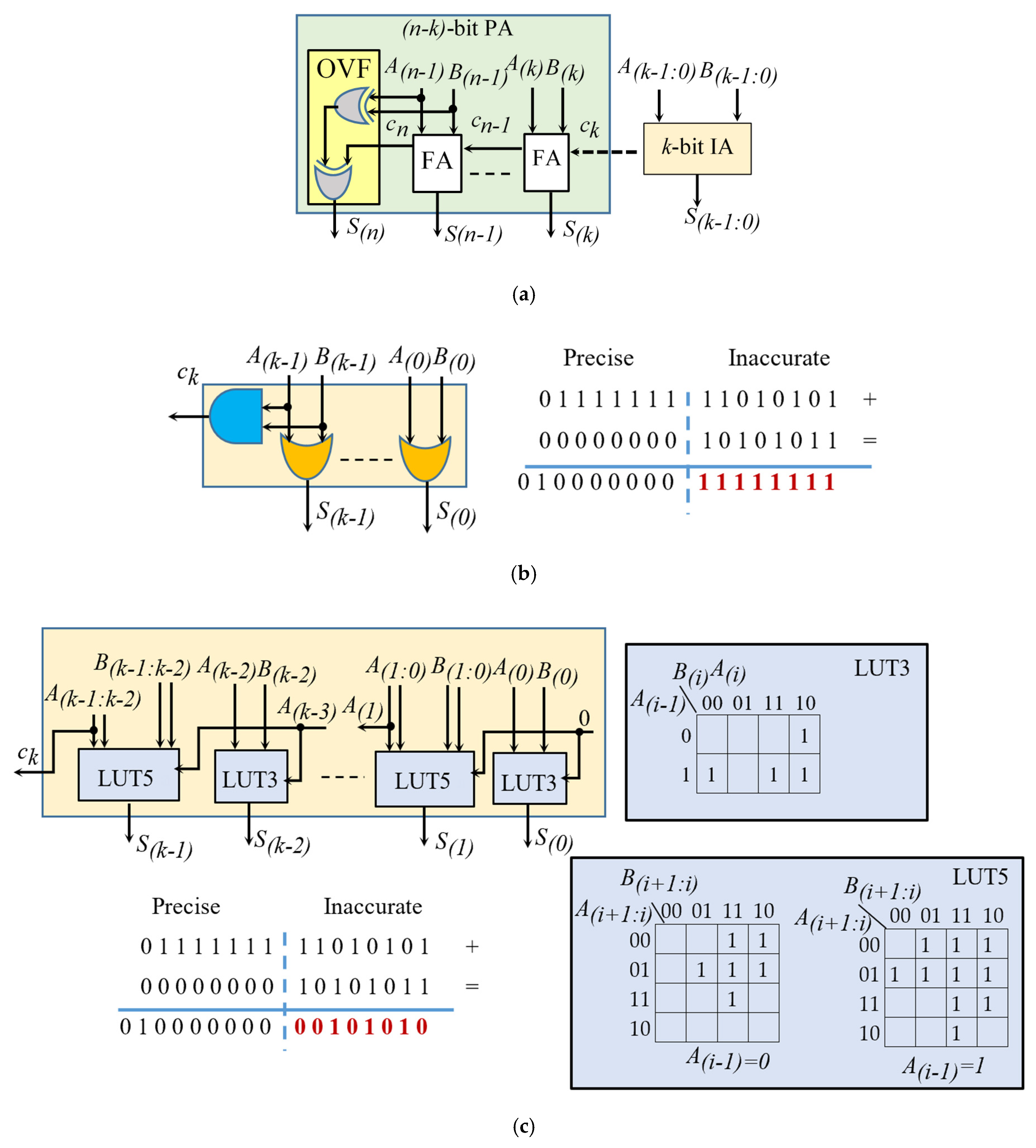
Figure 1a, while the
k-bit sub-words
ALSB and
BLSB are summed through an Inaccurate Adder (IA),
AMSB and
BMSB are inputted to a (
n −
k)-bit Precise Adder (PA). Having assumed to receive 2′s complement operands as inputs, the latter can perform its computation by exploiting (
n −
k) cascaded Full-Adders (FAs) and an auxiliary logic module to manage the eventual overflows (OVF). In some approximation schemes, the PA receives the carry-in signal
ck from the IA, whereas other approaches set
ck to a constant value. Anyway, the greater
k the higher the error introduced on the final (
n + 1)-bit result
S(
n:0).
When designed for the ASIC implementations, such an approximation strategy can be efficiently exploited by several addition structures, like the Ripple-Carry (RCA), the Carry-Look-Ahead (CLA), the Parallel-Prefix (PPA), and so on. Indeed, ASIC designs use the logic gates as the basic building blocks to achieve the desired circuit structure. Conversely, when the FPGAs are the target implementation platforms, the desired computational logic is generated using LUTs, DSPs, and dedicated interconnections. As it is widely known [
16,
17], the carry-propagate architecture makes the best use of the dedicated resources available within current FPGA devices for the implementation of fast carry chains [
19,
20]. For this reason, the approximate adders presented in [
13,
16,
17] and suitable for FPGA-based designs exploit the circuit topology schematized in
Figure 1a and they mainly differ from each other for the logic adopted within the sub-adder IA.
The example reported in
Figure 1b shows how two 16-bit signed operands are summed by the Lower-part OR Adder (LOA) presented in [
13], when
k = 8. As illustrated in the schematic and also depicted in
Figure 1b, the
k LSBs of the input data are just OR-ed to compute the sub-word
S(
k − 1:0). In this case, the carry signal
ck is also computed as the logic AND between the bits
A(
k − 1) and
B(
k − 1) to be then used in computing the sum bits
S(
n), …,
S(
k).
The design methodology presented in [
16] allows different topologies of approximate adders to be built in FPGA-based systems. There, the LUT primitives are directly instantiated by specifying their logic functions through the INIT attribute [
19]. Among the designs validated in [
16], the most accurate Approximate Adder-6 (AA6) is referenced in
Figure 1c. The INIT values used for the LUT3 and the LUT5 primitives employed in the sub-adder IA are ‘8E’ and ‘E080FEF8’, respectively [
16], which are equivalent to the Karnaugh maps also reported in
Figure 1c. The latter finally shows that, for the referred example of 16-bit addition, the result produced by such an approximate adder differs from that furnished by the LOA. Obviously, this is due to the different logic adopted by the IA sub-adder.
The Hardware Optimized and Error Reduced Approximate Adder (HOERAA) presented in [
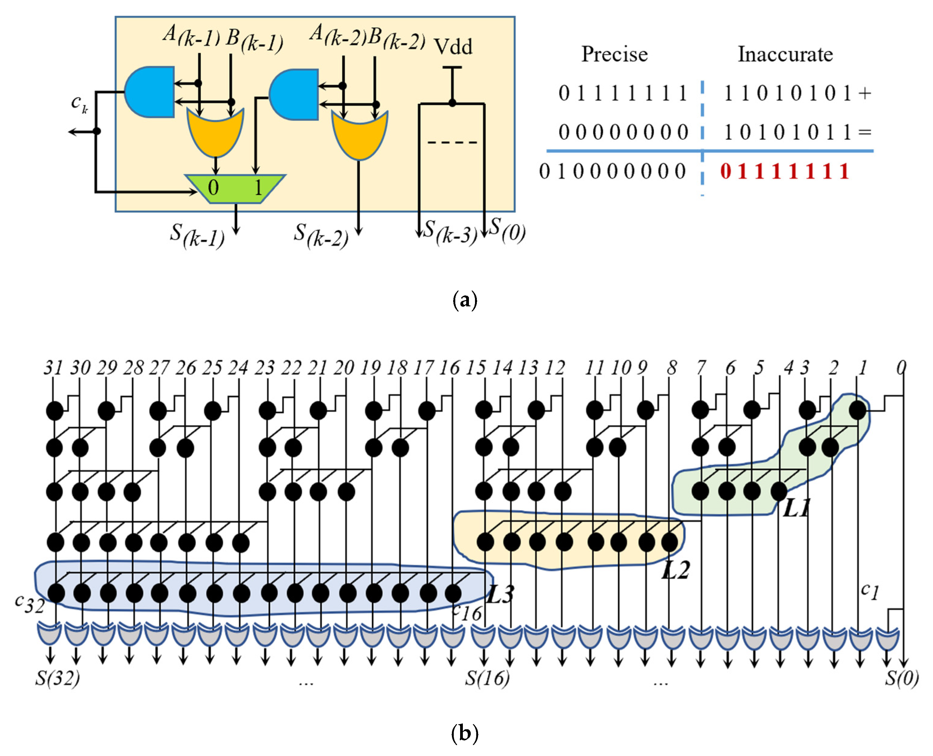
17] provides another different result. As depicted in
Figure 2a, such an adder sets the
k − 2 LSBs of the sum to a constant 1 (i.e., Vdd), whereas the two most significant sum bits of the sub-adder IA are computed by a simple multiplexing logic. It can be seen that, for the referred example, the result furnished by HOERAA differs from that generated by the LOA for the sum bit
S(
k − 1). Conversely, it differs from the sum produced by AA6 for all the even bit positions of the inaccurate portion of the output.
The embedded processor recently proposed in [
18] adopts a quite different strategy to design a 32-bit Approximate Sklansky Parallel-Prefix Adder. The latter computes, for each bit position
i of the operands, with
i = n − 1, …, 0, the propagate (
P(
i)
= A(
i) ⊕
B(
i)) and the generate (
G(
i)
= A(
i)·
B(
i)) signals that are then grouped through the classical DOT2 logic function to form the carry chains. As evident from
Figure 2b, five levels of DOT2 are necessary to furnish all the carry signals. The generic carry
cj, with
j = 31,
…, 1, is then XORed with the signal
P(
j) to produce the sum bit
S(
j). With the carry-in of the adder being assumed equal to zero, the least significant sum bit is equal to
P(0). Finally, the most significant sum bit is obtained by XORing the carry
c32 with the propagate signal
P(31), as required to manage the eventual overflows. As explained in [
18], three different levels of approximation can be achieved by omitting the DOT2 cells enclosed within the colored areas L1, L2, and L3 visible in
Figure 2b. Also, for this architecture, the most accurate condition is referred in the following. It occurs when only the DOTs within the L1 area are omitted.
3. The Novel Approximation Strategy
In line with most of the prior works described in the previous section, the approximation scheme here presented makes use of a k-bit IA and a (n − k)-bit PA, with k being the number of inaccurate LSBs introduced in the resulting sum. The main idea consists in splitting the k LSBs of the operands into 2-bit groups that are summed independently of each other. Obviously, many addition logics could be implemented to this aim. Anyway, in order to achieve the most accurate approximate results, the 2- and the 3-bit numbers closest to the correct 3-bit results obtained by summing 2-bit operands, with and without generating the carry-out signal, were examined.
The addition functions able to compute the most accurate 2- and 3-bit inexact attainable results are named ADD and ADDwc, respectively.
Table 1 compares these functions to the correct results produced when the generic 2-bit addition
A(
i + 1:
i)
+ B(
i + 1:
i) is performed with
ci being the incoming carry. It must be noted that both the approximate functions ADD and ADDwc assume the zero-incoming carry. Moreover, the former furnishes only the two sum bits
S(
i + 1) and
S(
i), whereas the latter generates the carry-out
ci + 2 as well. By implementing the approximations reported in
Table 1, the computational capability of the LUT primitives available within modern FPGAs can be efficiently exploited to perform the generic 2-bit addition taking the intermediate carry signal into account. Indeed, as it is well known, both Xilinx and Intel devices [
19,
20] provide fracturable LUTs that can support multiple logic functions. As an example, the generic LUT primitive can be configured to perform two 5-input logic functions. This means that the basic ADD function referred in
Table 1 requires only one LUT to provide the 2-bit sum
S(
i + 1:
i). Conversely, to furnish its three outputs
ci + 2,
S(
i + 1) and
S(
i), the function ADDwc must employ two LUTs.
Figure 3a illustrates the top-level architecture of the
k-bit inaccurate adder based on the proposed approach. It can be seen that the sub-adder IA employs
instances of the module ADD, each summing two adjacent bits of the operands
A and
B, and the module ADDwc, which computes the two most significant inaccurate sum bits,
S(
k − 1) and
S(
k − 2), and the carry signal
ck then inputted to the PA.
Figure 3a also reports an example of approximate addition performed by the proposed adder, whereas
Figure 3b,c illustrate, respectively, the gate-level structures of the modules ADD and ADDwc adopted here.
Several versions of the novel approximate adder have been implemented using the Artix-7 xc7a100tcsg324-3 device. In order to do this, parametric VHDL constructs were purposely written, and the Vivado Design Suite has been used to perform simulations, synthesis and implementations. Then, all the compared circuits were characterized in terms of resources requirements, computational delay, and energy consumption, assuming that, as typically happens in any digital data-path, inputs and outputs are registered. Preliminarily, post-layout validation tests were performed on 32-bit signed adders with
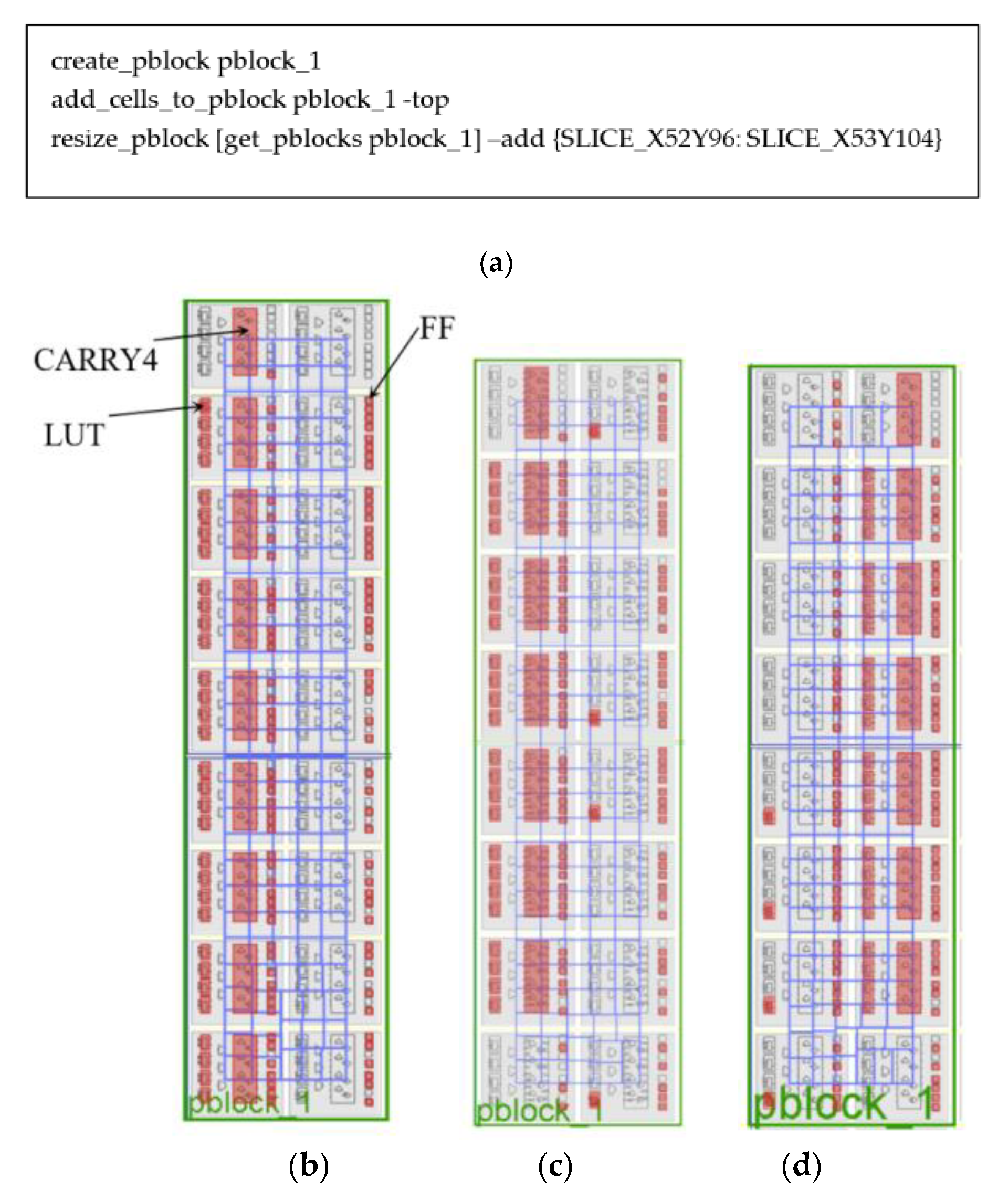
k = 2, …, 16. In order to avoid sparse and ineffective placements, the geometrical constraints reported in
Figure 4a have been adopted to implement all the characterized adders. Such constraints not only allow the employed LUTs, FFs, and 4-bit carry chains (CARRY4) resources to be mapped within a specific delimited rectangular area, but they ensure also that the clock distribution equally affects the energy consumption and the computational delay of all the implementations.
Figure 4b–d illustrate some of the laid out 32-bit designs, including the Full-Precision (FP) counterpart. It can be seen that the occupied resources (highlighted in red) are arranged in columns to fully exploit the dedicated carry-chain interconnections available on-chip [
19]. It is worth noting that the approximate adders New and AA6 [
16] of
Figure 4c,d span over carry chains shorter than the FP adder, thus using a reduced number of LUTs and CARRY4 primitives.
A sketch of the comparison results obtained for
k = 8 is reported in
Table 2. The latter includes the 32-bit FP Ripple-Carry Adder and the Sklansky Parallel-Prefix Adder presented in [
18] operating with the approximation level L1. It is worth highlighting that also the competitors were implemented by using the available LUTs as efficiently as possible. Post-placement, post-routing, and timing reports, automatically generated for each analyzed adder by the development tool, provided the number of used LUTs and FFs, as well as the minimum clock period. Moreover, the Vivado Report Power Tool has been used to estimate the power consumption of each adder based on the actual switching activity of the circuit internal nodes. The latter has been obtained by a post-implementation timing simulation by feeding the adder under analysis with 2000 couples of random input operands at its maximum clock frequency. It is worth noting that
Table 2 shows only the dynamic energy consumption of the adders: indeed, the static energy contribution depends only on the total number of hardware resources available on the chosen FPGA chip.
From
Table 2, it can be seen that, HOERAA excepted, all the compared architectures use the same number of Flip-Flops (FFs) to register inputs and outputs. Moreover, it must be noted that, as expected, the Sklansky adder is the most expensive in terms of occupied LUTs and the most energy hungry, whereas HOERAA is the cheapest and the less energy consuming architecture. This is due to its approximation strategy that, independently of the operands, always sets the
k LSBs of the output to 1, thus allowing both the resources and the energy dissipation required to compute them to be saved.
Table 2 also provides the parameters
L(
n,
k) and
F(
n,
k) that are the number of required LUTs and FFs, respectively, depending on the operands word-length
n and the number of inaccurate LSBs
k. Unfortunately, such a prediction is not as easy for the Sklansky adder.
In terms of the minimum clock period Tclk, it is interesting to note that while LOA [
13], HOERAA [
17], AA6 [
16], and the new adder, due to their approximate operating modes, are faster than the FP implementation, the Sklansky adder [
18] is ~67% slower. This is due to its inefficient way of using the dedicated resources available within the referred FPGA device for the implementation of fast carry chains.
Finally,
Table 2 reports the Average Error (AE), the Mean Error Distance (MED), and the Root Mean Square Error (RMSE) obtained by exhaustively simulating all the examined addition circuits. It can be seen that, in terms of MED and RMSE, the novel approximation scheme exhibits the best behavior. However, errors characteristics of the compared approximate adders are examined and discussed in more detail in the following sub-section.
In order to show how the hardware complexity of the novel approximate adder scales with
n and
k, post-layout characterization results obtained for
n = 64 and
k ranging from 8 to 32 are reported in
Table 3. As expected, the advantages achieved over the FP counterpart are even more evident: the energy consumption, the minimum clock period and the amount of occupied LUTs are reduced by up to 25%, 26%, and 14.4%, respectively.
Error Characteristics and Energy-Delay-Accuracy Tradeoff
As explained above, both the ADD and ADDwc modules employed in the novel approximate adder have been designed not only to reduce the number of cases in which an error is introduced on the performed additions, but also to drop the errors values, with respect to the competitors. In order to show that the approximation logic adopted here fulfills these features, let us analyze the errors introduced by the modules ADD and ADDwc in the cases above referenced in
Table 1 and summarized in
Table 4 and
Table 5, respectively. The errors introduced by the approximation schemes adopted in LOA [
13], AA6 [
16], and HOERAA [
17] are also reported to show that the proposed logic actually reduces both the number of cases in which an error is introduced and the errors values. It is worth noting that, for the adder AA6, two different conditions are referenced depending on the bits
A(
i − 1) and
A(
k − 3) that, as schematized in
Figure 1c, are used as the carry-in of the 2-bit additions performed to compute, respectively, the 2-bit sums
S(
i + 1:
i) and
S(
k − 1:
k − 2) [
16].
Table 5 also shows that, with respect to the correct results obtained with
ck − 2 = 0, only the approximation logic exploited here to process the most significant bit positions of the IA sub-adder does not introduce errors. Conversely, when
ck − 2 = 1, the ADDwc module introduces the constant error −1. As shown in the following, the behavior of the basic modules ADD and ADDwc allows the error characteristics of the
n-bit approximate adder designed as proposed here to be significantly improved with respect to the existing architectures.
In order to examine the accuracy behavior of the proposed approximation scheme, its errors distributions have been analyzed assuming the uniform distribution of two
n-bit signed operands
A and
B and considering values of
k ranging from 2 to 16. A similar analysis has been conducted for the competitors LOA [
13], AA6 [
16], and HOERAA [
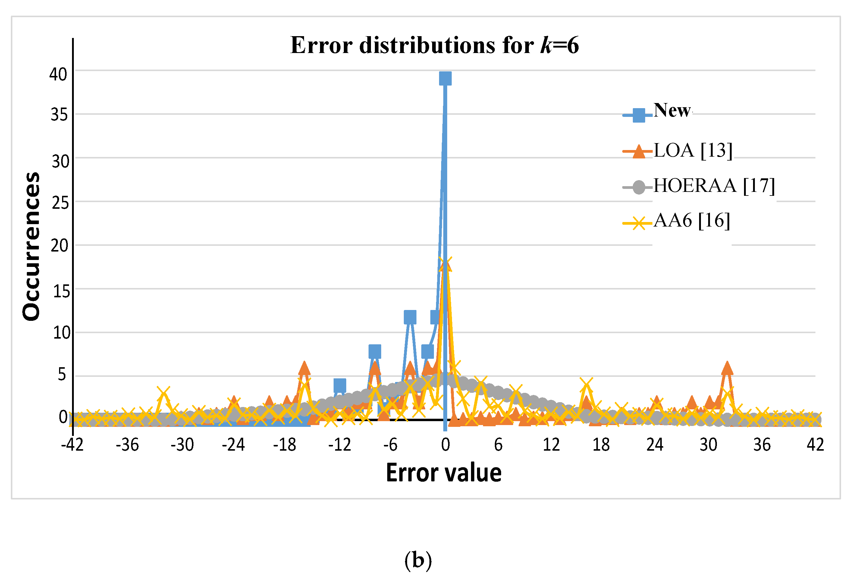
17]. Some of the obtained errors distributions are plotted in
Figure 5. The latter shows that, as expected, the novel approximate adder maximizes the occurrence of the zero error, and it does not introduce positive errors. This behavior has been observed in all the examined cases. Such an analysis has been useful also to evaluate the error ranges of the compared adders.
Table 6 clearly shows the better behavior of the novel adder over its counterparts in terms of both the minimum and the maximum errors even in comparison with the Sklansky adder presented in [
18].
Many error metrics have been evaluated through C++ software routines purpose-written to perform the exhaustive simulations for the cases in which
n-bit signed additions are executed with
k ranging from 2 to 16.
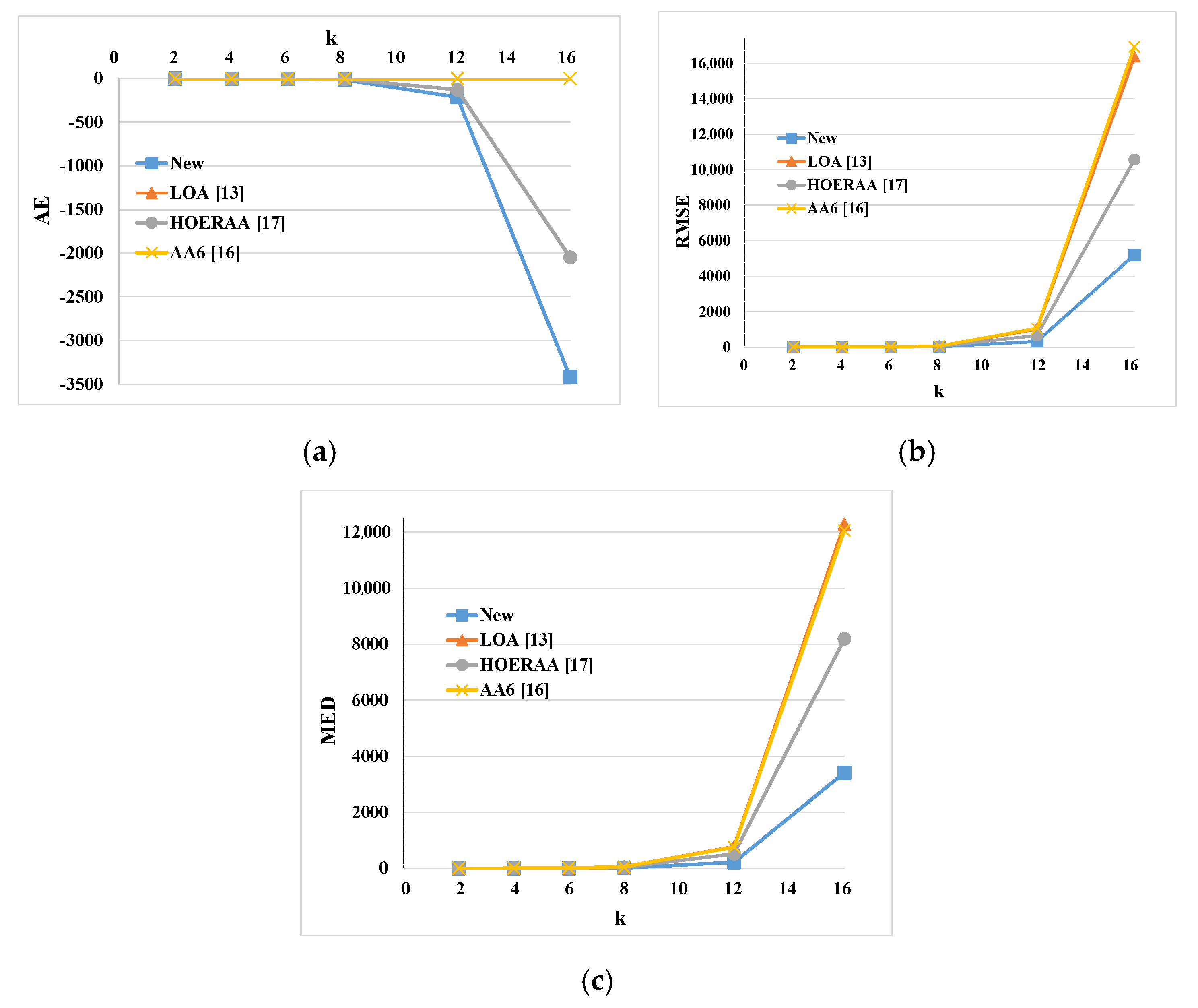
Figure 6 plots the AE, the MED, and the RMSE obtained, as defined in [
6], for all the compared approximate adders.
As visible in
Figure 6a, the approximation schemes LOA [
13] and AA6 [
16] keep their AE constant, respectively, to 0.25 and 0, independently of
k. Conversely, the AEs related to HOERAA [
17] and to the proposed adder decrease as the value of
k increases and the new approximate adder seems to perform worse than its counterparts. Anyway, it must be noted that in contrast to its competitors, the proposed adder does not introduce positive errors that compensate for the negative ones, with the obvious effect on the AE. Moreover, as deeply discussed in [
6], the RMSE and the MED are more effective error metrics to establish which approximate adder introduces lower errors. Results plotted in
Figure 6b,c demonstrate the much better behavior of the new approximation scheme that, at a parity of
k, exhibits RMSE values ~49% lower than HOERAA and ~70% better than LOA and AA6. Even better results are obtained in terms of MED, which is reduced by ~58% with respect to HOERAA and by ~72% with respect to LOA and AA6.
The new approximate adder has also been compared to its counterparts in terms of energy-delay-accuracy tradeoff. In order to do this, the energy-delay product (EDP) was evaluated versus the MED and RMSE error metrics. The design spaces reported in
Figure 7 clearly demonstrate that a 32-bit adder designed as proposed here exhibits the best EDP-accuracy tradeoff in all the examined cases. Indeed, at a given
k, it can achieve accuracy values that cannot be reached by any other competitor. Moreover, the novel approximate adder configured for
k = 2 does not introduce any error and exhibits an EDP ~4% lower than the FP counterpart. In comparison with AA6 at any given
k, the new adder, thanks to its less complex combinatorial logic and the lower number of interconnections, also offers a better EDP. Conversely, when
k ≤ 8, the adders HOERAA and LOA reach slightly lower EDPs, due to their simplified strategies adopted to approximate the
k LSBs, which clearly affect both the MED and the RMSE. As expected, this effect is more evident in HOERAA for higher
k values. However, it is worth noting that when
k ≥ 12 the approximation strategy adopted in HOERAA achieves a ~17% lower EDP, but with the MED and the RMSE almost doubled with respect to the novel scheme.
4. The 2D Digital Image Filtering as a Case Study
To ascertain how the novel approximate adder affects the accuracy of more complex computations, it has been applied to approximate the 2D digital image filtering. The latter processes an H × W input digital image by convolving each x-bit pixel IP(h,w) of the image, with h = 0, …, H − 1 and w = 0, …, W − 1, by the chosen g × g filter. In order to do this, a g × g neighborhood is windowed around IP(h,w). Then, the pixels and the coefficients located at the homologous positions in the neighborhood and in the filter are multiplied by each other. To compute the multiplication between the generic x-bit pixel IP and its homologous y-bit coefficient C, y partial products PPj (with j = 0, …, y − 1) are computed, one for each bit of the multiplier C. They are then aligned with each other, by left shifting each PPj by j bit positions; and finally, the partial products are summed to generate the (x + y)-bit result.
Among the various possible choices to introduce the approximate addition in the computation of the generic multiplication, as depicted in
Figure 8a, the solution chosen in the case study adds the partial products through
y − 1 cascaded approximate adders. In particular, for each
PPj, with
j > 1, an approximate addition is performed with
j + 1 inaccurate LSBs to take into account that, due the aligning left shifts,
PPj has
j LSBs equal to zero. The
g × g approximate products
PRp (with
p ranging between 0 and
g × g − 1) obtained in this way are then accumulated through an adder tree structure that, as illustrated in
Figure 8b, consists of
levels of two operands additions, all performed by introducing
k inaccurate LSBs. The accumulation furnishes the
-bit filtered pixel
OP(
h,w).
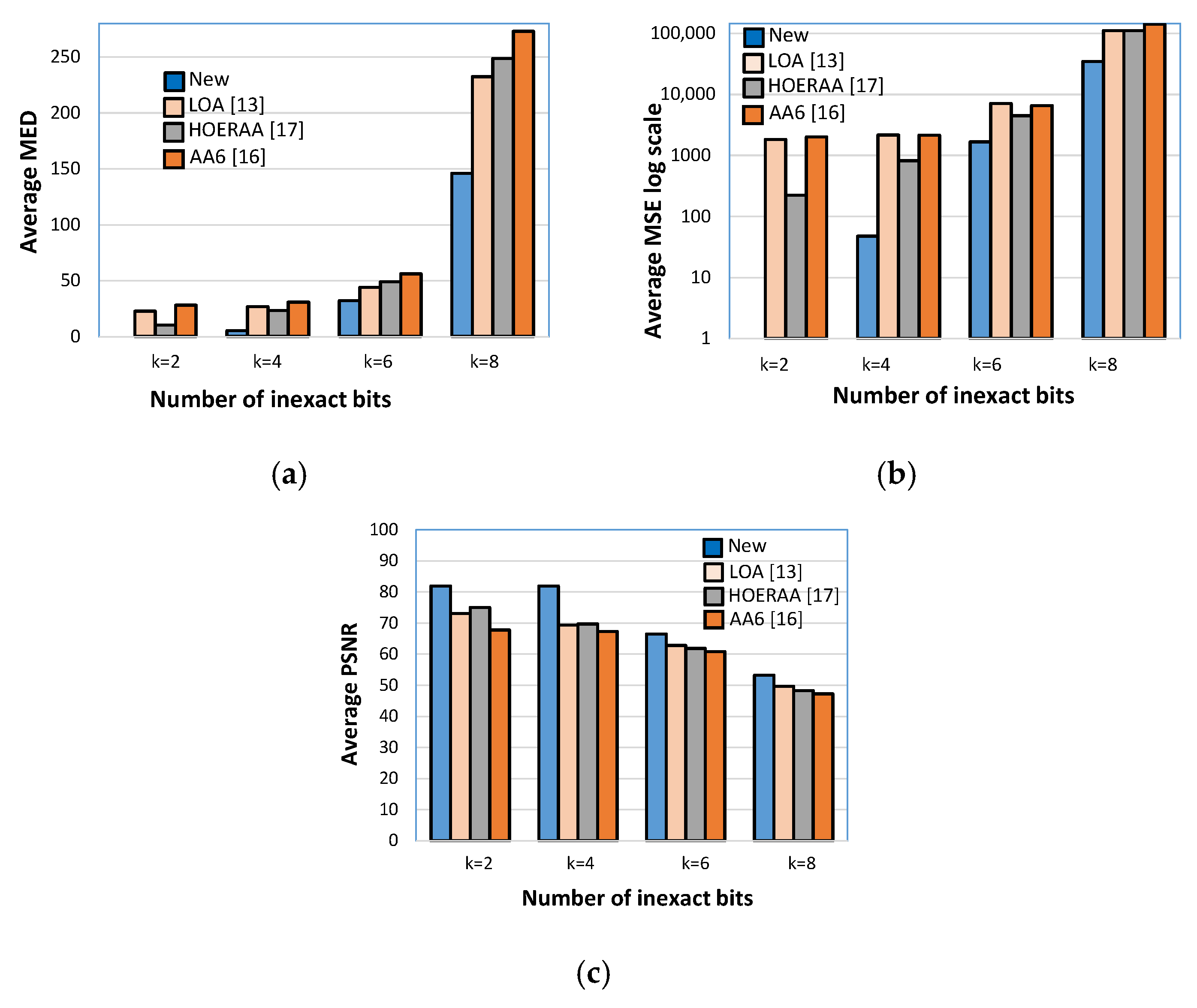
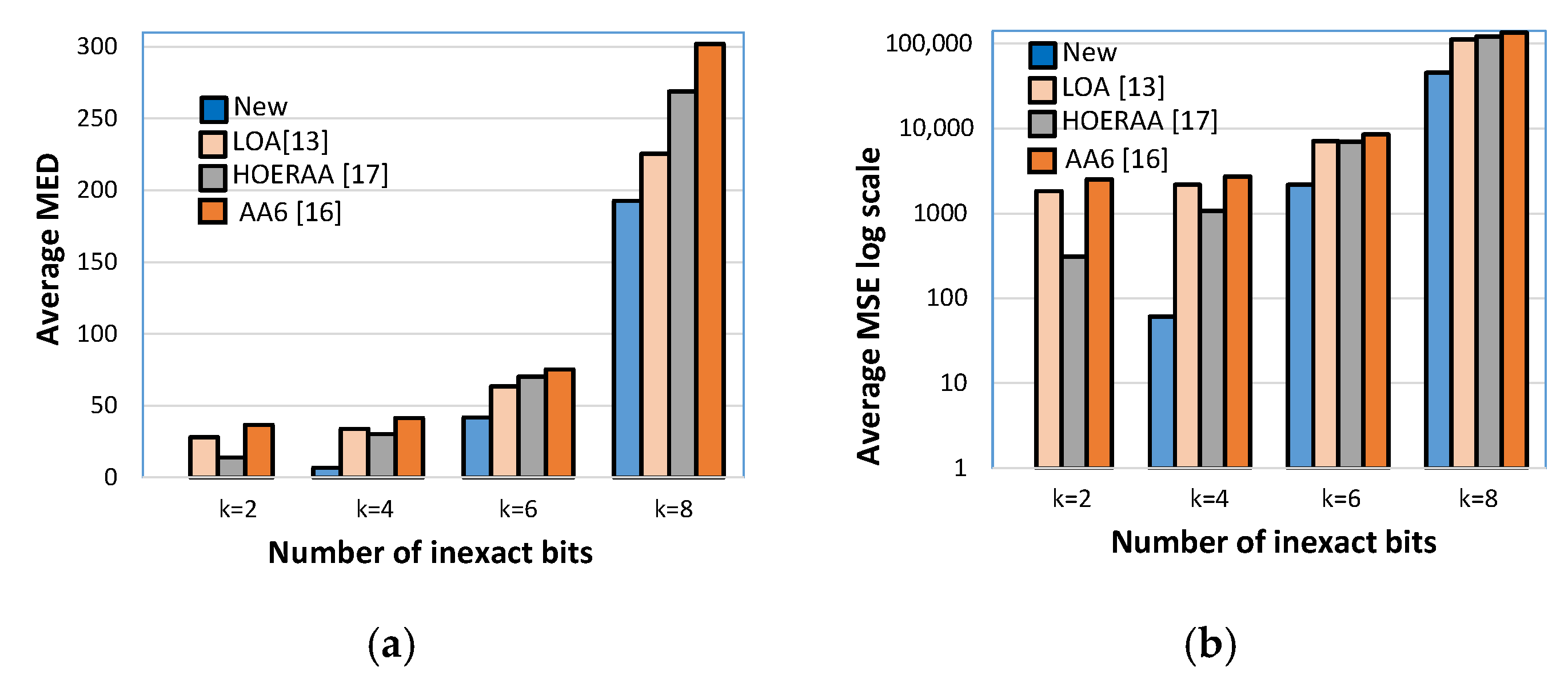
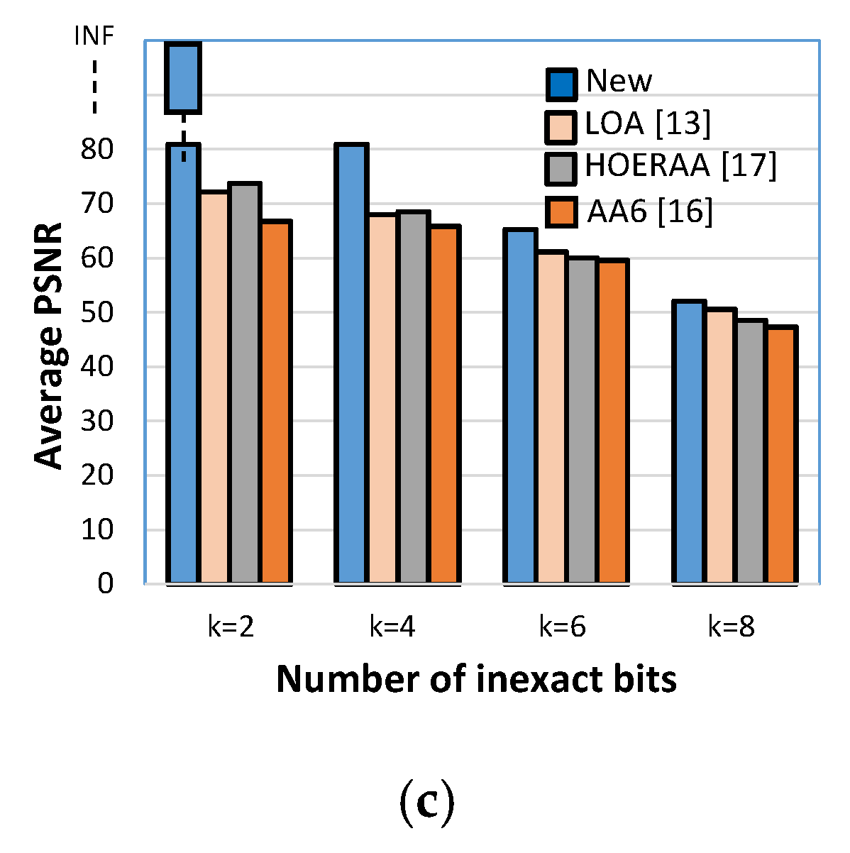
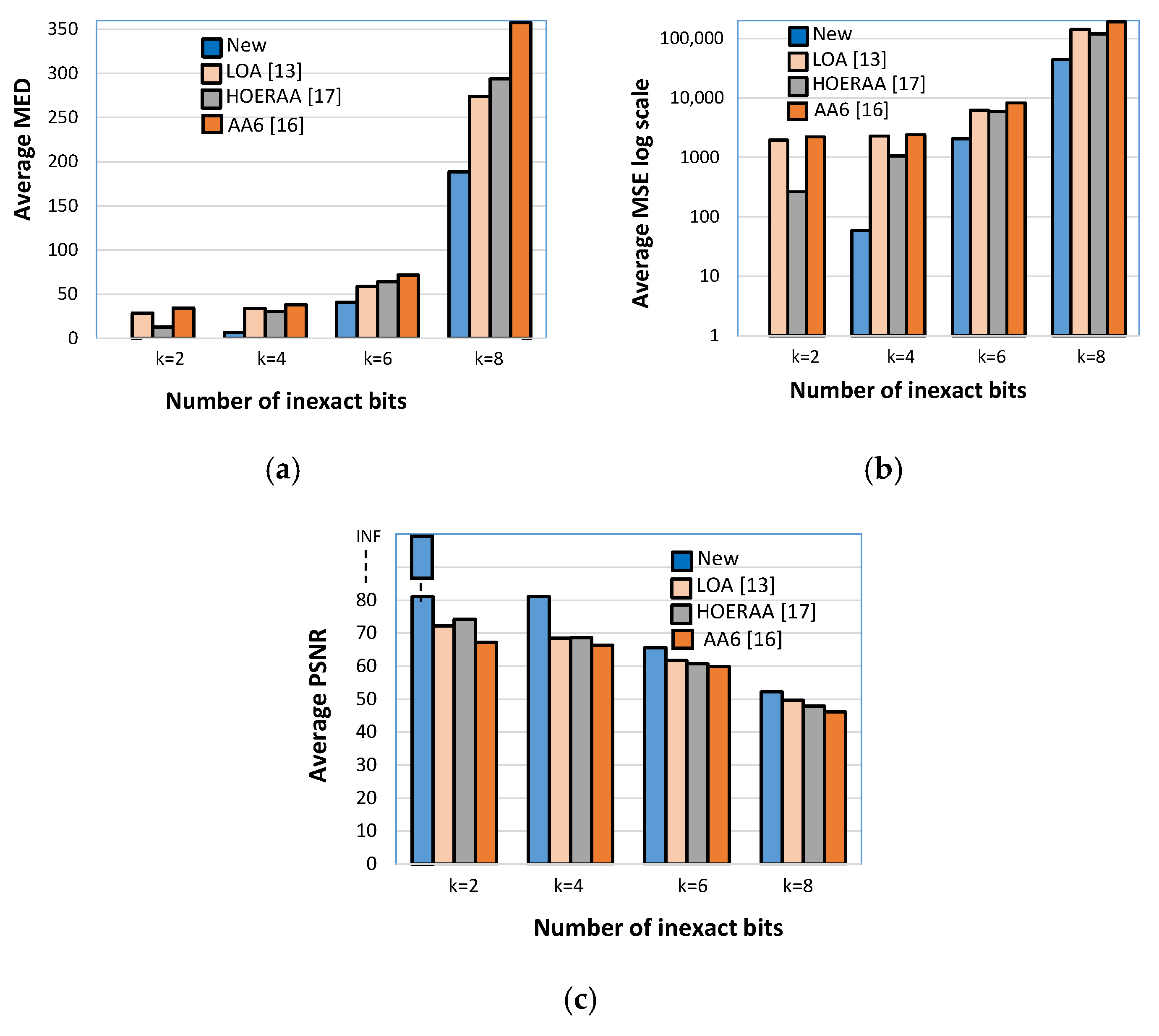
The accuracy achieved by the above described approximate filtering when the 256 × 256 pixels greyscale benchmark images Lena, Cameraman, and Peppers are filtered using the 3 × 3 Laplacian, Gaussian Blur, and Sobel kernels has been deeply evaluated. The MED, the Mean Squared Error (MSE), and the Peak Signal-to-Noise Ratio (PSNR) have been measured with
k varying from 2 to 8. For the purposes of comparison, the effects introduced in the same operating conditions by the approximate adders LOA [
13], HOERAA [
17], and AA6 [
16] have also been evaluated. The results obtained for each testbench image in terms of MED, MSE, and PSNR, and averaged over the used filters, are plotted in
Figure 9,
Figure 10 and
Figure 11.
The latter demonstrate that, independently of the processed image, the approximate filter based on the inaccurate addition here proposed always minimizes both the MED and the MSE and ensures the highest PSNR to be reached. As an example, referring to the Lena benchmark image, with k = 6, the new approximation scheme leads to an average MED 80%, 77%, and 82% lower than those obtained with the LOA, HOERAA, and AA6 approximation logics, respectively. Moreover, it allows an average MSE ~39×, ~17× and ~2000× lower to be achieved over the competitors, with an average PSNR improved by ~17%, ~18% and ~22%.
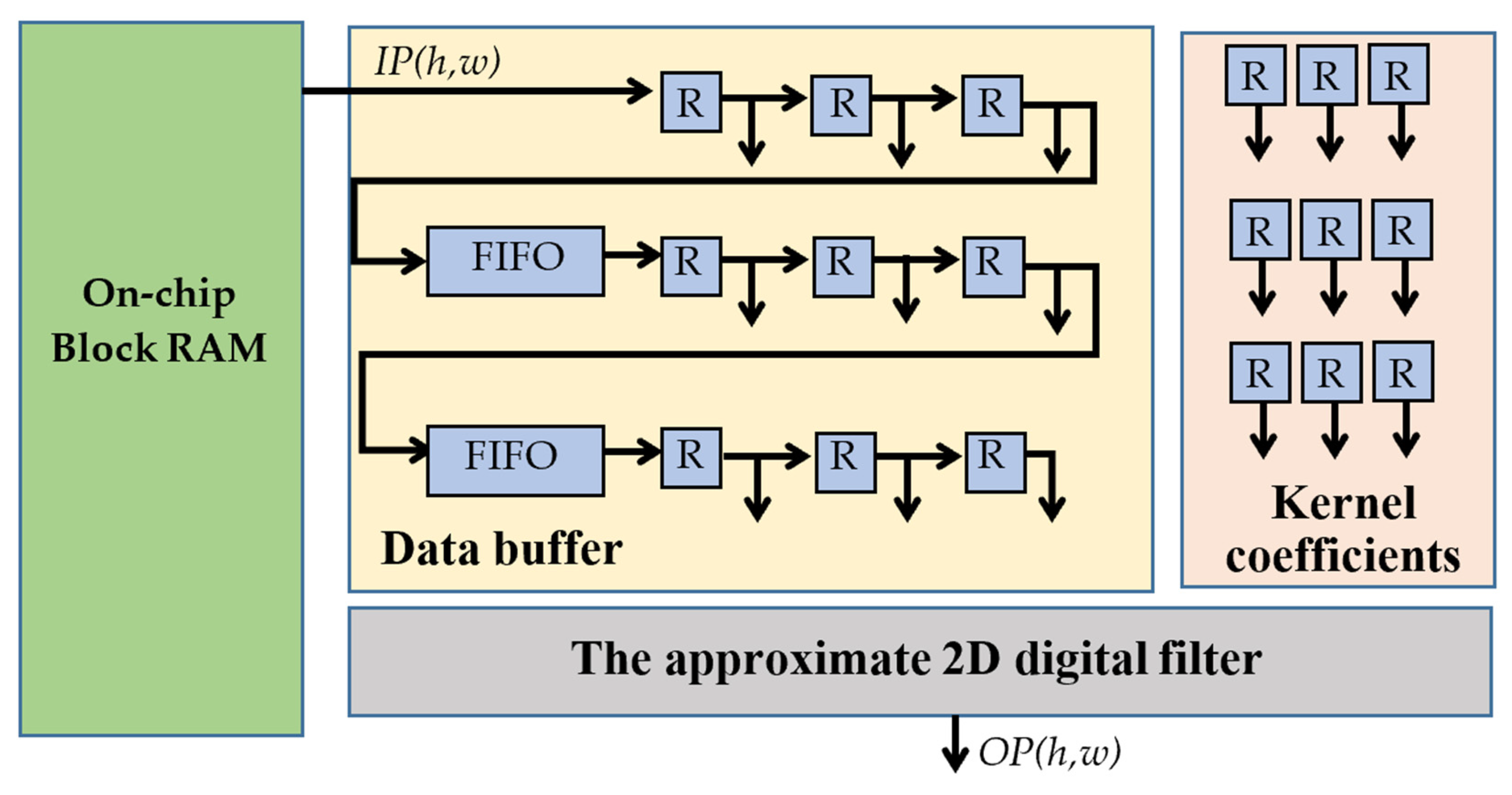
The VHDL description of the approximate 2D digital filter architecture above analyzed in terms of accuracy has also been implemented and characterized in terms of energy consumption, computational delay, and resource requirements. To this aim, the 3 × 3 Laplacian filtering on 256 × 256 greyscale images has been chosen as a case study. As illustrated in
Figure 12, the input pixels are stored within an on-chip auxiliary memory block. Then, they are transferred to an appropriate data buffer. The latter exploits two 253 depth First In First Out (FIFO) local memories and 3 × 3 8-bit registers (R) to accommodate the 3 × 3 windows of pixels that are then sent to the approximate 2D digital filter, which receives also the kernel coefficients stored in dedicated registers. The approximate 2D digital filter uses nine multipliers and an adder tree structured as above shown in
Figure 8a,b, respectively. For the generic window of pixels centered at
IP(
h,w), the approximate filter computes the required nine products and accumulates them, thus furnishing the filtered pixel
OP(
h,w).
Table 7 summarizes the post-implementation results obtained for several values of
k adopted in the adder tree of
Figure 8b. The FP counterpart implementation is also reported as a reference. It can be seen that the adopted approximation strategy allows the dynamic energy dissipation due to the clock distribution (Eclk), the switching activity of the internal signals (Esignals), and the used logic resources (Elogic) to be reduced by up to ~15.4%, ~35%, and ~29.9%, respectively. Obviously, the energy contribution due to the BRAM accesses (EBRAM) does not benefit from the approximate technique. However, an overall energy consumption (Etot) up to 18.7% lower than the FP counterpart is achieved.
To evaluate the drawbacks of the novel approach, a further analysis is reported in
Figure 13, showing the quality gain attainable with respect to the competitors versus the energy penalty. For the sake of conciseness, plots show average results obtained for the filters implementations referring to the above-mentioned image benchmarks. More in detail, the points labelled as New-LOA, New-HOERAA, and New-AA6 plot the quality gained by the 2D filter based on the new approximation strategy over those based on the approximate adders LOA [
13], HOERAA [
17], and AA6 [
16] versus the penalty paid in terms of energy. These results show that the quality improvement, in terms of MED (
Figure 13a), MSE (
Figure 13b), and PSNR (
Figure 13c), achieved by exploiting the new approximate adders at a parity of
k, is obtained at an expense of an additional energy quota that is several times smaller, and in most cases one order of magnitude lower than the advantage in terms of computational precision.
5. Conclusions
This research work has presented a novel approximation technique to design fast and low-power adders suitable for FPGA devices. The proposed strategy efficiently exploits the configurable resources available within FPGAs to significantly improve the quality over the state-of-the-art approximate adders, while exhibiting similar computational delays and energy consumptions. In particular, the approximate adder presented here computes each couple of consecutive sum bits by taking into account the internal intermediate carry signal, which is properly generated to correct both the bit positions, thus minimizing the error introduced on the generic 2-bit addition.
For the purposes of comparison with state-of-the-art competitors, several implementations of the novel approximate adder have been characterized in terms of resources requirements, energy consumption, computational delay, and standard error metrics. For the 32-bit configuration, varying the number of inaccurate LSBs k from 2 to 16, the proposed design always demonstrates the best EDP-accuracy tradeoff.
Finally, the 2D digital image filtering has been chosen as a case study to compare the performances offered by the novel approximation technique with the ones obtained by the competitors in more complex elaborations. The proposed approximate adder has shown its superiority in all the examined conditions, presenting, at a parity of k, a quality improvement several times greater, and in most cases, one order of magnitude higher, than the energy penalty.
