Review

A Review on Evaluation and Configuration of Fault Injection Attack Instruments to Design Attack Resistant MCU-Based IoT Applications

1
LCIS Laboratory, University of Grenoble Alpes, Grenoble INP, 26000 Valence, France
2
Department of Computer Engineering, Bogazici University, 34470 Istanbul, Turkey
*
Author to whom correspondence should be addressed.
Electronics 2020, 9(7), 1153; https://doi.org/10.3390/electronics9071153
Submission received: 31 May 2020 / Revised: 7 July 2020 / Accepted: 11 July 2020 / Published: 16 July 2020
(This article belongs to the Section Computer Science & Engineering)

Abstract

:
The Internet-of-Things (IoT) has gained significant importance in all aspects of daily life, and there are many areas of application for it. Despite the rate of expansion and the development of infrastructure, such systems also bring new concerns and challenges. Security and privacy are at the top of the list and must be carefully considered by designers and manufacturers. Not only do the devices need to be protected against software and network-based attacks, but proper attention must also be paid to recently emerging hardware-based attacks. However, low-cost unit software developers are not always sufficiently aware of existing vulnerabilities due to these kinds of attacks. To tackle the issue, various platforms are proposed to enable rapid and easy evaluation against physical attacks. Fault attacks are the noticeable type of physical attacks, in which the normal and secure behavior of the targeted devices is liable to be jeopardized. Indeed, such attacks can cause serious malfunctions in the underlying applications. Various studies have been conducted in other research works related to the different aspects of fault injection. Two of the primary means of fault attacks are clock and voltage fault injection. These attacks can be performed with a moderate level of knowledge, utilizing low-cost facilities to target IoT systems. In this paper, we explore the main parameters of the clock and voltage fault generators. This can help hardware security specialists to develop an open-source platform and to evaluate their design against such attacks. The principal concepts of both methods are studied for this purpose. Thereafter, we conclude our paper with the need for such an evaluation platform in the design and production cycle of embedded systems and IoT devices.

1. Introduction

In recent years, the Internet of Things (IoT) concept has enabled embedded systems to communicate via internet protocols to coordinate decisions [1]. IoT can provide smart services for end-users and eases the use of distributed systems. The broad adoption of IoT-enabled embedded devices highlights the need for safe functionality as well as data security and confidentiality, specifically when they are employed in safety-critical applications [1,2,3]. Typically, the main target of adversaries is to discover ‘Achilles’ heels’ in the system so as to make effective attacks against the application running on the processing unit. This can lead to a breakdown of the system’s normal functionality, disruption of the execution of program flow, and the gaining of unauthorized access or leakage of highly secured information. Therefore, manufacturers or designers should adopt a set of guidelines to ensure the secure development and deployment of these devices while striving to provide a large variety of efficient and free services to the users.
Many network or software-based vulnerabilities have been discussed in the literature [4]. Subsequently, numerous countermeasures are proposed and employed to secure the systems against the mentioned vulnerabilities [3,5,6]. However, with the advent of hardware-based attacks in the recent decade, achieving a high level of security has become more challenging, and attackers can easily subvert many types of protections and encryptions [7,8,9,10,11]. Therefore, protecting firmware and data within IoT devices against these attacks is of decisive importance. This issue becomes even more important when the adversaries target safety-critical embedded systems to exploit various vulnerabilities efficiently and pose significant risks by performing these attacks [12]. Nevertheless, time-to-market and IoT production costs take priority over prudent security practices, and in most cases, hardware-based vulnerabilities have not yet been well explored by the embedded software developers [13]. To systematically address this issue in IoT system design, there must be different evaluation stages which cover hardware-based threats as well as software and network ones.
A hardware security assessment can be performed either by applying practical techniques, including simulations and experimental techniques, or by using mathematical analysis methods [12,14,15,16]. Today’s simulation tools have extensive capabilities, and they can be used as highly accurate, flexible, and low-cost appliances in primary evaluation. However, in the domain of hardware-based attacks, since different environmental parameters are involved, it is not possible to describe and study any arbitrary attack in the simulation environment [17]. Moreover, using hardware simulators and accessing the processor hardware description is not feasible for the software developers. Another approach of security assessment is by mathematical analysis, which is also essential for primary appraisal steps [15]. Nevertheless, this technique cannot guarantee a high-quality assessment against hardware-based attacks that target post-implemented devices [14]. Technical considerations—including environmental effects, process variations, and subversive influences—still have a place [17]. The most considered technique for hardware security evaluation is based on experimental analysis that can provide a physical environment for investigating and measuring the consequences of possible risks [18,19,20]. To this end, an easy to use and practical evaluation platform for the embedded-software developer is a fundamental requirement in order to emulate, monitor, manage, and analyze vulnerabilities in the code.
In the hardware security domain, one of the most prominent and powerful tools in the hands of adversaries is physical attack [21,22]. Physical attacks are the type of attack in which the attacker has access to the targeted device. These attacks can help the adversary to intrude into the IoT [7,9,12]. Physical attacks are divided into two categories, namely, passive and active attacks [12,23]. In passive attacks, the targeted device behaves normally, and the attacker’s main goal is not to leave any trace or manipulate the target’s regular functioning [24]. In point of fact, such attacks are based on correlating the system activity with an observable physical parameter such as power consumption, execution time, or electromagnetic emission. Correlation power analysis against cryptographic operation is a well-known example that allows cryptographic key identification by physical measurement [25,26]. As the second category, active attacks are a type of attack in which the adversary actively tampers the target device by stressing its available input channels. Moreover, variations in environmental parameters, such as temperature, can also be used to induce faulty behaviors and cause disruptions [10]. One of the well-known types of active attacks widely studied during the last two decades is fault injection attack (FIA). FIAs are usually accomplished by manipulating either environmental parameters or inputs [27,28,29]. FIA has been demonstrated to be a powerful technique to reveal secret data with a small number of experiments [12,30]. Through FIAs, intruders can accomplish several objectives. Among these objectives, the two principal ones are: (1) To cause erroneous outputs and to disturb the normal behavior through bypassing specific operations on some occasions [7,8,27]; and (2) to extract secret information by using faulty outputs [30,31].
Fault injection attacks can be further classified into three different categories, namely, invasive, non-invasive, and semi-invasive [28]. Invasive attacks are the type of intrusions performed by de-packaging the integrated circuit (IC) and modifying the physical properties to do some probing. Invasive attacks—such as micro-probing, laser, or optical fault injection—are the strongest physical attacks without imposing any restrictions on accessing the inside of the chips [21]. These kinds of attacks are very powerful in precise space-time positioning, and they can reveal considerable secret information from internal parts of the chip to the attackers. However, they are expensive, mostly irreversible, and complicated. In addition, they have to be performed by qualified specialists in laboratories equipped with special devices. They are usually applied against very secure devices such as smartcards or complex commercial off-the-shelves (COTS) components, in which the target is in the form of industrial products, and the attacker usually has more features and knowledge [32]. Nonetheless, they are not proper methods for individual IoT hackers because they are too costly for them, and also they do not have access to wide-range facilities. Non-invasive attacks are the type of non-destructive attacks that can be accomplished by only utilizing pin-probing or bus-snooping without damaging the package [21]. Two of the simplest non-invasive fault attacks are tampering the device clock signal and/or the supply voltage, the so-called clock and voltage glitch attacks [12]. In particular, non-invasive attacks are more threatening than invasive attacks for IoT devices. This is for three main reasons: (1) since this kind of attack does not require any physical tampering, the owner of the targeted device might not notice the attack and trust in functionality and information security. (2) They can be reproduced and updated using low-cost and existing types of equipment, even in a small laboratory [25,33]. (3) They have proven that a high success rate can be achieved in a short time [11]. The semi-invasive attack is a type of FIA that stands between invasive and non-invasive attacks [34]. This type of attack can involve de-packaging the IC layers to gain access to the internal surface of the target, but normally, the passivation layer remains unimpaired. For instance, optical fault injection is a semi-invasive attack, in which the protection layer of the device has to be ruined [34]. In this paper, we focus on the voltage and clock glitches because they do not need package modification, they are low cost, and precise in producing the intended results. Moreover, they are the most used techniques in attacks against IoT devices with medium security.
Security evaluation against fault attacks is a key step in the design of any IoT device that needs to adhere to specific security requirements [16,35]. To this end, hardware security specialists should design an efficient evaluation platform for the embedded software developers of critical IoTs. These developers need to employ and use these platforms to investigate existing vulnerabilities. Usually, the experimental-based evaluation platforms for FIAs mimic the real fault attacks. Currently, there is a large and complicated realm of known fault attacks in the literature, which makes it difficult for a hardware security engineer to provide software designers with an applicable and accurate evaluation platform to test their products against attacks. Reference [36] surveys some of the fault injection techniques on cryptographic applications including differential fault analysis (DFA), collision fault analysis (CFA), and ineffective fault analysis (IFA). Then, it provides countermeasures which can somehow mitigate the impacts of the fault injection attack. Reference [16] reviews and compares the features of various fault injection approaches in digital circuits. They focus on three main type of software-based, emulation-based, and hardware-based fault injection approaches. Then, they explore the requirements for advanced hardware based attacks. Reference [22] studies the hardware-based fault attacks on software with emphasize on the scope of embedded systems. It discusses the main techniques for fault injection attack and the behavior of the system in front of them. Then it analyzes the fault propagation through the architecture and the embedded software. None of previous survey papers have a detailed focus on having a low-cost and easy to implement clock and voltage fault injection instrument. Therefore, in this work, we comprehensively review the most important instruments for clock and voltage glitches. This paper reviews different existing security evaluation platforms and compares their main characteristics. This can specifically help those who attempt to design an evaluation platform that covers the most recent required features and characteristics of fault injection methods. It should also be noted that these features are highly dependent on the attacker’s target. For this purpose, in this paper, we first determine the main features of each fault injection method and then study and compare the related works for each approach. Finally, we define the related characteristics of an efficient fault injection evaluation platform, according to the studied works. This can help hardware security engineers to better understand the main features of a fault injection evaluation platform and to improve practical fault injectors to be used by software developers. In conclusion, this paper aims to highlight the best-presented ideas for clock and voltage fault attack evaluation configurations and designs. Comparing these ideas and platforms, we can define the properties of a framework, which security engineers need to develop or customize based on their applications.
This paper is organized as follows: Section 2 describes the basic concepts regarding clock and voltage glitching fault attacks and defines all the main parameters related to the fault injectors. Section 3 and Section 4 review the state of the art of clock and voltage fault injectors and compare them by using different metrics. Section 5 outlines the characteristics of an efficient evaluation platform for IoT devices. Finally, Section 6 presents the conclusion of this work.

2. Preliminaries and Basic Concepts

Accurate design of a comprehensive hardware-based security assessment tool that can be used by software developers calls for extraction of the attack attributes, i.e., clock and voltage glitch; characteristics; and requirements. In this paper, we assume that secure embedded software developers consider that the underlying hardware has no vulnerabilities. In other words, they assume that designing secure software is sufficient to guarantee the security of the entire system, and they do not consider hardware-level malfunction risks. Below, we first present the basic set-up for the fault injection attack. Obviously, the fault generator is the most important part of a fault injection system. Therefore, in this paper, we elaborate first on the main characteristics of the generator, which affect the success rate of the attacks. In order to generate operative faults in the system, the generator must be able to produce effective manipulations that can intrude into the systems. For this reason, we review the basic implications of why and how changes in the clock and voltage inputs lead to errors in the target system. The attack scenarios may have different characteristics based on the considered vulnerabilities in the application running on the target system. When the necessary characteristics are covered, successful attacks can be implemented even at low cost and with moderate knowledge.
Among various types of physical attacks, we have focused on fault injection as one of the most important types of semi-invasive attacks. Figure 1 shows the experimental set-up for the fault injection system. It includes a target board (device under test), a fault generator, and a controller computer. Generally, in the hardware-controlled fault injection techniques, a separate external fault generator is used to perform the physical attack on the target and to induce faults in the running application. It is essential that the attacker produces well-controlled faults in the generator in order to achieve the desired results. It is, therefore, a challenging procedure to develop a fault generator with a high level of accuracy and precision. Several factors determine the applicability and efficiency of a fault generator. These factors for the clock and voltage fault attacks include accuracy, development expenses, complexity of the system set-up, and user expertise.
Below, we identify a list of features regarded in the literature as being the main ones for a hardware-based fault generator [11,19,27,29,37,38,39,40,41]:
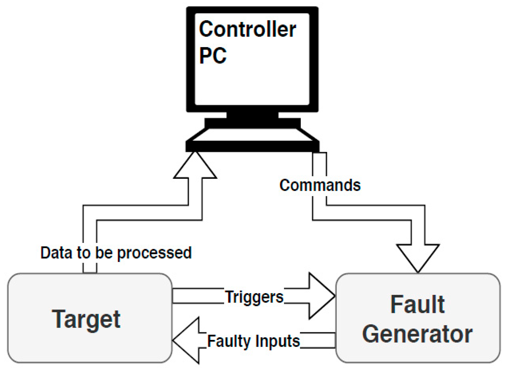
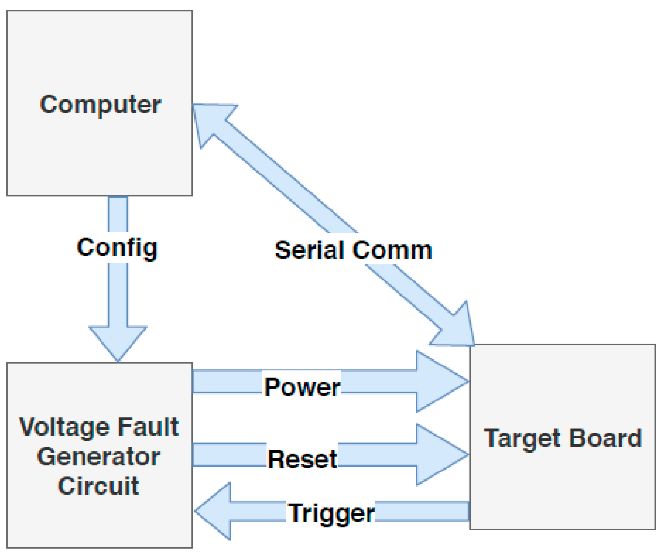
  • Accuracy in the generated faulty signal: This parameter is described according to the type of the signal produced. In fact, the more control we have over the generated faulty signals, the more we achieve successful attacks in terms of generating and exploiting the desired faults. Control over the time and location of injected faults can be achieved using the communication lines between the controller PC and the fault generator.
  • Run-time fault configuration: In some evaluation platforms, the parameters of a faulty signal produced by the generator can be reconfigured during run-time. They are not limited to the design time and can be used to test a target system during the attack phase. This feature is available in some generators and is based on some kinds of FPGAs, allowing modification of some parameters during the run time [19].
  • Reproducibility of the faulty signal: Reproducibility is the ability to obtain the same results in multiple repeats of the same test. Regarding this feature, the faulty signal should be reproducible and validated by a third party if the same hardware is used (for example, the same FPGA). This parameter becomes more important when a unique evaluation platform is designed and used for faulty signal generation [11,19,27,29,37,40,41].
  • Randomness in faulty signal: Many of the faulty signal-generating methods presented, such as [7,9,10,18,19,27,28,37], are deterministic methods. To set up a fault generator and to apply an attack with high accuracy, all the output parameters must be prepared and calculated. However, as this requires complete and adequate information about the target, it is not applicable in all real-world attack scenarios. In addition, in order to achieve an efficient attack, a large number of possible combinations of the fault injection parameters need to be covered. This makes deterministic methods intractable within a limited time. To address this issue, a fuzzy-based fault generator has been proposed. It has been reported that this method has a high attack success rate [38]. In Section 3, we elaborate further on the related works.
In the sub-sections below, we review the basic concepts and significant parameters in clock and voltage fault injection methods.

2.1. Clock-Based Fault Attacks

Clock-based fault injection is a low-cost attack that can be applied by the attacker to devices supplied with an external clock such as smart cards. If the target uses an internal clock signal, this method is often not applicable. The fundamental concepts and related characteristics for this approach are provided in this sub-section.

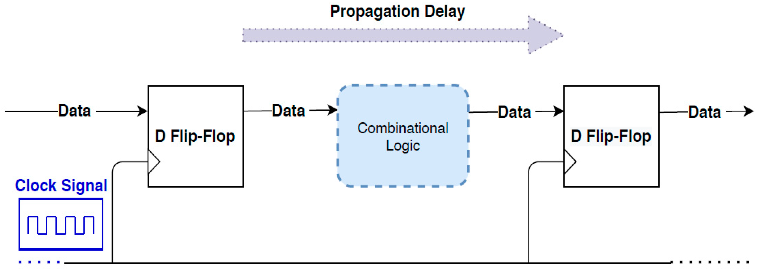
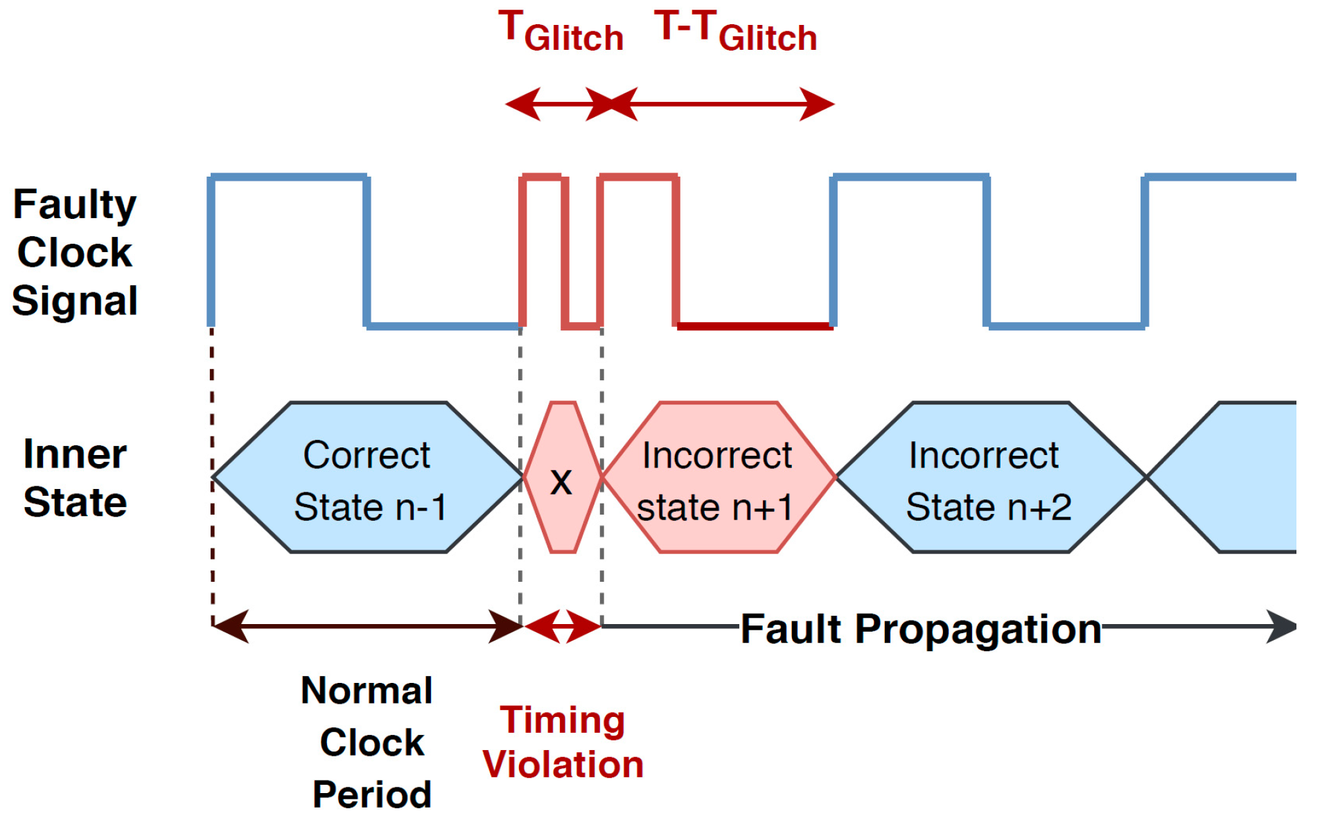
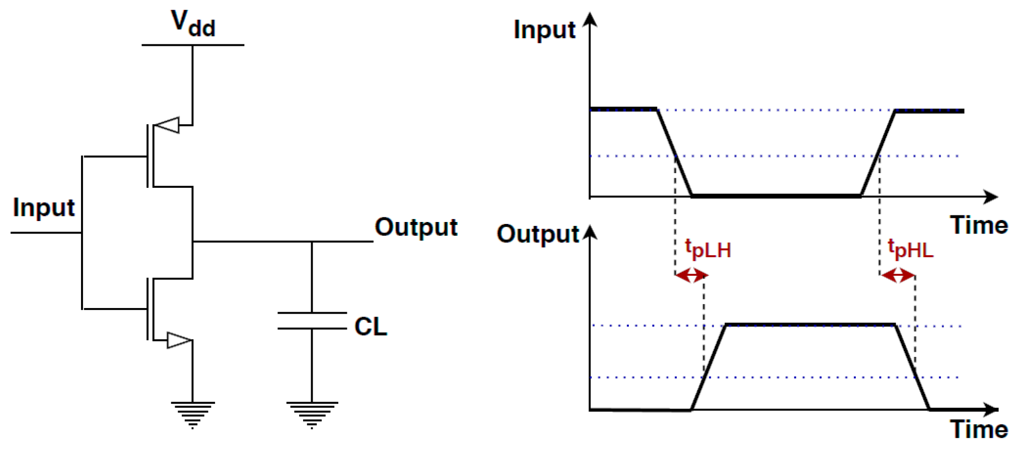
2.1.1. Clock Fault Injection Concept

First of all, to explore the importance of proper timing in digital ICs, one has to understand the synchronous design concept [39]. This is the basis for simple to complex computing systems. Digital designs often consist of two main parts: (1) combinational logic for computational operations and (2) memories such as register banks to store the computation results after each clock cycle. Figure 2 shows the concepts of the propagation delay and set-up time as irrevocable delays for performing computational operations. They are important timing parameters and need to have valid stored values in the flip-flops. The inequality in Equation (1) should be satisfied in order to guarantee the correct behavior of the flip-flop. In Equation (1), Tclk represents the clock period, Tcritical represents the minimum time needed to process the data through the combinational part, and Tset-up represents the set-up time of flip-flops, specified as the minimum amount of time for which data input needs to be stable before the active edge of the clock
Tclk > Tcritical + Tset-up
One way to perform fault injection attacks is to violate these timing constraints. Violation of the time constraints induces faults in the target. Tcritical and Tset-up are two fixed parameters that are defined based on the system logic design and cannot be manipulated to perform fault injection. Unlike the previous parameters, Tclk is a knob used for attackers to carry out their fault injections.
Clock fault injection is applied by tampering the clock signal temporarily or permanently. There are two different methods of clock fault injection: (1) overclocking and (2) clock glitch inducing. Overclocking is a kind of timing violation attack in which we try to apply a clock signal with a higher frequency than the nominal frequency for a specific time interval [39]. In fact, the overclocking method violates the timing constraint inequality (Equation (1)) by decreasing the clock period. Clock glitch is regarded as an unwanted transition in the clock signal. In the clock glitch inducing method, the attacker generates glitches in the clock signal. The induced glitches produce extra edges in the clock signal which can result in an erroneous output as the timing inequality has been violated. Figure 3 shows a typical clock signal in which a glitch is induced. In this figure, T represents the normal clock period, and TGlitch is the width of the glitch signal. As it can be seen, an extra edge appears in the clock signal. Another important parameter is Tmin, which is equal to the reciprocal of maximum frequency. In order to have erroneous behavior, TGlitch should be less than Tmin [39]. Moreover, in [27] the authors have considered ‘T-TGlitch’ as a ‘post-glitch’ phase. This abnormal semi-clock part could be considered as another approach for fault injection. In this case, if ‘T-TGlitch’ is less than Tmin, it leads to an erroneous behavior. Figure 4 shows how a clock glitch can inject faults in the system and how these faults can propagate through the next clock cycles [17].
Table 1 compares the accuracy of overclocking and clock glitch attacks. The first column entitled ‘spatial precision’ refers to the level of accuracy with which the fault generator can inject a fault into a specific location. Temporal precision, the second column, is defined as the accuracy of the fault injection process in inducing a fault at a specific time. The third column reveals glitching parameters such as frequency, width, and amplitude. The last two columns show equipment costs and the required level of expertise for fault injection, respectively. Since the clock is a global signal, we lack sufficient control to induce a fault in a specific location in the system. Consequently, fault induction in the clock signal would not have high spatial accuracy with either the overclocking or clock glitching techniques. In the clock glitching method, high temporal precision can be achieved by synchronization between the target and the fault generator circuit. Temporal precision is meaningless in the overclocking technique as the increase in clock frequency is considered as a fault. Briefly, the clock glitching technique is more desirable than the overclocking technique as it provides more accuracy and flexibility to manipulate clock signal parameters. In fact, the overclocking technique is not applicable for injecting a fault into a specific instruction at a specific time. In such cases, clock glitching is the only technique for fault attacks. For accurate fault attack using the clock glitching technique, especially for complex processor architectures employing the instruction pipeline, the fault generator circuit must be highly accurate in terms of injection time and location. In addition, the injection process should be carried out as fast as possible to avoid synchronization violations [42].
In this work, our main focus is on the clock glitching attack approach. Figure 5 shows a typical circuit employed by attackers to conduct a fault injection attack. A clock glitch generator generally consists of different hardware components such as FPGA boards, pulse generators, and microcontrollers to enable the implementation of various glitch generating methods. The desired configuration is provided by a controller PC connected to both target and generator sides. Synchronization is done by using the trigger signal between the target and the generator.

2.1.2. Clock Glitch Generator Characteristics

As mentioned earlier, fault generators, in general, should have specific characteristics, namely accuracy, run-time configuration, reproducibility, and randomness. In this sub-section, we discuss clock glitch generator characteristics. Below is a list of the main features which we will identify and then for each category we will compare the related articles in Section 3.
  • Clock glitch accuracy: This feature includes parameters such as minimum glitch width, gliding shift steps, standard deviation, clock glitching placement, and clock glitch frequency control. These features are dependent on the characteristics of the clock generator and the method used to induce the glitches.
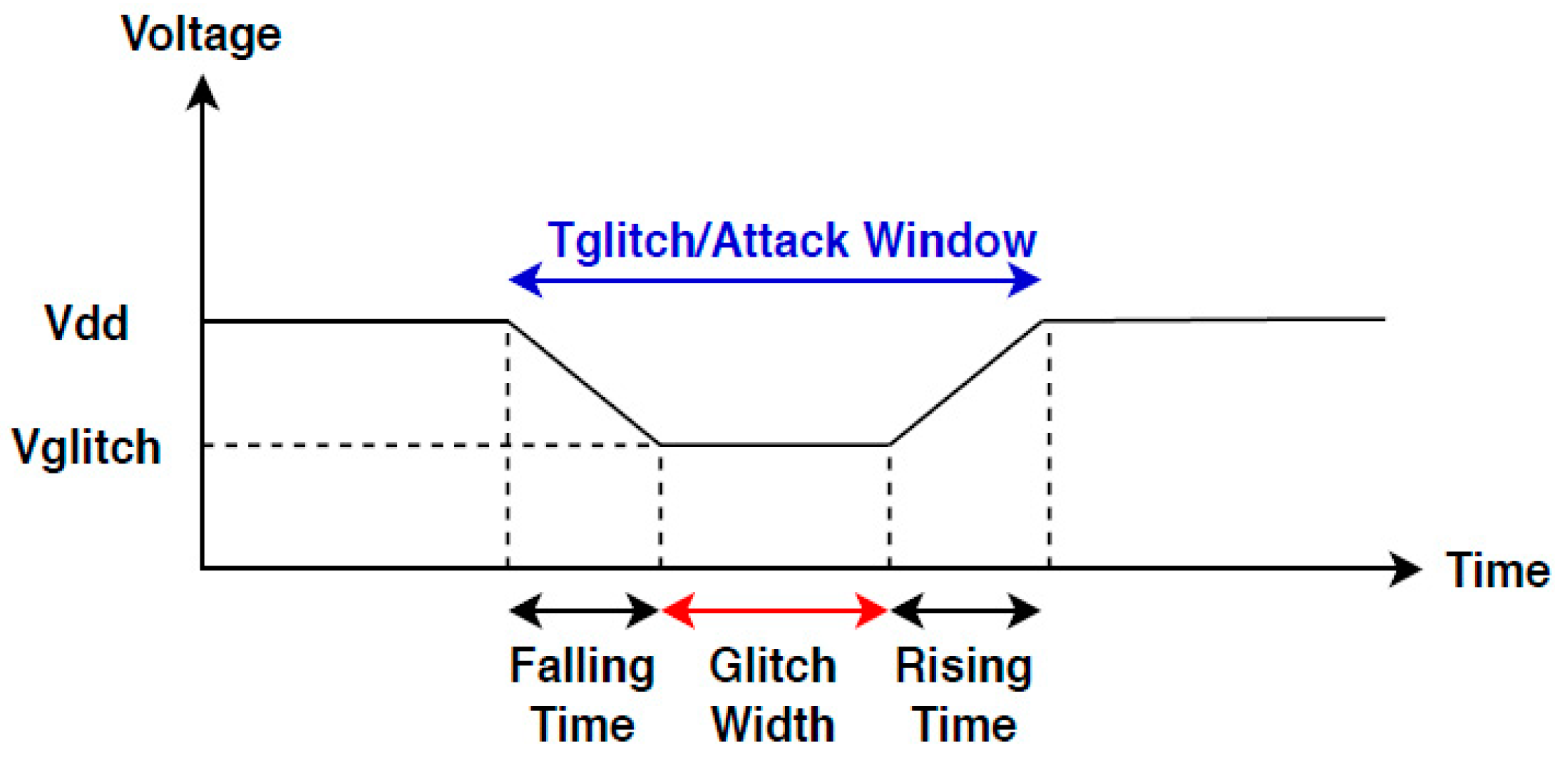
    • Minimum glitch width: Most target systems contain protocols to protect their external clock input so that when an abnormal clock is observed and detected, it resets the system or produces an alert. Therefore, less glitch width results in a lower chance of detection. In addition, in many cases, a precise and short glitch is needed to target a specific instruction running on the processor or specific data being fetched. This makes it important to control the glitch width. The precision of the clock glitch width is on the time scale of picoseconds or a few nanoseconds. For example, in Reference [41], a two-channel pulse generator has been used to design an accurate 35 ps glitch. Reference [11,40] and [42] include glitches on the nanosecond scale.
    • Gliding shift steps: this parameter refers to the minimum value by which a clock glitch generator adjusts the glitch width. These steps are on the nanosecond time scale. For example, in Reference [27,29], the gliding shift steps are reported as 1 ns.
    • Standard deviation: The standard deviation of the reported glitch width depends on the glitch generation algorithm and the limitations of the hardware used (e.g., FPGA).
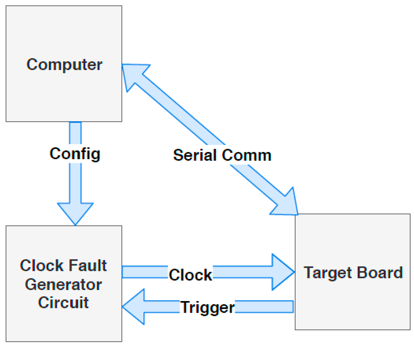
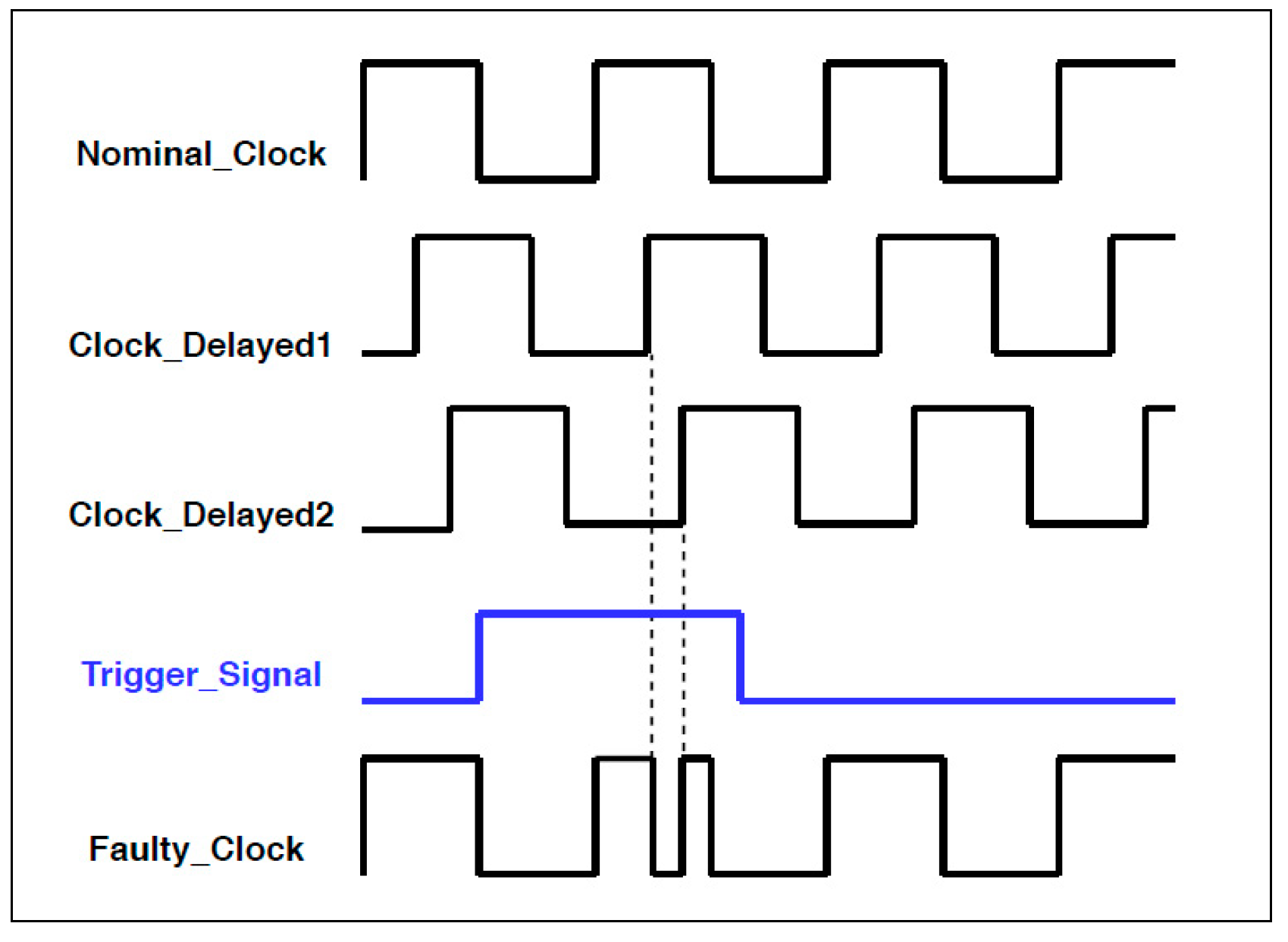
    • Clock glitching placement: It is important to induce a glitch into a specific position of the clock signal. For example, it is important to inject a glitch into a system at a certain round of encryption. Reference [40] uses a counter to determine the location of the glitch injection.
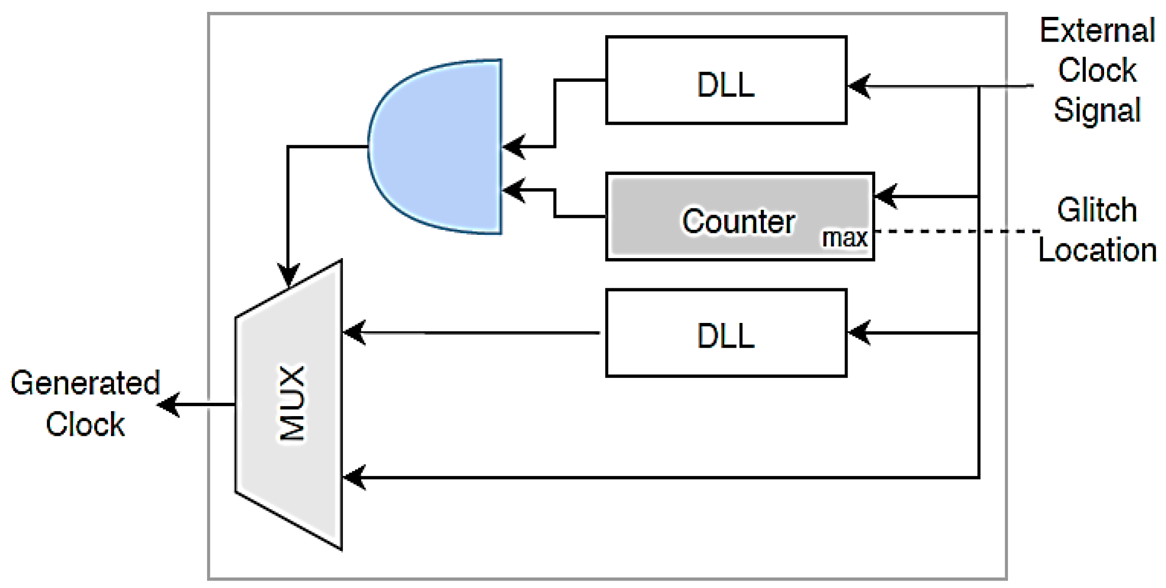
  • Clock glitch run-time configuration: Glitchy-clock parameters, such as phase delay and frequency, can be reconfigured at the run-time to help the attacker. For example, in [40], a digital clock manager (DCM) of an FPGA is used to configure the glitch. FPGA run-time adjustment can be used to change the phase-shifted values, but this method is limited to a certain range of values. Reference [19] presents an approach for partial configuration using the FPGA configuration capabilities, including reconfiguring the DCM blocks at the run-time. The ‘bit-stream differential files’ generated by FPGA tools are applied to substantiate the run-time configuration.
  • Clock glitch reproducibility: this helps attackers to reproduce the faulty clock signal with the same characteristics as many times as they wish. It is important in some applications, which require the assessment of vulnerabilities and tracking of the clock glitch attack procedure. Reference [41] includes a unique evaluation platform (SASEBO) for reproducible clock glitch generation.
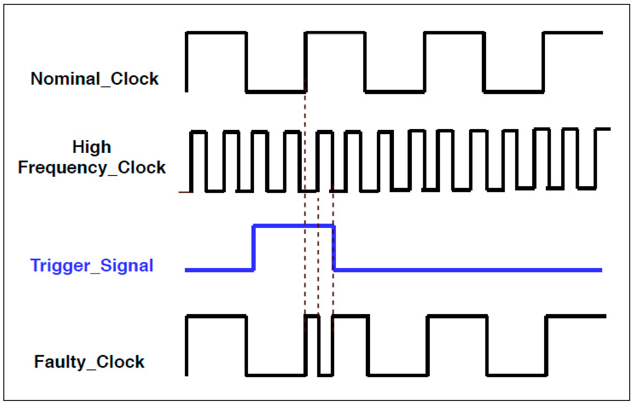
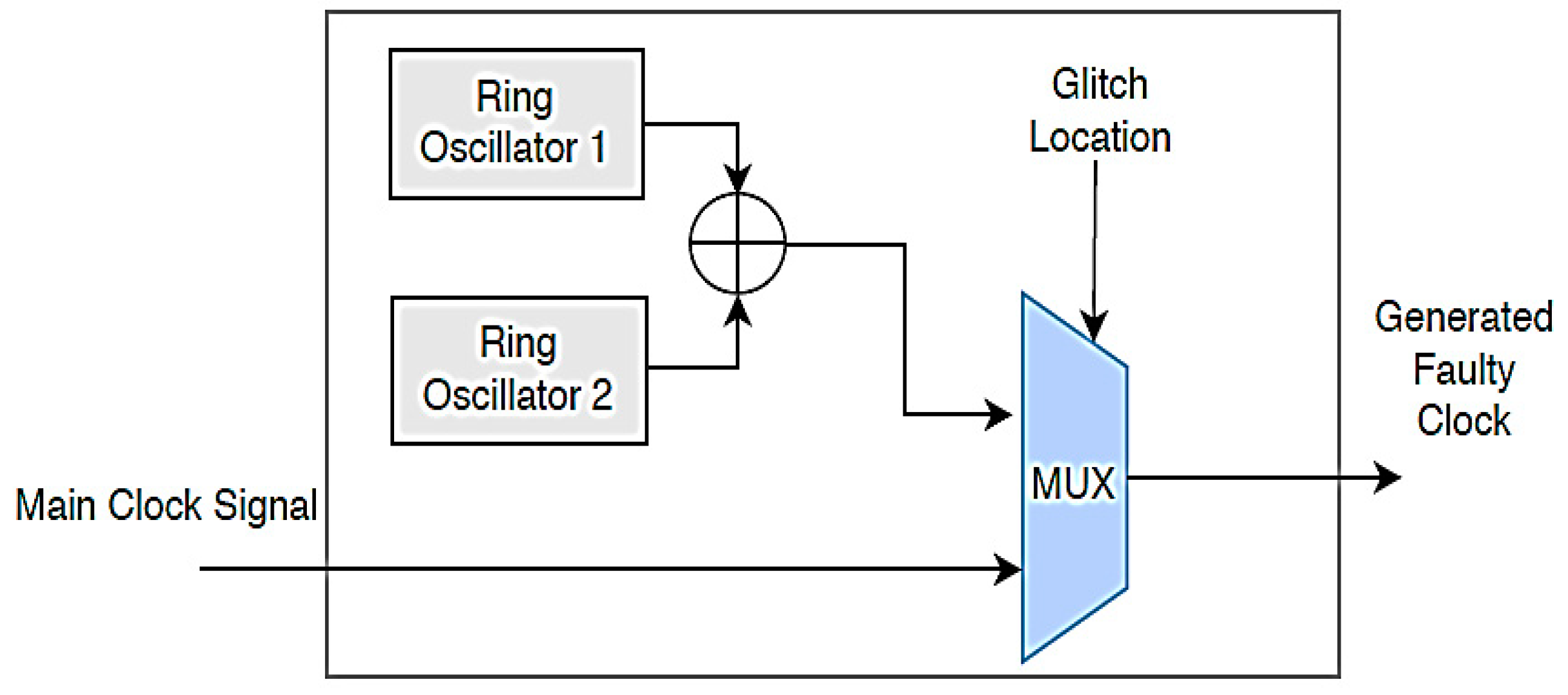
  • Clock glitch randomness: In most clock glitch generators, the glitch parameters—such as frequency, width, precision, etc.—are pre-determined, i.e., they are determined before run-time. This requires complete and adequate information about the target system, which would not be possible in all real-world attack scenarios. Furthermore, in order to have a highly efficient attack, one needs to cover a large number of possible combinations of the parameters mentioned, which would not be practical in a limited time. For this reason, in recent years, new techniques such as the fuzzy glitch generator have been proposed for the generation of clock glitches [38]. All of these techniques use ring oscillators instead of FPGA blocks and demonstrate the ability to achieve a highly successful attack rate. Details of the related works will be provided in the following section. In the next sub-section (Section 2.2.), we will discuss the basic set-ups and main characteristics of voltage glitch generators.

2.1.3. Clock Glitch Attack Examples

The clock glitching attack can have a significant impact on the critical parts of a running application such as its encryption module and arithmetic or logical instructions. In several works, a specific round or operation of the AES algorithm has been targeted by a clock glitching attack to generate faulty cipher text [11,27,33]. These faulty outputs can be used to recover the encryption key. Other than AES, other cipher blocks including DES, Camellia, CAST-128, SEED, and MISTY1 have been evaluated against clock glitching in [41]. To conduct a deep analysis of fault impacts, in [27] five commercial and low-cost processors have been targeted by clock glitch injection.

2.2. Voltage-Based Fault Attacks

Voltage fault injection is another practical and low-cost attack that can be used by adversaries to conduct efficient attacks against targeted systems employing one or multiple external voltage inputs. The fundamental concepts and related characteristics for this technique are provided in the following sub-sections.

2.2.1. Voltage Fault Injection Concept

An important class of voltage glitch attack is manipulation of supply voltage [7,9,28,29,32,43]. This is specifically applied in scenarios where the target system is fed from an external power supply [32]. Similar to clock fault attacks, voltage fault attack is an approach that does not require extensive equipment or knowledge. Moreover, it can be used when access to the external clock input is not available on the target systems, i.e., those using their own internal clocks.
The non-equality in Equation (1) points out the condition for correct circuit operation and correct value storage in memory. As mentioned previously, a straightforward approach to producing a timing constraint violation is to manipulate the clock period. The other approach to manipulate the timing constraint is to increase the data propagation delay by tampering the input voltage. In these approaches, Equation (1) will not fulfill the condition, which may result in erroneous data captured by memory cells and/or flip-flops. [44] discusses the relation between the input voltage and data propagation delay by a simple CMOS inverter as an example. Figure 6 shows that there are two propagation delays, named TpHL and TpLH for the output variations from high to low and vice versa.
Equation (2) reveals that these two parameters depend on different factors, including supply voltage. In this equation, Vdd is the power supply voltage, CL is load capacitance, Vth.p is PMOS threshold voltage, μp is holes mobility, Cox is gate oxide capacitance, and (Wp/Lp) is the aspect ratio of the PMOS. By replacing the parameters related to the inverter’s PMOS by NMOS parameters (e.g., μn, (Wn/Ln), Vth.n), TpHL can also be derived [44]. Equation (2) demonstrates that TpHL and TpLH have a direct relation with Vdd. In particular, reducing the power supply will increase TpHL and TpLH of the inverter. Therefore, manipulating the supply voltage (in long or short intervals) can be an efficient approach to inject a fault in order to violate the timing constraints [32,45].
T pHL = C L [ 2 | V th . p | V dd | V th . p | + ln   ( 3 4   | V th . p | V dd )   ] µ p   C ox   W p L P   ( v dd   | V th . p | )
There are two main types of voltage attacks: (1) underpowering and (2) voltage glitching [45]. Underpowering is a type of voltage manipulation in which the target’s supply voltage is applied permanently (or for a relatively long period) to a voltage source out of its nominal range (the standard voltages defined by the manufacturer). Voltage glitching is sudden and momentary changes in the supply voltage. It has been shown that underpowering is not sufficient to achieve a high success rate [12,23].
In voltage glitching, the attacker attempts to feed the target with a power supply below the considered nominal value for a certain period. Voltage glitching is generally used to induce a fault via timing violation; however, an attacker needs to have high control over the attack procedure and precision. This sudden (usually negative) change of voltage can induce transient faults. In this regard, a multiplexer can be used to switch the voltage between the two Vdd and Vdd -Vdiff values [10,28,29]. The value for Vdiffs strongly depends on the protection protocol that exists in the target system. If it goes beyond a certain value, such unusual behavior may trigger a warning regarding target system functionality and reliability, and usually leads to a device reset (to prevent damage in the IC, burning of electronic components, etc.). Typically, injected voltage glitches are generated as a square or V-shaped signal [32]. Figure 7 depicts an example of a negative voltage glitch. However, the amplitude of such a glitch can be positive (i.e., above the nominal voltage value) [45].
The shape of the glitch is defined by the rising and falling time (tf and tr) and the pulse width (tp). The sum thereof represents the total duration of the glitch, named tglitch [8,28,46]. Tglitch is also referred to as the attack window. This window is located between the falling and rising edges for negative glitch inducing and vice versa for positive. Vglitch is the voltage level that is fed at the target glitching time.
Table 2 compares the accuracy of underpowering and voltage glitching attacks. All the column headings are the same as those in Table 1 as described in the previous sub-section. The first column compares the spatial accuracies of underpowering and voltage glitching. The advantage of voltage fault injection methods as compared to clock fault injection methods is higher spatial accuracy (moderate level). The spatial precision of voltage fault injection is due to the presence of multiple power islands in modern systems. These systems typically operate in multiple power islands in accordance with their performance requirements. However, the temporal precision of voltage glitching (column 2) is less than that of clock glitching. In addition, the precision of the fault injection process in inducing a fault at a specific time is not applicable to the underpowering and overclocking approaches. The third column compares the attacker’s level of control over the voltage glitch parameters, such as glitch delay and width in voltage fault injection methods. The same level of control is not attainable for underpowering attacks. Finally, the last two columns show equipment costs and the required level of expertise for the two methods, which are very similar.
Based on the facts above, in this work, our main focus in voltage fault injection attacks is on the voltage glitching attack. Figure 8 shows a common set-up employed by attackers to conduct successful voltage glitching attacks. A voltage glitch generator generally consists of different hardware components such as power sources, FPGA boards, and high-speed multiplexers to enable the induction of the desired glitch shape(s) in the generated voltage signal. Similar to the clock fault injection set-up, a controller PC is connected to both target and generator sides to determine and configure the parameters of the attack. Synchronization is done by using the trigger signal between the target and the generator. The glitch may be injected by using a trigger signal from the general-purpose I/O pins and set up by running the program on the target.
Below, we will briefly examine and classify the main characteristics of voltage glitch generators.

2.2.2. Voltage Glitch Generator Characteristics

As mentioned in the previous sub-sections, different characteristics, namely accuracy, run-time configuration, reproducibility, and randomness, play an important role in successful fault injection attacks. In this sub-section, we will discuss these characteristics for the voltage glitch generators. There are many similarities between voltage and clock glitch generator characteristics. Here we will analyze each voltage glitch generation feature in more detail, and later compare the works related to these features in Section 3.
  • Voltage glitch accuracy: Various parameters can affect the accuracy of the generated voltage glitch, such as minimum glitch width, glitch delay, and glitch placement. These features are dependent on the characteristics of the voltage generator and the method used to induce the glitches.
    • Minimum glitch width: Generally, a precise and short voltage glitch is needed to bypass the existing glitch detectors on the external voltage inputs of the targeted systems. These protection modules observe the external voltage inputs and can reset the target system or create an alert to avoid any malfunction. Furthermore, a short voltage glitch is needed to target a specific instruction of the running code on the processor. Therefore, the more accurate and tenuous the voltage glitch is, the more chances an attacker has to accomplish the desired fault attacks. Depending on the equipment employed to generate the faulty signal, the minimum value of the glitch width can be changed. For instance, in the generator presented in [45], a pulse generator is used to generate the optimized voltage glitch, and the minimum pulse width is reported as 10 ns.
    • Glitch delay: This parameter shows the amount of time a voltage glitch takes to be injected after the setting up of the trigger signal [7]. To take advantage of the existing vulnerabilities in the running application, the glitch must be induced simultaneously with specific instruction(s) execution. According to the selected glitch width, the glitch delay should be considered to guarantee that the injected glitch hits the targeted instruction. For instance, to generate faulty ciphertexts, it is important to inject a glitch into the target at a certain round of encryption [47]. Other situations in which the glitch injection time is a crucial concern are escalating privileges [7], skipping authentications, and misinterpreting an instruction [8].
    • Voltage glitch placement: this parameter is related to the spatial position of the glitch. Spatial precision specifies the exact locations of the targeted circuit affected by the faulty voltage signal. In advanced systems such as modern SoCs, there are different power domains or power islands. A power domain is a group of gates powered by the same supplier. Depending on operational conditions, different voltage suppliers are connected to these domains. This parameter can help the attacker to provoke an erroneous behavior in a specific part. For example, by targeting an area in the chip like register banks and inducing memory faults, the wrong values may be gathered from the memory bus [21].
  • Voltage glitch run-time configuration: this parameter is defined as the possibility of reconfiguring the voltage glitch during the run-time. The parameters of generated glitchy voltage signals such as glitch width, delay, and amplitude can be reconfigured at the run-time to help the attacker to examine different attack scenarios. Run-time configurability depends on the specifications of the generator circuit. Reconfigurability can be applied through hardware inputs (e.g., by using sliding switches to adjust glitch width) or by communicating (e.g., UART) with the controller PC [19].
  • Voltage glitch reproducibility: This feature helps the attacker to obtain the same voltage glitching attack results when the same glitch is injected into multiple runs. Typically, voltage glitch generations are reproducible when fixed values are identified for the glitch parameters.
  • Voltage glitch randomness: Instead of pre-defining and pre-calculating all voltage glitch parameters in every attack scenario, an attacker can select them randomly from an interval of possible values. Using this approach, more combinations of the parameters mentioned can be covered within a short time, which leads to the conducting of more successful attacks. With some of the previously proposed approaches, such as [7], parameters such as glitch width and glitch delay are defined using a divide and conquer method with a randomized parameter approach. Now that we have categorized the important parameters of glitchers, in the next section, we will review some of the main works in the field.

2.2.3. Voltage Glitch Attack Examples

This type of attack has been employed against various critical modules of embedded applications. One of the most critical examples is the encryption module such as the AES algorithm which has been evaluated against voltage fault injection attacks. In this algorithm, applying voltage fault injection results in reduction of the number of encryption rounds [21]. The faulty cipher texts can be easily used to reveal the encryption key. Moreover, it has been used by an adversary to induce faults and bypass different security features such as the authentication or secure boot of the embedded systems. The induced fault can help the attacker to load his/her arbitrary values in the PC (program counter) register, which is very dangerous for secure systems [8]. Finally, Reference [7] has showed that the voltage glitching attack can lead to privilege escalation from the user to kernel mode in the Linux OS.

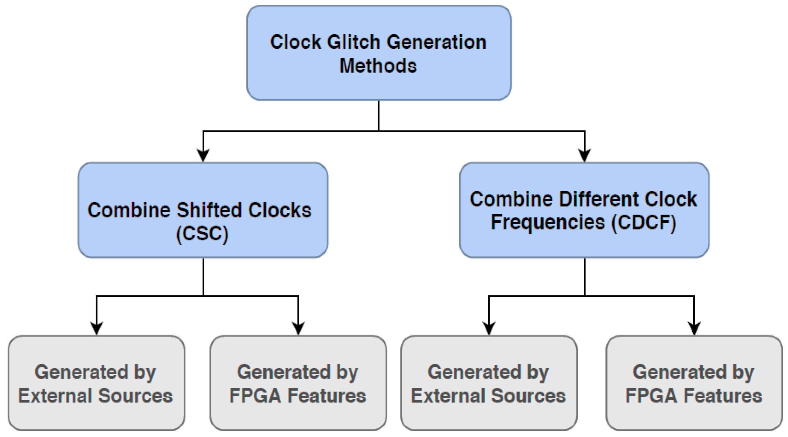
3. A Review of Previously Proposed Clock Glitch Generators

In this section, we review the previously proposed clock fault injector designs. We classify the previous works based on the parameters mentioned earlier in Section II. Then we compare them in terms of operational constraints, accuracy in the generated signal, and impacts on the target system. Table 3 shows the details of our comparison.
There are various practical techniques for generating a faulty clock signal [11,17,19,27,29,37,38,39,40,41,48,49]. All of the proposed methods call for a high-frequency clock signal, the so-called ‘Nominal Clock’ on the clock fault generator side. Nominal Clock generation can be done via several methods, including ring oscillator, phase-locked loop (PLL), voltage oscillator coupled with PLL and clock frequency circuit, or crystal oscillators. Figure 9 Summarizes the different solutions to generate a single glitch or even multiple glitches in the nominal clock signal. In this paper, we have classified the related works into two broad categories: (1) combine shifted clocks (CSC), (2) combine different clock frequencies (CDCF). Below, we introduce the works in each category. It should be noted that all previous works assume that the external clock of the target system is accessible.

3.1. Combine Shifted Clocks (CSC)

Combine shifted clocks (CSC) is based on multiplexing two different clock signals with the same frequencies and different phases at the appropriate time [39]. Figure 10 shows the point of multiplexing which is defined by the trigger signal (Clock_Delayed1 and Clock_Delayed2) [19,37,39,41]. In CSC, the glitch width and glitch period are controlled by the trigger and shifted clock signals.
In order to have higher accuracy and control over the glitch generation, [27] presents a method in which the output clock is created by multiplexing between three signals (rather than two) with equal frequencies and different phases.
There are mainly two implementation groups to produce the shifted versions of the nominal clock signal and to combine them. The first method is based on using external clock sources with phase-controlling capability. Figure 11 shows an example [41] that combines the two external clocks using a 2-to-1 multiplexer from a two-channel pulse generator. In the proposed glitch generator, the trigger signal is set to be synchronous with the execution of the running code on the target. To this end, an oscilloscope detects the positive edge of the target’s execution signal and then sends out the trigger signal with a constant delay.
The second method utilizes internal FPGA features such as the embedded DLL (delayed locked loop) to generate the shift [19,37,39,40]. In this method, the precision of the glitch is closely related to the smallest elementary delay of the DLL.
Figure 12 illustrates a method in which two DLLs and a counter are used to control the glitch delay [40]. Compared to [39], this method can change the glitch period in just one cycle and can induce glitches into any cycle (higher configurability).
Note that the frequencies of the generated clocks are limited to the DLL circuit of FPGA. To solve this issue, Reference [40] used dividers to output the desired frequency.

3.2. Combine Different Clock Frequencies (CDCF)

Combine different clock frequencies (CDCF) is based on multiplexing the nominal clock with a high-frequency clock of the same phase whose period is Tn and Tg, respectively [11,27,48]. Figure 13 demonstrates how a trigger signal is used for timely multiplexing between two clock signals in the CDCF-based method.
There are mainly two implementation approaches for CDCF. The first group is based on generating the desired clock signals using external sources [11,38]. For example, [11] uses a wave generator to produce the nominal clock and the high-frequency clock. However, this approach cannot provide an acceptable level of randomness in clock glitching scenarios. Reference [38] introduces an approach that includes randomness in the glitch generation procedure named fuzzy glitching. This approach is based on the use of adjustable ring oscillators at various frequencies. In this work, instead of producing exactly timed glitches, random glitches are made by using ring oscillators. Figure 14 shows an application of fuzzy glitching where a multiplexer is used to inject the glitches into the system for a limited time.
The second approach is based on generating the clock signals with different frequencies by using the interior FPGA features such as phase locked loop (PLL). As an example, in Reference [48], a precise and accurate external clock signal passes through the on-chip PLL to provide the appropriate nominal clock. The unchanged version of that external clock signal is used to produce the faster clock. Multiplexing between these signals can be performed via mixed mode clock management (MMCM).
Table 3 summarizes the technical attributes of the proposed CSC-based and CDCF-based clock glitch generators. Table 3 shows that in both CSC and CDCF, clock glitches are either generated using internal features of FPGAs or by external clock sources. FPGAs are the major platform for clock glitching experiments [19,27,37,38,39,41]. A waveform generator is also a common tool used in CDCF to generate a high-frequency clock signal. Below, we elaborate on all of the parameters reported in Table 3.
Table 3 compares different approaches in terms of complexity and cost. It shows that the FPGA-based approaches are easy to implement and very cost-effective [19,27,39]. There are generators that require custom board design and need to be produced by more skilled engineers and perhaps at a higher cost. Moreover, there are specific evaluation boards such as SASEBO and Chipwhisperer which are semi-configurable and have a moderate cost [18,19,20].
Table 3 reports the minimum glitch width values and studies the fault clock cycle location among different approaches. It is observed that [19] from the CSC category and [11] from the CDCF category provide the most precise glitches among different glitch generators. It also shows that all the previous works, except the fuzzy generator [38], have the capability to inject glitches in the chosen clock cycle [19,27,29,37,39,40,41].
Another important factor for fault generators is the run-time configuration. Table 3 shows the limitation of this factor in FPGA-based generators [27,29,37,39,40,41]. The design in [19] uses a more advanced Xilinx board and can, therefore, support more runtime configuration parameters such as glitch delay and glitch width. Finally, Table 3 analyzes the clock glitching approaches with respect to reproducibility and frequency adjustability. All of the glitch generators, except [38], can reproduce any faulty clock signal with exactly the same characteristics. Instead, the capability of providing random faulty clock signals is only considered in [38]. Clock frequency adjustments are also possible for all of the reviewed generators. However, FPGA’s clock management units create another limitation related to the generated clock maximum frequency [19,29,37,39]. This setting is less restricted using external clock resources [11].

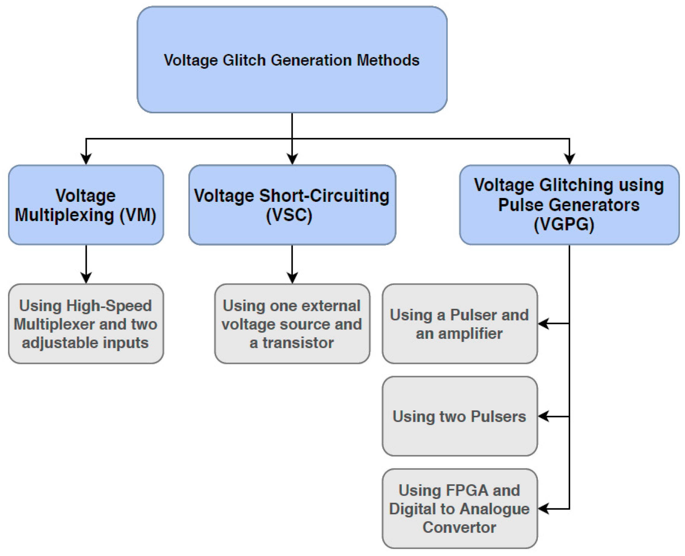
4. A Review of Previously Proposed Voltage Glitch Generators

In this section, we review the existing voltage fault injector designs. The parameters discussed in Section 2 are used to compare them in terms of operational constraints, accuracy in the generated signal, and impacts on the target system. The comparison results are then presented in Table 4.
The input voltage of a target system can be manipulated to perform fault injection if the system is connected to an external source. Reducing the input voltage increases the propagation delay, and can result in timing violations [44]. Voltage fault injection can be performed either by permanently decreasing the voltage supply (underpowering) [9,32] or by multiplexing between different voltage levels for a limited time (voltage glitching) [7,8,45,50].
For the underpowering method, adjusted, and pre-planned parameters are not required. Instead, in order for an attack to be performed, the target simply needs to be connected to a constant voltage below the nominal voltage. However, this value depends on the target system specifications and occasionally calls for many trials and errors in order to be found [47]. For example, to perform differential fault attacks (DFA) using this approach, the attacker must find a particular voltage at which the faulty output would appear. Furthermore, the applied voltage should be above a threshold value at which the target system is functional, and communications to the controller computer must operate in order to collect the faulty outputs [9,23,44].
Although underpowering is a low-cost and simple method to implement, it does not provide the required time and location precision in many attack scenarios [10,32]. For more effective attacks, voltage glitch fault injection is employed. To obtain the desired voltage signal and to induce faults in the target systems accurately, different implementations are employed. Figure 15 summarizes the main techniques for voltage glitching.
Figure 15 shows the classification of the related works into three categories: (1) voltage multiplexing (VM); (2) voltage short-circuiting (VSC); and (3) voltage glitching using pulse generators (VGPG).
It should be noted that for a more effective attack, some changes may be made to the experimental set-up before voltage fault injection is performed. For instance, the main power supply from the target chip should be disconnected. This calls for the removal of the corresponding resistor bridge, which helps to control the voltage supply of the target system. Moreover, all existing bypass capacitors on the target PCB should be detached since their role is to enhance stability, and they are not needed to carry out the attack process. Below, we introduce the works in different categories.

4.1. Voltage Multiplexing (VM)

VM is based on the use of a high-speed multiplexer to switch between Vdd and a lower voltage value during trigger signal activation [10,32]. In Reference [10], one high-speed multiplexer on an FPGA is used. The multiplexer includes two adjustable inputs, and its output is connected to the target system in order to switch between different voltage levels (Vdd and 0 volts).
To select a proper multiplexer for the fault injection set-up, there are different specifications to be considered, including input voltage limits, switching speed, output leakage, existing capacitance, and charge injection. Depending on the required voltage ranges on the output, different multiplexers are designed and optimized. Consequently, the proper multiplexer should be used in order to avoid performance degradation.

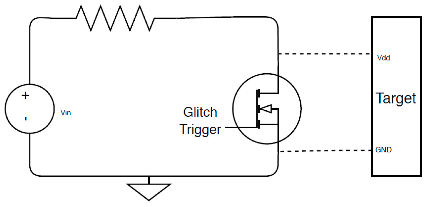
4.2. Voltage Short-Circuiting (VSC)

VSC is one of the most commonly-used fault injection approaches for generating one or multiple glitches in the voltage signal. Figure 16 presents the related set-up in which a transistor is placed in parallel to the power supply line in order to create a short-circuit between the Vcc and the ground [19]. In this method, additional equipment is required to control the voltage levels and the timing of glitch induction. The generated glitch can be erratic due to process variations and the target system’s electronic properties. Reference [32] has shown the oscillations in the generated voltage signal by using the VSC set-up and has proposed a method for a more precise and optimized voltage glitch shape.

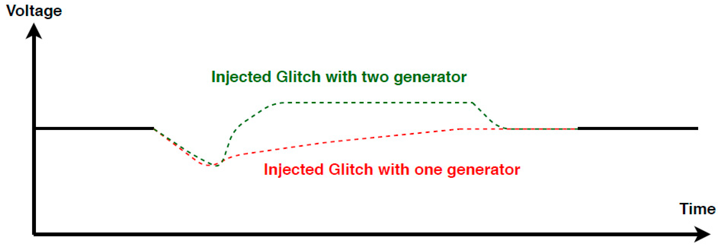
4.3. Voltage Glitching using Pulse Generators (VGPG)

The idea behind VGPG is to utilize a pulse generator as a DC voltage source to generate and inject arbitrary glitches (usually square shapes) into the supply path [8,32,44,45]. The pulse generator can produce the equivalent analog signal from a digital source [32]. A logic level change in the external input trigger leads to a transition from the constant supply voltage to the glitch waveform loaded in the generator. In Reference [32], a pulse generator is used to generate arbitrary waveforms in which a set of parameters can be defined at the software level and saved in the internal memory of the pulse generator. Reference [44] presents a solution for using two pulse generators (instead of one) to achieve higher precision. The second pulse generator can improve the generated glitch shape, and it brings the voltage value to the normal level at a higher rate. Figure 17 depicts the expected and altered glitches with one and two generators in this work. A high-speed FPGA can also be used to generate the desired pulse. In [8], an FPGA and an amplifier are used to produce the faulty voltage signal. In this case, glitch parameters are easily configured by loading the bitstream file into the FPGA.
Table 4 reviews voltage glitch generators and summarizes their technical features. The table compares the VM, VSC, and VGPG approaches and presents their implementation platforms (FPGAs, transistors, and pulse generators) [10,19,32,44,45,50,51]. Various targets and applications are also listed in the table and have been examined with respect to voltage glitch generators.
Complexity and cost are the first two parameters in our comparison shown in Table 4. It can be seen that most voltage glitching platforms can be implemented with moderate knowledge and expenses.
The minimum glitch width is the next parameter to consider in different voltage glitch generators. It depends highly on the equipment used and its ability to shape the precise voltage glitch. The VM-based approach could ideally generate very short glitches by internal FPGAs, however, due to the limitations on I/O pins or other connectors used, higher values are obtained in practice [10,51]. In the VGPG-based approach, the minimum glitch width is reliant on the capabilities of the pulse generator. For example, in Reference [45], it has been reported as 10 ns.
The next main parameter of voltage glitch generators is run-time configuration capability, which is limited to the MUX used in VM-based generators [10,51]. However, this setting is less restricted by the use of external voltage resources in VSC and VGPG approaches [8,19,32,44,50]. This table also shows that in all studied works, synchronization between the voltage glitch generator and the target is applicable by using a trigger signal.
As a final point, Table 4 analyzes the voltage glitching approaches concerning reproducibility. It shows that all of the glitch generators can reproduce any faulty voltage signal with the same characteristics. Note that these voltage generators cannot provide any random faulty voltage.

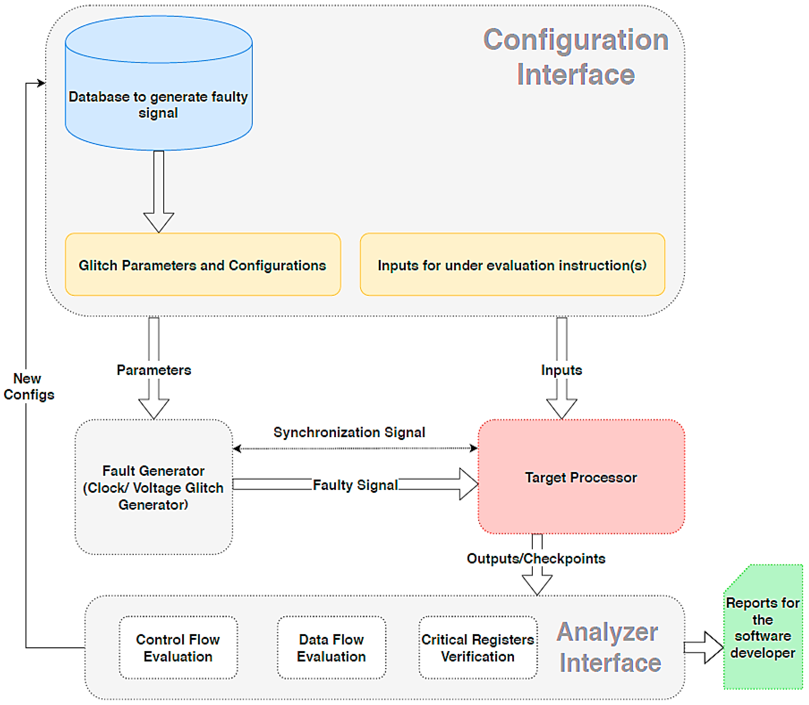
5. Characteristics of an Efficient Evaluation Platform for IoT Software Developers

In this section, we define the related characteristics of an ideal clock and voltage glitch generators according to the studied works in Section 3 and Section 4. Note that none of the platforms presented can attain all of the characteristics required to be an ideal one. Each of the glitch generators is highly dependent on the targeted application, existing hardware-based protections, and how widely the evaluation process aims at discovering the potential vulnerabilities. Our goal is to present a platform that can evaluate the MCU-based system against fault attack vulnerabilities within the software. This type of platform is easy to use and can provide acceptable precision for software evaluation by clock/voltage glitches. Figure 18 presents an example of a fault injection framework. Such a platform consists of a configuration interface which adjusts the fault parameters and sends the proper inputs to the target. Then, these parameters are used by a glitch generator and applied to the target. The corresponding fault injection attack results are evaluated in the analyzer interface and generate a report that can be used by the embedded software developer. Our focus in this paper has been on the glitch generation part and in the following various design considerations for glitch generators are presented.

5.1. Clock Glitch Generator

The main criteria in the design of an efficient clock glitch generator are the devices used, complexity, and cost. FPGA development boards are one of the electronic platforms which can be used to build less complex and low-cost clock glitch generators. Table 3 compared various development boards used to design an appropriate clock glitch generator and presented the main factors accordingly.
Regarding this and to introduce clock glitchers, it is required to generate signals with shifted phases or different frequencies, which were described in the CDC and CDCF approaches. The generated clock glitch can change the behavior of the system and cause malfunction. Various FPGA types can be used to generate clock glitch(es). One desirable feature is the digital clock management (DCM) of the older and lower-cost FPGA models such as Spartan-3 and Virtex-4 or by the phase locked loop (PLL) of the newer models such as Virtex-5 and Spartan-6 [52]. Moreover, one can utilize the mixed-mode clock manager (MMCM) in Virtex-6 and the seven series FPGAs [53], which include both the DCM and PLL features. The advantage of using MMCM is that it can generate multiple accurate clock signals with defined shifted-phases or divided/multiplied frequencies.
Another design parameter to consider is the run-time configuration. This feature allows the user to modify the glitch characteristics without re-programming the whole system and can be especially useful in a testing scenario with various parameters. Reference [53] presents an example where different clock glitch generator parameters, such as output frequency, phase, and duty cycle, can be dynamically reconfigured effortlessly in the run-time. This utility is present in the Xilinx® 7 series, UltraScale™, and UltraScale+™ and is named the dynamic reconfiguration port (DRP).
Finally, the next main parameter of a clock glitch generator is its accuracy. Among the existing approaches, both the CSC and CDCF methods can produce very accurate glitches. However, the CSC approach has more parameters to control than the CDCF method does. For instance, with the CSC method, the glitch delay can be manipulated inside any single clock. Moreover, much thinner glitches can be produced by applying the CSC method due to the existing DLL constraint of generating higher frequencies for the CDCF method. As an example, [33] reported that the minimum glitch width with CSC is less than that with the CDCF method.
It should be emphasized that embedded software evaluation against clock glitching is a kind of practice that requires consideration of all the possible vulnerable instructions; therefore, manual adjustment of glitch parameters would not make sense. In this respect, automation of the clock glitch design in order to produce and induce the glitch in all clock cycles during the targeted software process is well-suited for glitch injectors and will be handy and practical for software assessments.

5.2. Voltage Glitch Generator

An efficient voltage glitch generator needs to be financially and technically viable for the IoT software developer. Therefore, this sub-section discusses some of the key trade-offs when designing a voltage glitch generator concerning the targeted software and hardware.
The complexity, cost, and accuracy of generated glitches should be considered in voltage glitch generator design. Table 4 presented different approaches and compared them in terms of cost. The VSC method is the cheapest approach with the least precision and adjustability, while the VGPG approach contains more expensive instruments and can produce very accurate glitches in comparison with the VSC method [32]. On the other hand, the cost of the VM method falls between the costs of the VGPG and VSC methods and requires a medium level of FPGA programming knowledge to produce voltage glitches that are sufficiently accurate for testing IoT devices.
The next design parameter to consider is glitch adjustability and run-time reconfiguration capability. The VSC is easier to implement than the VM method; however, the latter has more adjustable glitch parameters and capabilities. The use of the VM method on a modern FPGA, such as Xilinx series 6 and above [52,54], can greatly empower the inducing of the looked-for faults in the targeted application. For instance, it reduces the testing time due to the capability of developing automated testing scenarios with a large set of glitch parameters on the FPGA. Moreover, very short glitches can be generated by integrating digital pattern generators [55].
Another characteristic of a voltage glitch generator could be the capability to create glitches with negative values. Additional electronic components would be required to produce such voltages. The VGPA can generate such glitches. It uses one or more pulse generator chips to create glitches with negative voltage values.
In brief, for a voltage glitch generator with the highest configurability and adjustability, the VM method can be implemented and utilized on an advanced FPGA board. Then, if the glitch generator needs to include negative values, the extra circuitry can be added to the evaluation platform [13].

6. Conclusions

In this paper, two different approaches of experimental fault injection attack have been studied to help hardware security specialists to develop a proper and efficient evaluation platform. Thereafter, this platform can be used by embedded software developers. This evaluation platform can help them to make their applications robust against low-cost but effective physical attacks. Accordingly, we have reviewed the previously proposed clock and voltage glitch generators and categorized them based on different parameters that play an important role in the attack process.
The effectiveness of the fault injection approaches and the affordable equipment costs motivate the designers to propose clock and voltage fault injectors with optimum characteristics. Furthermore, most of the important factors—such as complexity, cost, and required knowledge—were discussed, leaving the final decision to be made by the hardware security specialists in consideration of these factors.
The fault injection attacks are becoming more advanced and complicated. This is mainly due to more accessibility of the software and hardware of embedded systems in IoT applications. Moreover, using artificial intelligence (AI) to learn and predict the fault injection parameters can lead to more successful attacks. On the other hand, the countermeasures need to be based on hardware-software co-design approach to reduce the bottlenecks between the design of independent hardware and software. Furthermore, the countermeasures can be strengthened by using a fault injection database pattern that helps the software developers to recognize vulnerable software and to apply the security patch.

Author Contributions

Conceptualization, Z.K.; methodology, Z.K., D.H., M.F. and V.B.; investigation, Z.K.; writing—original draft preparation, Z.K.; writing—review and editing, Z.K., D.H., M.F. and V.B.; supervision, D.H., M.F. and V.B.; project administration, D.H. and V.B.; funding acquisition, D.H. and V.B. All authors have read and agreed to the published version of the manuscript.

Funding

This work is supported by the French National Research Agency in the framework of the “Investissements d’avenir” program (ANR-15-IDEX-02). This work is carried out under the SERENE-IoT project, a project labeled within the framework of PENTA, the EUREKA cluster for Application and Technology Research in Europe on Nano Electronics.

Conflicts of Interest

The authors declare no conflict of interest.

References

  1. Thakar, A.T.; Pandya, S. Survey of iot enables healthcare devices. In Proceedings of the International Conference on Computing Methodologies and Communication, ICCMC 2017, Erode, India, 18–19 July 2017; pp. 1087–1090. [Google Scholar] [CrossRef]
  2. Xu, T.; Wendt, J.B.; Potkonjak, M. Security of IoT Systems: Design Challenges and Opportunities. In Proceedings of the 2014 IEEE/ACM International Conference on Computer-Aided Design (ICCAD), San Jose, CA, USA, 2–6 November 2014; pp. 417–423. [Google Scholar] [CrossRef]
  3. Yang, Y.; Wu, L.; Yin, G.; Li, L.; Zhao, H. A Survey on Security and Privacy Issues in Internet-of-Things. IEEE Internet Things J. 2017, 4, 1250–1258. [Google Scholar] [CrossRef]
  4. Deogirikar, J. Security Attacks inIoT: A Survey. In Proceedings of the 2017 International Conference on I-SMAC (IoT in Social, Mobile, Analytics and Cloud) (I-SMAC), Palladam, India, 10–11 February 2017; pp. 32–37. [Google Scholar] [CrossRef]
  5. Borgohain, T. Survey of Security and Privacy Issues of Internet of Things. arXiv 2015, arXiv:1501.02211. [Google Scholar]
  6. Lu, Y.; Xu, L. Da Internet of Things (IoT) Cybersecurity Research: A Review of Current Research Topics. IEEE Internet Things J. 2018, 4662. [Google Scholar] [CrossRef]
  7. Timmers, N. Escalating Privileges in Linux using Voltage Fault Injection. In Proceedings of the 2017 Workshop on Fault Diagnosis and Tolerance in Cryptography (FDTC), Taipei, Taiwan, 25 September 2017. [Google Scholar] [CrossRef]
  8. Timmers, N.; Spruyt, A.; Witteman, M. Controlling PC on ARM Using Fault Injection. In Proceedings of the 2016 Workshop on Fault Diagnosis and Tolerance in Cryptography (FDTC), Santa Barbara, CA, USA, 16 August 2016; pp. 25–35. [Google Scholar] [CrossRef]
  9. Barenghi, A.; Bertoni, G.; Parrinello, E.; Pelosi, G. Low voltage fault attacks on the RSA cryptosystem. In Proceedings of the 2009 Workshop on Fault Diagnosis and Tolerance in Cryptography (FDTC), Lausanne, Switzerland, 6 September 2009; pp. 23–31. [Google Scholar] [CrossRef] [Green Version]
  10. Martín, H.; Korak, T.; Millán, E.S.; Hutter, M. Fault Attacks on STRNGs: Impact of Glitches, Temperature, and Underpowering on Randomness. IEEE Trans. Inf. Forensics Secur. 2015, 10, 266–277. [Google Scholar] [CrossRef]
  11. Qiao, Y.; Lu, Z.; Liu, H.; Liu, Z. Clock Glitch Fault Injection Attacks on an FPGA AES Implementation. J. Electrotechnol. Electr. Eng. Manag. 2017, 1, 23–27. [Google Scholar]
  12. Piscitelli, R.; Regazzoni, F. Fault attacks, injection techniques and tools for simulation. In Hardware Security and Trust; Springer: Cham, Switzerland, 2015; pp. 15–20. [Google Scholar] [CrossRef]
  13. Kazemi, Z.; Papadimitriou, A.; Hely, D.; Fazeli, M.; Beroulle, V. Hardware Security Evaluation Platform for MCU-based Connected Devices: Application to healthcare IoT. In Proceedings of the 3nd International Verification and Security Workshop (IVSW), Costa Brava, Spain, 2–4 July 2018. [Google Scholar]
  14. Le Bouder, H.; Thomas, G.; Lashermes, R.; Linge, Y.; Robisson, B.; Tria, A. An Evaluation Tool for Physical Attacks. In Ad-hoc, Mobile, and Wireless Networks; Lecture Notes in Computer Science; Springer International Publishing: Cham, Switzerland, 2018. [Google Scholar]
  15. Thillard, A.; Prouff, E.; Roche, T. Success through confidence: Evaluating the effectiveness of a side-channel attack. In Lecture Notes in Computer Science (Including Subseries Lecture Notes in Artificial Intelligence and Lecture Notes in Bioinformatics); Springer Science+Business Media: Berlin, Germany, 2013; Volume 8086 LNCS, pp. 21–36. [Google Scholar] [CrossRef]
  16. Eslami, M.; Ghavami, B.; Raji, M.; Mahani, A. A survey on fault injection methods of digital integrated circuits. Integration 2020, 71, 154–163. [Google Scholar] [CrossRef]
  17. Potestad-Ordonez, F.E.; Jimenez-Fernandez, C.J.; Valencia-Barrero, M. Vulnerability Analysis of Trivium FPGA Implementations. IEEE Trans. Very Large Scale Integr. (VLSI) Syst. 2017, 25, 3380–3389. [Google Scholar] [CrossRef]
  18. Matsubayashi, M.; Satoh, A.; Ishii, J. Clock glitch generator on SAKURA-G for fault injection attack against a cryptographic circuit. In Proceedings of the 2016 IEEE 5th Global Conference on Consumer Electronics (GCCE 2016), Kyoto, Japan, 11–14 October 2016; pp. 5–8. [Google Scholar] [CrossRef]
  19. Chipwhisperer Side Channel and Fault Injection Attacks Tool Chain. Available online: https://chipwhisperer.readthedocs.io/en/latest/tutorials.html (accessed on 14 July 2020).
  20. Katashita, T.; Hori, Y.; Sakane, H.; Satoh, A. Side-Channel Attack Standard Evaluation Board SASEBO-W Specification Niat 2012. Available online: https://csrc.nist.gov/csrc/media/events/non-invasive-attack-testing-workshop/documents/10_katashita.pdf (accessed on 14 July 2020).
  21. Karaklaji, D. Hardware Designer’s Guide to Fault Attacks. IEEE Trans. Very Large Scale Integr. (VLSI) Syst. 2013, 21, 2295–2306. [Google Scholar] [CrossRef] [Green Version]
  22. Yuce, B.; Schaumont, P.; Witteman, M. Fault Attacks on Secure Embedded Software: Threats, Design, and Evaluation. J. Hardw. Syst. Secur. 2018, 111–130. [Google Scholar] [CrossRef] [Green Version]
  23. Selmane, N.; Guilley, S.; Institut, T. Practical Setup Time Violation Attacks on AES Jean-Luc DANGER. In Proceedings of the 2008 Seventh European Dependable Computing Conference, Kaunas, Lithuania, 7–9 May 2008; pp. 91–96. [Google Scholar] [CrossRef]
  24. Barenghi, B.A.; Breveglieri, L.; Koren, I.; Ieee, F.; Naccache, D. Fault Injection Attacks on Cryptographic Devices: Theory, practice, and countermeasures. Proc. IEEE 2012, 100, 3056–3076. [Google Scholar] [CrossRef] [Green Version]
  25. Li, Y.; Chen, M.; Wang, J. Introduction to Side-Channel Attacks and Fault Attacks. In Proceedings of the 2016 Asia-Pacific International Symposium on Electromagnetic Compatibility (APEMC), Shenzhen, China, 17–21 May 2016; pp. 573–575. [Google Scholar] [CrossRef]
  26. Moukarzel, M.; Eisenbarth, T.; Sunar, B. μleech: A side-channel evaluation platform for IoT. In Proceedings of the 2017 IEEE 60th International Midwest Symposium on Circuits and Systems (MWSCAS), Boston, MA, USA, 6–9 August 2017; pp. 25–28. [Google Scholar] [CrossRef]
  27. Balasch, J.; Gierlichs, B.; Verbauwhede, I. An in-depth and black-box characterization of the effects of clock glitches on 8-bit MCUs. In Proceedings of the 2011 Workshop on Fault Diagnosis and Tolerance in Cryptography (FDTC 2011), Nara, Japan, 28 September 2011; pp. 105–114. [Google Scholar] [CrossRef] [Green Version]
  28. Beringuier-boher, N.; Hely, D. Voltage Glitch Attacks on Mixed-Signal Systems. In Proceedings of the 2014 17th Euromicro Conference on Digital System Design, Verona, Italy, 27–29 August 2014; pp. 379–386. [Google Scholar] [CrossRef]
  29. Korak, T.; Hoefler, M. On the effects of clock and power supply tampering on two microcontroller platforms. In Proceedings of the 2014 Workshop on Fault Diagnosis and Tolerance in Cryptography (FDTC 2014), Busan, Korea, 23 September 2014; pp. 8–17. [Google Scholar] [CrossRef]
  30. Liao, N.; Cui, X.; Liao, K.; Wang, T.; Yu, D.; Cui, X. Improving DFA attacks on AES with unknown and random faults. Sci. China Inf. Sci. 2017, 60, 1–14. [Google Scholar] [CrossRef]
  31. Dusart, P.; Letourneux, G.; Vivolo, O. Differential Fault Analysis on A.E.S. In International Conference on Applied Cryptography and Network Security; Zhou, J., Yung, M., Han, Y., Eds.; Springer: Berlin/Heidelberg, Germany, 2003; pp. 293–306. [Google Scholar]
  32. Bozzato, C.; Focardi, R.; Palmarini, F. Shaping the Glitch: Optimizing Voltage Fault Injection Attacks. IACR Trans. Cryptogr. Hardw. Embed. Syst. 2019, 2019, 199–224. [Google Scholar] [CrossRef]
  33. Kazemi, Z.; Papadimitriou, A.; Souvatzoglou, I.; Aerabi, E.; Ahmed, M.M.; Hely, D.; Beroulle, V. On a Low Cost Fault Injection Framework for Security Assessment of Cyber-Physical Systems: Clock Glitch Attacks. In Proceedings of the 2019 IEEE 4th International Verification and Security Workshop (IVSW), Rhodes Island, Greece, 1–3 July 2019; pp. 7–12. [Google Scholar] [CrossRef]
  34. Guillen, O.M.; Gruber, M.; De Santis, F. Low-Cost Setup for Localized Semi-invasive Optical Fault Injection Attacks. In International Workshop on Constructive Side-Channel Analysis and Secure Design; Guilley, S., Ed.; Springer International Publishing: Cham, Switzerland, 2017; pp. 207–222. [Google Scholar]
  35. Sanlyde, D.; Skorobogatov, S.; Anderson, R.; Quisquater, J.-J. On a new way to read data from memory. In Proceedings of the First International IEEE Security in Storage Workshop, Greenbelt, MD, USA, 11 December 2002; pp. 65–69. [Google Scholar]
  36. Breier, J.; Jap, D. A survey of the state-of-the-art fault attacks. In Proceedings of the 2014 International Symposium on Integrated Circuits (ISIC), Singapore, 10–12 December 2014; pp. 152–155. [Google Scholar]
  37. Korak, T.; Hutter, M.; Ege, B.; Batina, L. Clock glitch attacks in the presence of heating. In Proceedings of the 2014 Workshop on Fault Diagnosis and Tolerance in Cryptography (FDTC 2014), Busan, Korea, 23 September 2014; pp. 104–114. [Google Scholar] [CrossRef]
  38. Obermaier, J.; Specht, R.; Sigl, G. Fuzzy-glitch: A practical ring oscillator based clock glitch attack. In Proceedings of the 2017 International Conference on Applied Electronics, Pilsen, Czech Republic, 5–6 September 2017. [Google Scholar] [CrossRef] [Green Version]
  39. Agoyan, M.; Dutertre, J.M.; Naccache, D.; Robisson, B.; Tria, A. When clocks fail: On critical paths and clock faults. In Lecture Notes in Computer Science (Including Subseries Lecture Notes in Artificial Intelligence and Lecture Notes in Bioinformatics); Springer Science+Business Media: Berlin, Germany, 2010; Volume 6035 LNCS, pp. 182–193. [Google Scholar] [CrossRef] [Green Version]
  40. Endo, S.; Sugawara, T.; Homma, N.; Aoki, T.; Satoh, A. An on-chip glitchy-clock generator for testing fault injection attacks. J. Cryptogr. Eng. 2011, 265–270. [Google Scholar] [CrossRef]
  41. Fukunaga, T.; Takahashi, J. Practical fault attack on a cryptographic LSI with ISO/IEC 18033-3 block ciphers. In Proceedings of the Fault Diagnosis and Tolerance in Cryptography (FDTC 2009), Lausanne, Switzerland, 6 September 2009; pp. 84–92. [Google Scholar] [CrossRef]
  42. Yuce, B.; Ghalaty, N.F.; Schaumont, P. Improving fault attacks on embedded software using RISC pipeline characterization. In Proceedings of the 2015 Workshop on Fault Diagnosis and Tolerance in Cryptography (FDTC 2015), St. Malo, France, 13 September 2015; pp. 97–108. [Google Scholar] [CrossRef]
  43. Barenghi, A.; Bertoni, G.M.; Breveglieri, L.; Pelosi, G. The Journal of Systems and Software A fault induction technique based on voltage underfeeding with application to attacks against AES and RSA. J. Syst. Softw. 2013, 86, 1864–1878. [Google Scholar] [CrossRef]
  44. Zussa, L.; Dutertre, J.-M.; Clediere, J.; Tria, A. Power supply glitch induced faults on FPGA: An in-depth analysis of the injection mechanism. In Proceedings of the 2013 IEEE 19th International On-Line Testing Symposium (IOLTS), Chania, Greece, 8–10 July 2013; pp. 110–115. [Google Scholar] [CrossRef] [Green Version]
  45. Zussa, L.; Dutertre, J.; Cledieret, J.; Robissont, B.; Nationale, E.; Ensm, M.D.S. Analysis of the fault injection mechanism related to negative and positive power supply glitches using an on-chip voltmeter. In Proceedings of the 2014 IEEE International Symposium on Hardware-Oriented Security and Trust (HOST), Arlington, VA, USA, 6–7 May 2014; pp. 130–135. [Google Scholar] [CrossRef] [Green Version]
  46. Zussa, L.; Dutertre, J.-M.; Clediere, J.; Robisson, B.; Tria, A. Investigation of timing constraints violation as a fault injection means. In Proceedings of the 27th Conference on Design of Circuits and Integrated Systems (DCIS), Avignon, France, 28 November 2012. [Google Scholar]
  47. Breveglieri, L.; Koren, I. (Eds.) Round Reduction Using Faults. FDTC 2005, 5, 13–24. [Google Scholar]
  48. Korczyc, J.; Krasniewski, A. Evaluation of Susceptibility of FPGA-based Circuits to Fault Injection Attacks Based on Clock Glitching. In Proceedings of the 2012 IEEE 15th International Symposium on Design and Diagnostics of Electronic Circuits & Systems (DDECS), Tallinn, Estonia, 18–20 April 2012; pp. 2–5. [Google Scholar] [CrossRef]
  49. Selmke, B.; Hauschild, F.; Obermaier, J. Peak clock: Fault injection into PLL-based systems via clock manipulation. In Proceedings of the ACM Conference on Computer and Communications Security, London, UK, 11–15 November 2019; pp. 85–94. [Google Scholar] [CrossRef]
  50. Romailler, Y.; Pelissier, S. Practical fault attack against the Ed25519 and EdDSA signature schemes. In Proceedings of the 2017 Workshop on Fault Diagnosis and Tolerance in Cryptography (FDTC), Taipei, Taiwan, 25 September 2017. [Google Scholar] [CrossRef]
  51. Hutter, M.; Schmidt, J.M.; Plos, T. Contact-based fault injections and power analysis on RFID tags. In Proceedings of the European Conference on Circuit Theory and Design Conference Program (ECCTD 2009), Antalya, Turkey, 23–27 August 2009; pp. 409–412. [Google Scholar] [CrossRef]
  52. Xilinx Inc. Spartan-6 FPGA Data Sheet: DC and Switching Characteristics. 30 January 2015. Available online: https://www.xilinx.com/support/documentation/data_sheets/ds162.pdf (accessed on 14 July 2020).
  53. Tatsukawa, J.; MMCM and PLL Dynamic Reconfiguration MMCM and PLL Configuration Bit Groups. Application Note: 7 Series, UltraScale, and UltraScale+ FPGAs; 2019; Volume xapp888, pp. 1–20. Available online: http://www.xilinx.com/support/documentation/application_notes/xapp888_7Series_DynamicRecon.pdf (accessed on 14 July 2020).
  54. 7Series FPGAs Clocking Resources User Guide, UG472 (v1.14). 2018. Available online: https://www.xilinx.com/support/documentation/user_guides/ug472_7Series_Clocking.pdf (accessed on 14 July 2020).
  55. Riscure VC Glitcher. Available online: https://www.riscure.com/product/vc-glitcher/ (accessed on 14 July 2020).
Figure 1. General fault injection attack set-up.
Electronics 09 01153 g001
Figure 2. Synchronous representation of digital ICs.
Electronics 09 01153 g002
Figure 3. Violating critical path delay by insertion of additional positive clock edge.
Electronics 09 01153 g003
Figure 4. Representation of clock glitch and fault injection [17].
Electronics 09 01153 g004
Figure 5. Experimental set-up of clock fault attack.
Electronics 09 01153 g005
Figure 6. Inverter circuit and TpHL, TpLH parameters in response waveforms.
Electronics 09 01153 g006
Figure 7. Negative supply voltage glitch.
Electronics 09 01153 g007
Figure 8. Fault injection set-up for voltage fault attack.
Electronics 09 01153 g008
Figure 9. Different methods for generating clock glitch(es).
Electronics 09 01153 g009
Figure 10. Faulty clock generation using two shifted signals [39].
Electronics 09 01153 g010
Figure 11. Experimental environment [41].
Electronics 09 01153 g011
Figure 12. Glitch generator based on divider and FPGA’s DLL (delayed locked loop) [40].
Electronics 09 01153 g012
Figure 13. Glitch generation using high-frequency signal [27].
Electronics 09 01153 g013
Figure 14. Glitch insertion circuitry using two ring oscillators [38].
Electronics 09 01153 g014
Figure 15. Different methods for generating voltage glitches.
Electronics 09 01153 g015
Figure 16. Voltage generator set-up in [19].
Electronics 09 01153 g016
Figure 17. Comparing generated voltage signal with one and two voltage generators [44].
Electronics 09 01153 g017
Figure 18. Framework of a clock and voltage fault injection platform.
Electronics 09 01153 g018
Table 1. Clock fault injection techniques and characteristics.
TechniqueSpatial PrecisionTemporal PrecisionControlling the IntensityEquipment CostsRequired Expertise
Over-clockingLow (global)Not ApplicableClock frequencyLowLow
Clock glitchLow (global)High (local)Glitch parametersLowModerate
Table 2. Supply voltage fault injection techniques and characteristics.
TechniqueSpatial PrecisionTemporal PrecisionControlling the IntensityEquipment CostsRequired Expertise
Under-poweringModerateNot applicableVoltage amplitudeLowLow
Voltage glitchModerateModerately synchronizationVoltage amplitude and glitch width/delayLowModerate
Table 3. Review of previously proposed clock glitch generators.
MethodsFault Attack by Tampering Clock Input
CSCCDCF
Characteristics Using FPGA FeaturesUsing External Clock SourcesUsing External SourcesUsing FPGA Features
[39][19][37][29][40][41][11][38][27]
Evaluation PlatformEquipmentXilinx Virtex5
FPGA
Spartan6 FPGASpartan6 FPGASpartan6 FPGAFPGA on SASEBO-G VirtexII-Pro XC2VP30Agilent 11152 Pulse generator and SASEBO-GAgilent E4438C 6GHz Waveform generator DE2-115 development boardRing Oscillators on
Spartan-3E FPGA
Virtex-II Pro XC2VP30 FPGA
System ComplexityModerateModerateModerate-High
(PCB designing)
Moderate-High
(PCB designing)
Moderate-High
(evaluation platform)
Moderate-High
(evaluation platform)
ModerateModerate-HighModerate
CostModerateModerate-High *ModerateModerateModerate-High * (evaluation platform)Moderate-High * (evaluation platform)ModerateModerateModerate
Minimum Glitch WidthNo Info.
(100 MHz)
3 ns for (10 MHz)7 ns for (10 and 20 MHz)5.9 ns for (24 MHz)4.9 ns (24 MHz)5.6 ns
(24 MHz)
8 ns in (114 MHz) and 2 ns (2 GHz)100 ns for 8 MHz27 ns
(8 MHz)
Capability to Inject Glitch into Specific Clock CycleYesYesYesYesYesYesYesNoYes
Capability to Perform Run-Time ConfigurationNoPartial reconfigurationNoNoNoNoYesNoNo
Capability to Control Generated Faulty Clock FrequencyYes but Limited to DLLYes but Limited to DLLYes but Limited to DLLYes but Limited to DLLYesYesYesYesYes
Reproducibility of Glitchy ClockYesYesYesYesYesYesYesNoYes
Desired RandomnessNoNoNoNoNoNoNoYesNo
Target PlatformXilinx Spartan 3AN fpgaAVR, XMEGA, smart cartAVR atmega 162ARM Cortex-M0, ATxmega 256SASEBO-G VirtexII-Pro XC2VP7)SASEBO-RAltera DE2-115 EP4CE115F29C7STM32F030ATMEGA 163
Application128-bit
AES
128-bit
AES and authentication
Arithmetic instructionsarithmetical/logical instructions, branch instruction, and memory instructionsAESAESAESInfinite-loopSmartcard
application SOSS
* Review of previously proposed clock glitch generating methods based on different characteristics.
Table 4. Review of previously proposed voltage glitch generators.
MethodsFault Attack by Tampering Voltage Input
VMVSCVGPG
Characteristics Using FPGA FeaturesUsing a TransistorUsing a Pulse Generator
[10][51][19][8][32][44][50][45]
Evaluation PlatformEquipmentXILINX Spartan-6 XC6SLX45Standard Evaluation Board (SASEBO) that includes two Xilinx VirtexTM-II Pro devicesChipwhisperer evaluation platformDedicated high-speed hardwareArbitrary Waveform generator and glitch amplifierAgilent 814A AND Picosecond 10,3000BPCB and a pulse generatorAgilent 8114A pulse generator
System complexityModerateHigh
(evaluation platform) + RF measurements
Moderate-High
(evaluation platform)
And Open source
ModerateModerate-High (stm32 to controlling and I/O)ModerateModerateModerate
CostModerateModerate-High
(evaluation platform)
Moderate-High
(evaluation platform)
ModerateModerateModerateModerateModerate
Minimum Glitch Width-------10 ns
Voltage Glitch PlacementSynchronous with triggerSynchronous with triggerSynchronous with triggerSynchronous with triggerSynchronous with triggerSynchronous with triggerSynchronous with triggerSynchronous with trigger
Capability to Perform Run-Time ConfigurationLimited to MUX (on the FPGA)Limited to MUX (on the FPGA)Limited to the voltage sourceLimited to the FPGALimited to the voltage sourceLimited to the voltage sourceLimited to the voltage sourceLimited to the voltage source
Reproducibility of Glitchy ClockYesYesYesYesYesYesYesYes
Desired RandomnessNoNoNoNoNoNoNoNo
TargetFPGA Xilinx Spartan3 and Spartan6Tag ChipAVR–STMF103ARMDifferent targets form ST, Texas instrument and RennesFPGA
Xilinx Spartan 3A
Arduino boardFPGA Xilinx Spartan3
ApplicationSTRNGRadio Frequency Identification (RFID) tagsAuthentication/boot loaderSecure boot attack/secure runtime attackDifferent Fault modelsAESThe Ed25519 and EdDSA signature schemesAES

