1. Introduction
The use of RF switches is becoming crucial in RF designs as the mobile industry is moving toward faster data-rates and having flexibility of more wireless services with lower power consumption. There are three existing state-of-the-art solid-state RF switching technologies: PIN diodes, micro-electro-mechanical system (MEMS), and solid-state field-effect transistors (FETs) [
1,
2]. PIN diodes are suitable for high power applications and require a large biasing current with slow switching speed. In addition, MEMS RF switches [
3] have low insertion loss and high isolation, but their special packaging, large actuation voltage requirement, and reliability issues are major concerns and restricts their use in RF switching applications [
1]. Solid-state FETs are reliable and require low power consumption, but at higher frequencies there exists serious trade-offs between isolation and insertion loss characteristics of FETs.
Furthermore, much of the existing RF switching technology has miniature sizes but they require direct current (DC) biasing circuitry for their operation and isolation between RF and DC currents [
1]. Therefore, the incorporation of a DC biasing network increases the overall size of the RF switch and restricts their embedment on the RF instrumentation substrate. On the other hand, RF reed switches [
4] do not need any biasing circuitry; however, their size is relatively bigger and requires a large magnetic force for their operation [
4,
5,
6]. On the contrary, Magnetostatic Responsive Structures (MRSs) require a small magnetic force for their operation and are compact in size, which makes them a good candidate for embedment on the RF instrumentation substrate.
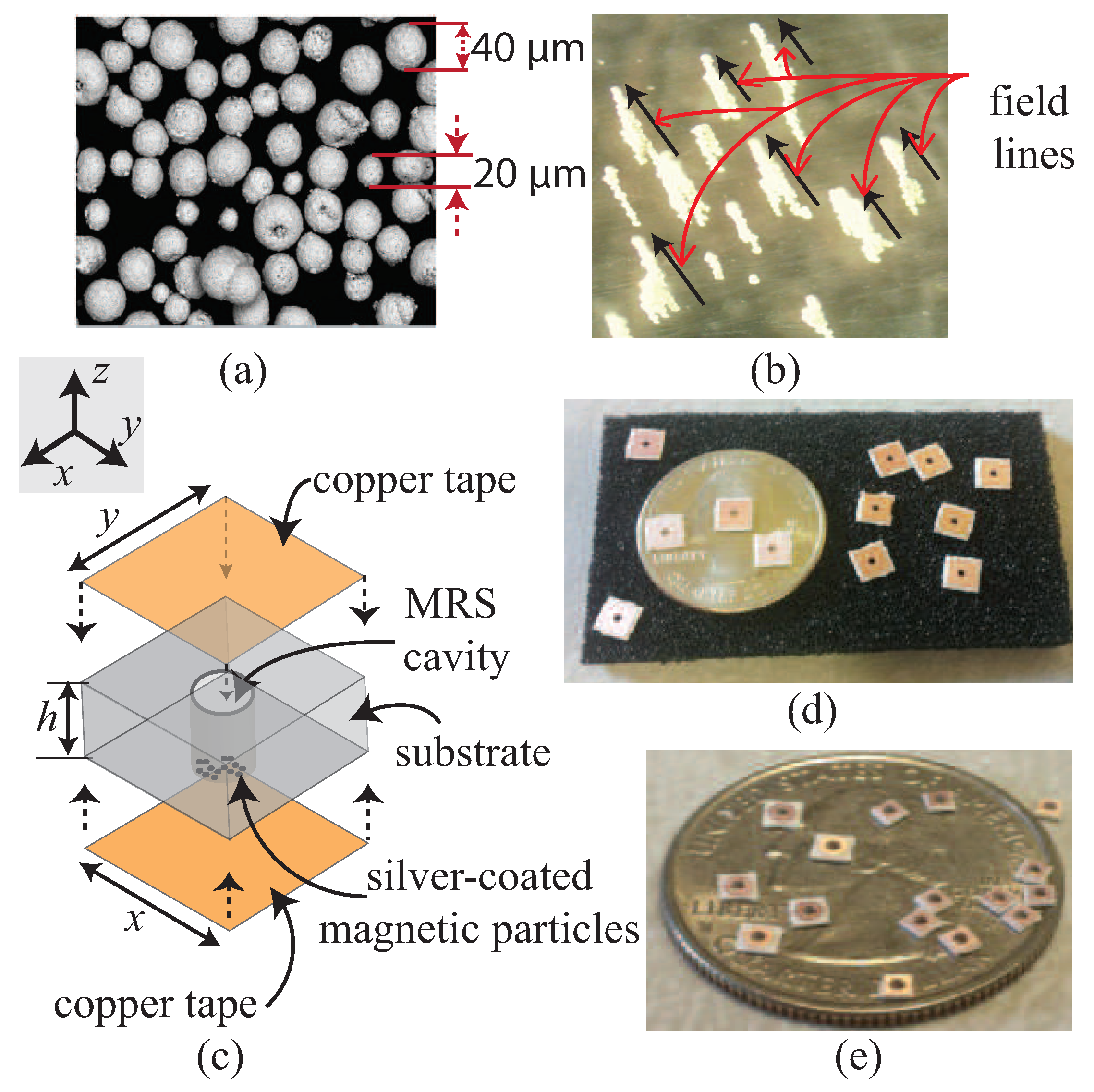
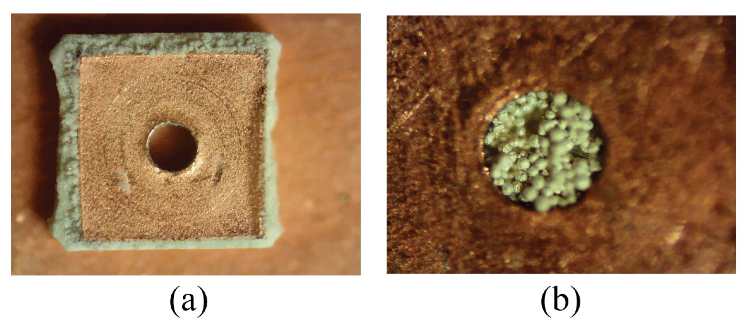
The objective of this paper is to present detailed insertion loss and isolation characteristics of the Magnetostatic Responsive Structures (MRSs), shown in
Figure 1, using ABCD parameters from the measured S-parameters and equivalent lumped element model. The magnetic particles were manufactured by Potters Industries LLC [
7] and a microscopic view is shown in
Figure 1a. The substrate used for the demonstration of the MRSs was Rogers TMM4 [
8]. The behavior of the micron-size magnetic particles in the presence of a static magnetic field is shown in
Figure 1b, whereas the parameters and architecture of the MRSs are shown in
Figure 1c. Two different sizes of MRSs, as shown in
Figure 1d,e, with a cavity diameter of 0.9 mm were filled with the calculated amount of the micron-size magnetic particles having an average diameter of 20
m–40
m. The comparison of the insertion loss and isolation characteristics showed that both MRSs have RF switching capabilities and the smaller the MRSs provided functionality from 100 kHz to 3.5 GHz, when a static magnetic field was applied and removed, respectively.
The novel MRSs have recently been used to frequency reconfigure a printed dipole antenna [
9] and also to achieve a reconfigurable band-stop filter [
10]. In addition, the comparison between the MRSs and PIN diodes used for the frequency reconfiguration of a microstrip patch antenna in [
11] revealed that avoidance of DC biasing circuitry for the MRSs increased the overall antenna performance. Moreover, the bandwidth exploration, signal integrity, benefits of remote biasing, and scalability issues of MRSs have also been reported in [
12]. The applications of the Magnetostatic Responsive Structures (MRSs) [
9,
10,
11] and signal integrity aspects [
12] demonstrated that MRS is a potential alternative switching technology. However, a significant addition to RF switching technology and replacement of the conventional RF switches (PIN diodes, Reed switches, etc.) at low frequencies from 100 kHz to 3.5 GHz and even for higher frequencies could only be possible after complete realization and characterization of MRSs.
2. Development of Magnetostatic Responsive Structures (MRS)
The manufacturing of the MRS was achieved in-house using the LPKF ProtoMat S63 PCB [
13] milling machine. In particular, milling practices were used to make the cavities in a substrate and for accurate cutting of the MRSs. Initially, a 0.9 mm cavity diameter
d on a 3.0 mm × 3.0 mm substrate having a thickness of 0.508 mm
h was accurately manufactured and is shown in
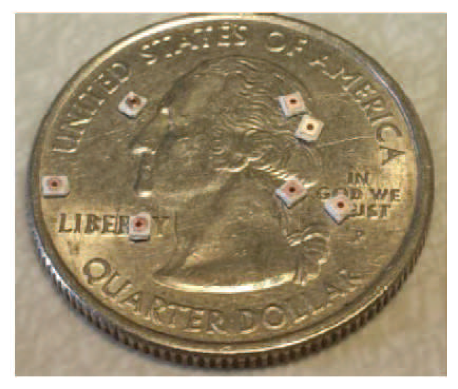
Figure 1d. The substrate material used was a Rogers TMM4 with 1 oz. copper cladding on both the top and bottom. This practice validated the feasibility of milling practices and even smaller structures were manufactured using this milling machine process.
Figure 1e shows the manufactured MRSs cavities with a diameter of 0.9 mm on a Rogers TMM4 substrate having a size of 1.5 mm × 1.5 mm × 0.508 mm.
After the manufacturing of the MRSs, the cavities of the MRSs were then filled with the calculated amount of micron-sized silver coated magnetic particles. The amount of the micron-sized particles was estimated using the Kepler’s problem [
14] for packing of the spherical balls in a cylindrical volume. The derived formula is given as:
where
r is the radius of cylindrical drilled cavity,
h is the height of the substrate, and
R is the average radius of the silver coated magnetic particles.
Equation (
1) was first used to estimate the amount of the silver coated magnetic particles in the cavity having a size smaller than the manufactured MRSs shown in
Figure 1d,e. The smaller manufactured cavities were called a measuring cup and have dimensions of 1 mm × 1 mm × 0.508 mm and
d = 0.4 mm size. The manufactured measuring cup is shown in
Figure 2. This measuring cup was first fully filled with the magnetic particles and the amount of magnetic particles was estimated using Equation (
1). A microscopic view of the measuring cup filled with micron-sized silver coated magnetic particles is shown in
Figure 3. Then, the particles in the measuring cup were transferred to the MRSs cavities by first transferring to a sheet of paper and then migrated to cavities using a static magnet under the manufactured MRSs.
3. Characterization of Magnetostatic Responsive Structures (MRSs) Using ABCD Parameters
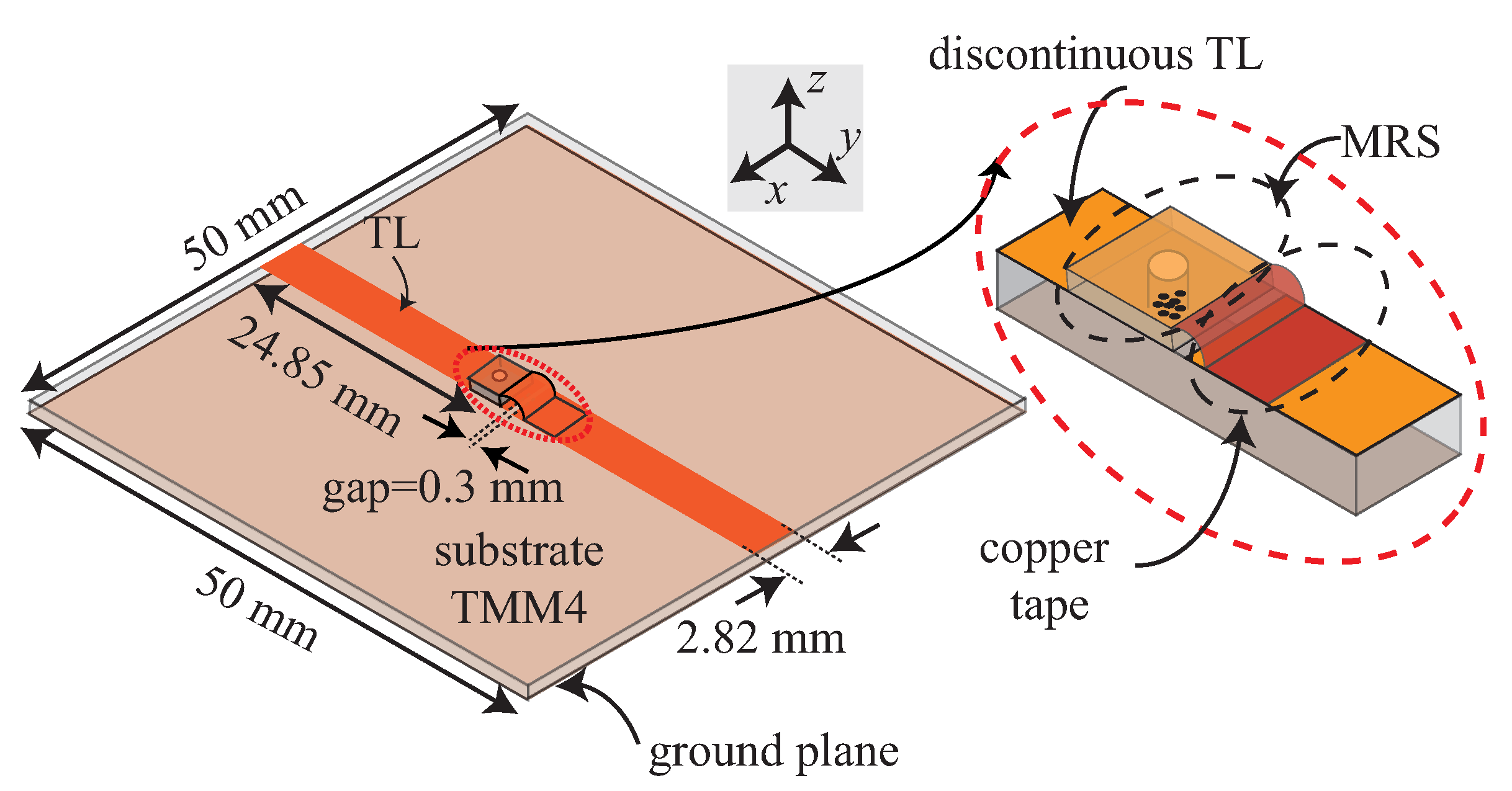
Next, the insertion loss and isolation of the MRSs were extracted using the ABCD parameters by designing and prototyping a discontinuous 50
transmission line (TL) with a gap of 0.3 mm, having dimensions of 50 mm × 50 mm on a 1.52 mm thick Roger’s TMM4 substrate. In addition, 50 mm × 50 mm dimensions of the substrate and length of 50 mm for TL were selected to ensure the EM wave propagation over the frequency of interest and to compare the size of proposed switches with respect to the discontinuous TL, whereas the width of the TL was calculated using standard impedance matching formulas to match with a 50
SMA connector. The dimensions of the fabricated discontinuous TL are shown in
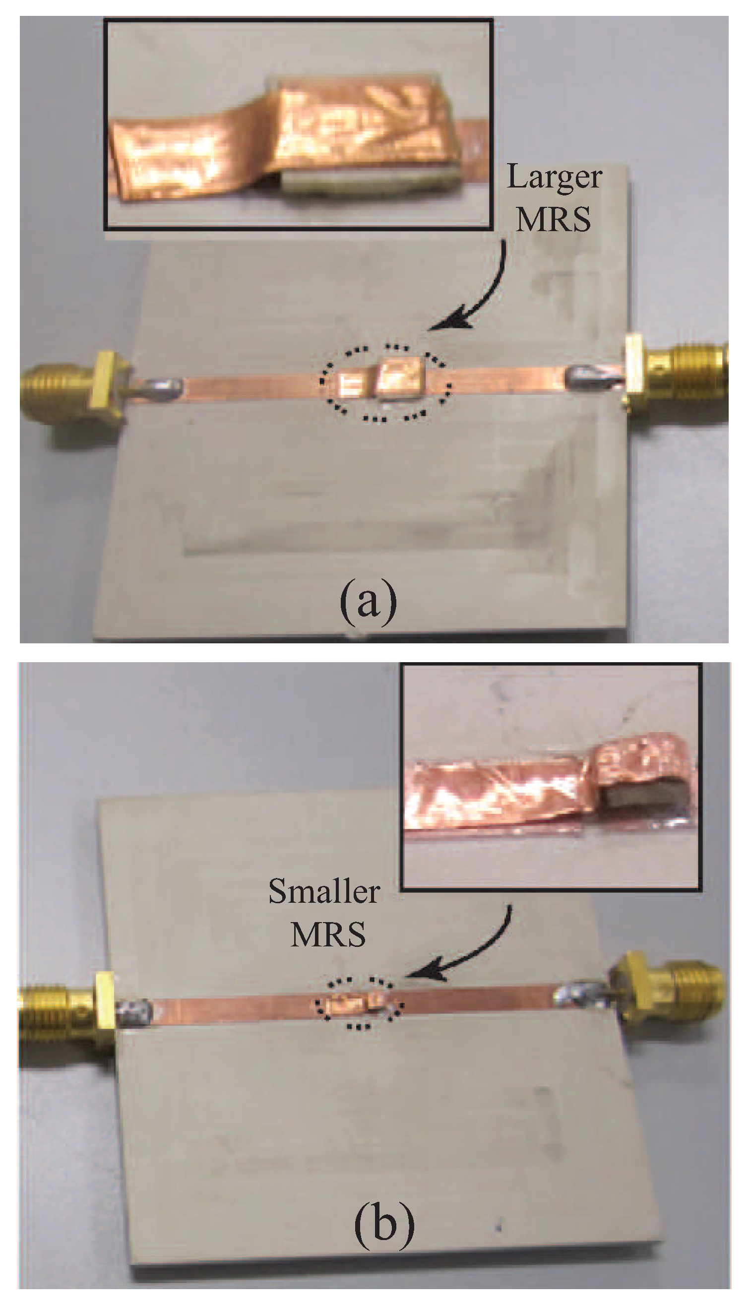
Figure 4. The manufactured MRSs shown in
Figure 1d,e were placed on one side of the discontinuous TL. The top side of the MRSs was connected to the other TL using copper tape, as shown in the expanded view in
Figure 4. The attached MRSs cavities were filled with an estimated amount of silver coated magnetic particles using the measuring cup procedure explained above. After filling the cavities with the magnetic particles, the top of the MRSs was covered with copper foil and the copper tape was used to connect the top layer with the other end of the discontinuous TL. The photographs of the fabricated discontinuous 50
transmission lines (TLs) with the MRSs attached along with the copper tape connection are shown in
Figure 5.
The S-parameters, S
(magnitude and phase), of the manufactured prototype shown in
Figure 5a,b were measured using a calibrated network analyzer E5071C in the absence and presence of a magnetic field. A TRL calibration was also performed prior to the measurements to avoid any inaccuracies. Mathematically,
These measured S-parameters were then converted into ABCD parameters using standard conversion formulas [
15]. For a 50
TL matched with 50
load (
) and source (
) impedances (model shown in
Figure 5), the conversion formulas are:
where
denotes the complex conjugate. Equations (3)–(6) are used to convert measured S-parameters into ABCD parameters and then arranged in a matrix form as:
In a separate experiment, two half 50
transmission lines (TLs) having a length of 24.85 mm (
@ 3.5 GHz) each were also manufactured and the S-parameters, S
and S
of the half TLs were measured and converted into ABCD
and ABCD
parameters using Equations (3) to (6), respectively. After the extraction of ABCD parameters, the ABCD property was used to extract the ABCD parameters of the MRSs in the presence and absence of a magnetic field, as shown in:
and
After the computation of ABCD
, the insertion loss of the MRSs in the presence of the magnetic field and isolation of the MRSs in the absence of the magnetic field were computed using the standard conversions formulas from ABCD to S-parameters [
15]. Finally, the |S
| (dB) values were extracted from the ABCD
parameters to observe the insertion losses and isolation performances of the MRSs.
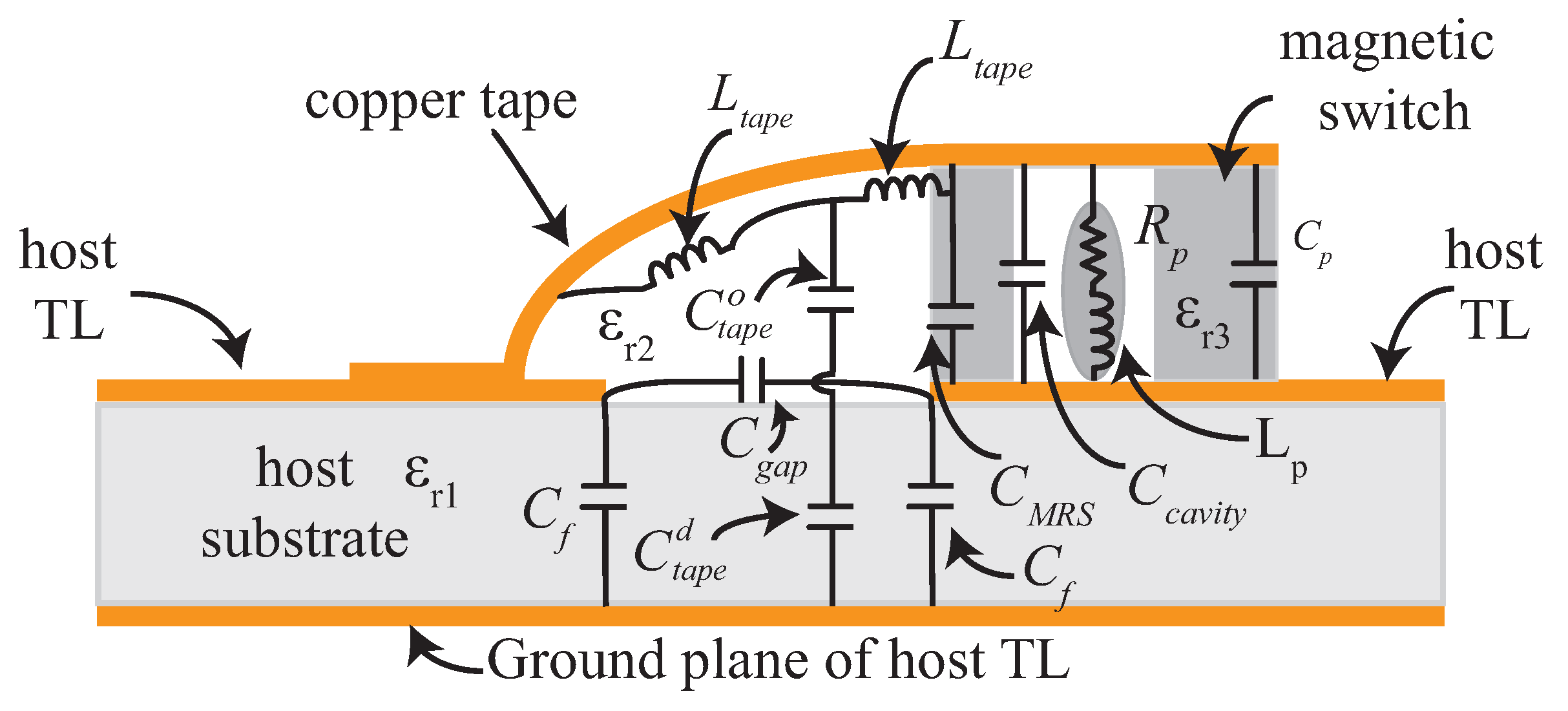
4. Characterization of the Magnetostatic Responsive Structures (MRSs) Using an Equivalent Circuit Model
Next, an equivalent lumped element model of the MRSs was extracted using transmission line theory and microstrip discontinuity theory for a better understanding of the RF switching mechanism and characterization of the MRSs in the absence and presence of a magnetic field. A side view of the MRS and copper tape along with the proposed equivalent lumped element model on a host 50
TL is shown in
Figure 6. The gap discontinuity between the two open ended transmission lines was modeled using the gap discontinuity theory [
16]. The capacitance
was introduced due to the fringing effect of the open ends of the TL and a slight extension of the electric fields without stopping abruptly, whereas the coupling capacitance of the gap was modeled as
. The values of coupling capacitance (
) and fringing capacitance (
) were calculated using formulas given in [
12,
17]. Since the bottom of the MRSs was attached to the one end of the discontinuous TL and the top surface of the MRSs was connected using copper tape to the other half of the discontinuous 50
TL, the copper tape was considered as a suspended microstrip line of finite length over the air and the host TL substrate (TMM4). Thus, the suspended portion of the copper tape was modeled as a series inductance,
along with the capacitances;
and
. The capacitances were attributed to the suspended portion of tape over air and dielectric.
represents capacitance due to the air, whereas capacitance due to dielectric is represented by
. These values were calculated using the following [
16]:
and
when
. For
, equations for C
and C
will be
where
is the relative permittivity of the substrate,
W is the width of the transmission line (which is the same as that of copper tape), and
h is the height of the substrate and air gap between the suspended copper tape and ground plane.
Moreover, shunt capacitances
were accounted for because of the embodiment of the structure, whereas
resulted from the cavity between the top and bottom copper tape. In addition, the capacitance
accounted for the effect of the open-end fringing capacitance of the open-end TL and calculated using the closed form expressions given in [
12,
16]. The values of
, and
were estimated using Equations (7) and (8), whereas
and
were calculated using the formula for parallel plate capacitance [
15]:
Furthermore, the resistance of the magnetic particles was added in the proposed equivalent circuit model of the MRSs to encounter the absence and presence of the static magnetic field. The value of the was made very high because of the air gap in the cavity between and the top copper tape and bottom conductor, as silver coated magnetic particles settled on the bottom surface in the absence of the magnetic field. However, a smaller value of was chosen when a magnetic field was applied to the MRSs.
On the other hand, the presence of the magnetic field aligned the magnetic particles and provided a current path between the top and bottom conductors [
17,
18]. Since the quantity of the magnetic particles was estimated using the measuring cup procedure and Equation (
1), the minimum number of magnetic particles per column
were estimated using the following formula:
where
h is the substrate height of the MRSs and
d is the diameter of the magnetic particles. Then, the total number of columns
in the MRS cavity was estimated using:
where
is the total number of magnetic particles in a cavity and
is the minimum number of magnetic particles per column. It was concluded that, in the presence of the magnetic field, silver coated magnetic particles built
columns with
paths between the top copper and bottom conductor. These paths were considered as a conducting via of
columns having a radius of
× average diameter of magnetic particles, i.e., 40
m. Therefore, the inductance of the conducting via was modeled as
and extracted using the theory of microstrip vias [
18]. The formula used for estimating the inductance of via
formed by columns of magnetic particles in the MRS cavity was:
where
r is the average radius of the via formed by the magnetic particle columns present in the MRS cavity and
h is the height of the MRS substrate.
In the absence of the magnetic field, the magnetic particle did not build up columns in the MRSs cavity, but there were still magnetic particles settled down in the bottom conductor. Thus, for the absence of the magnetic field, the radius
r and height
h in Equation (
16) are equal to the radius of the measuring cup used to fill the MRSs cavity. A complete proposed equivalent lumped element model of the MRSs is shown in
Figure 6.
5. Results and Discussion
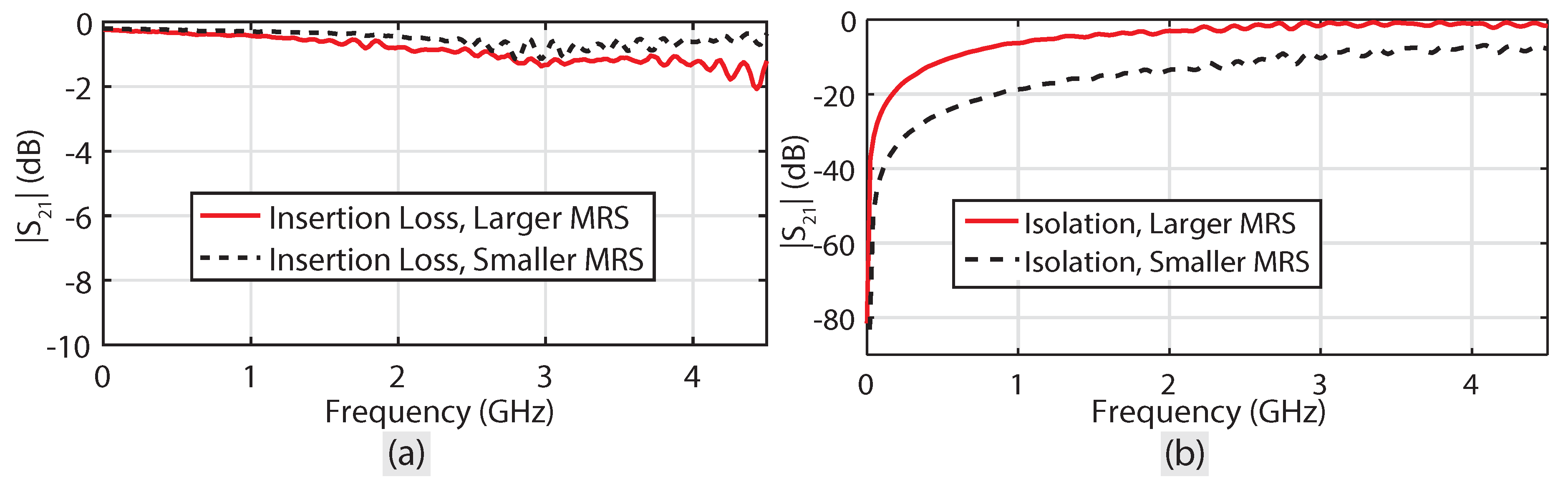
The insertion loss of the smaller and larger MRSs shown in
Figure 1d,e, respectively, were extracted using the ABCD parameters method and procedure shown in Equations (
2)–(
9). The insertion loss and isolation characteristics of both the MRSs are shown in
Figure 7. It can be seen from
Figure 7a that both of the MRSs have an insertion loss (dB(|S
|)) less than 1.5 dB in the presence of the magnetic field i.e., in the ‘ON’ state. However, the smaller MRS has a lower insertion loss, but the general behavior of the insertion loss was the same for both the MRSs. At lower frequencies, the insertion loss was less than 0.5 dB, whereas the insertion loss up to 1.5 dB was observed for higher frequencies. Overall, both the MRSs showed good insertion loss, and it was concluded that the novel structures have a capability to propagate an EM wave over the range of frequencies from 100 kHz–3.5 GHz in the ‘ON’ state.
The isolation characteristics of the MRSs in the absence of the static magnetic field i.e., in ‘OFF’ state were also extracted using the ABCD parameters method and are depicted in
Figure 7b. It was observed that an isolation of 10 dB up to several 100 MHz for the larger MRS was achieved, whereas better isolation performance up to 3.5 GHz was observed in the smaller MRS. The S-parameters extraction of the MRSs from the ABCD parameters and conversion into insertion and isolation performance showed that these novel structures have the potential to be used in RF switching over the frequency range from 100 kHz to 3.5 GHz.
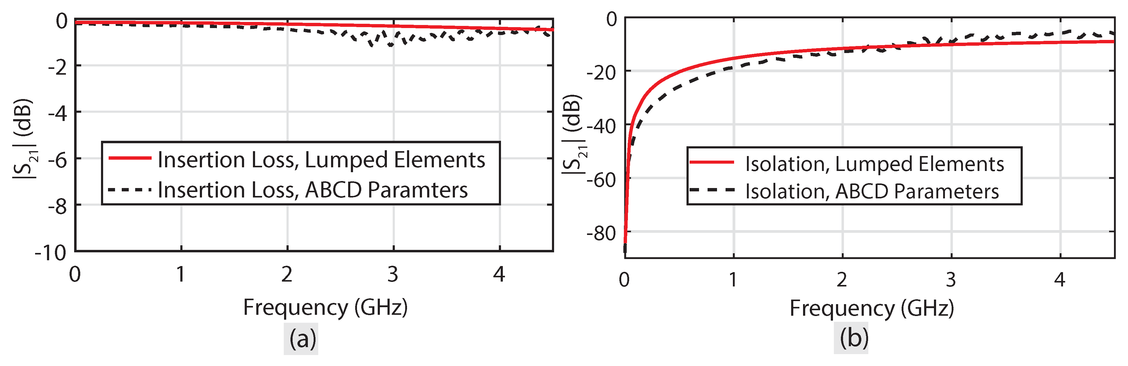
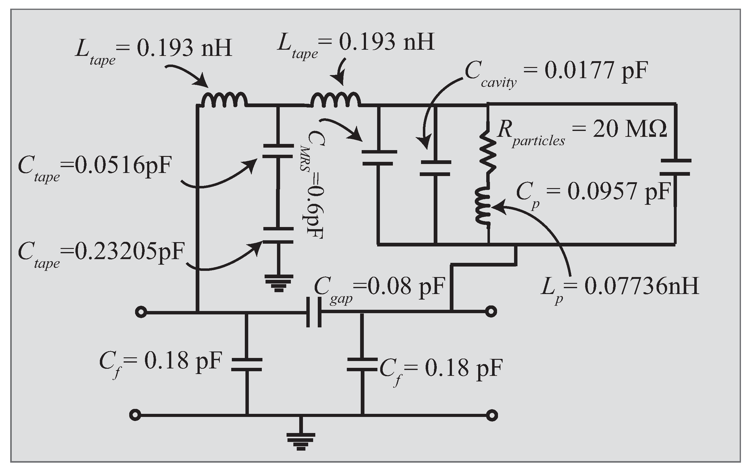
Next, for the validation of the MRSs’ characterization results from ABCD parameters, the values of the proposed equivalent lumped element circuit shown in
Figure 6 for the smaller MRS were extracted using the equations and lumped elements theory discussed in
Section 4.
Figure 8 shows the extracted values of the lumped elements for the smaller MRS in the absence of the static magnetic field, whereas all the extracted values remained unchanged except for the
= 0.2
and
in the presence of a magnetic field.
The circuit shown in
Figure 8 was simulated in Keysight Advanced Design Software (ADS) v. 15.0 [
19] to observe the insertion loss and isolation performance of the smaller MRSs. In simulations, the presence and absence of the magnetic field were mimicked by changing the values of
and
. A comparison between the insertion loss and isolation extracted from the circuit model and ABCD parameters method is shown in
Figure 9. It was observed that the insertion loss of the MRSs was less than 1.5 dB over a frequency range from 100 kHz to 3.5 GHz, whereas an isolation up to 10 dB was achieved. The results comparison of the insertion and isolation values from the ABCD parameters validated the equivalent circuit model and vice versa. Moreover, the results comparison in
Figure 9 showed that the values of the equivalent lumped element in
Figure 6 can easily be extracted for any geometry of the MRSs having different dimensions to achieve better insertion and isolation performances at higher frequencies i.e., greater than 3.5 GHz. It can also be observed from
Figure 9b that the isolation results from the equivalent circuit model are in good agreement with the results extracted from the ABCD parameters method.
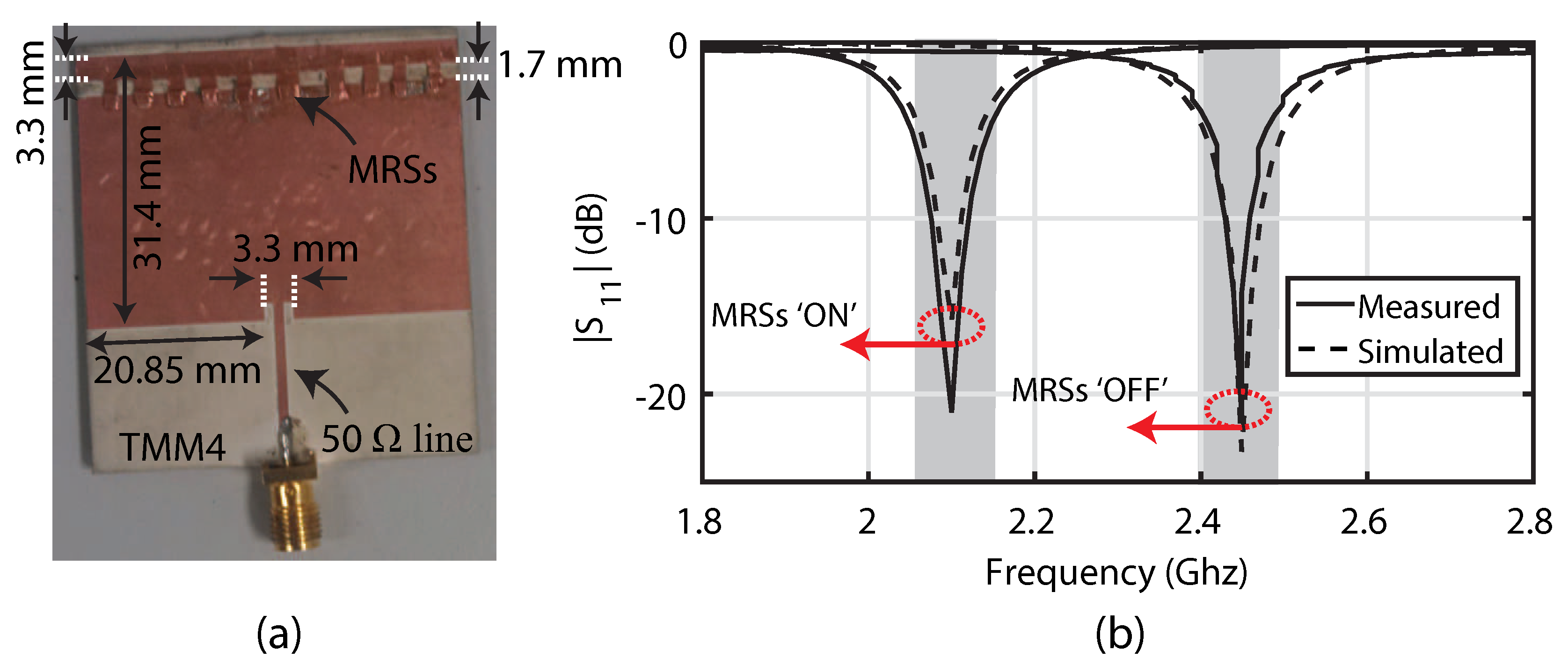
Furthermore, to demonstrate the working of the proposed MRSs as a RF switch, a rectangular microstrip patch antenna is first designed using standard formulas and a small rectangular strip of 3.3 mm width is placed at a distance of 1.7 mm from the rectangular patch [
11]. The small rectangular strip is connected with the main portion of rectangular patch using the proposed smaller MRSs, as shown in
Figure 10a. To mimic the ‘ON’ state of MRSs in simulation, conducting vias connecting the top and bottom that was the main rectangular patch were modelled, whereas, conducting vias were removed in the simulation setup to mimic the ‘OFF’ state of MRSs. On the other hand, during the measurement of magnitude of reflection coefficient (|S
| (dB)), a permanent magnet was used to switch the ‘OFF’ and ‘ON’ state of the MRSs. A comparison of simulation and measurements results is shown in
Figure 10b. It can be observed from
Figure 10b that ‘OFF’ state of the MRSs disconnected the main patch from the small rectangular strip and antenna resonated at 2.42 GHz. On the contrary, ‘ON’ state of the MRSs provided a connection between both the patches and increased overall electrical length of the resonating structure, thereby resulting in a lower resonant band of 2.1 GHz. In total, 10 smaller MRSs were used in the demonstration process to provide a continuous current path between the two conducting patches in ‘ON’ state of the MRSs.
It can be observed from the RF characterization results of the proposed MRSs that these switches can be used in reconfigurable antennas operating from 100 kHz to 3.5 GHz. The proposed RF switches have better insertion loss of −1.5 dB and good isolation performance. However, one may note the high isolation required by reconfigurable antennas. Therefore, increasing the isolation of RF switches beyond −10 dB is the main bottleneck of these switches for high isolation antenna applications. Another limitation of these RF switches can be their operation during rotation along with their possible use in higher band application beyond 3.5 GHz. These limitations can be addressed using symmetric and asymmetric copper files along with the use of thicker embodiment of the RF switches and using multiple holes filled with magnetic particles in the embodiment [
20].
The RF characterization and realization procedure of the novel structures carried out in this work reveal that these structures have a plethora of applications in reconfigurable and tunable antenna design to provide multi-functionality. Another application avenue of the proposed RF switches can be in the fast near-field measurements systems used in microwave imaging with the use of a Modulated Scattering Technique (MST) [
21]. The array of probe antennas loaded with RF PIN diodes can be replaced with the proposed novel switches to measure the near-field distribution over the surface. In addition, the embedment feature of the proposed MRS can be very useful in antennas used for real-time near field measurements with multi-probe technologies under control topology of optimization algorithms and proper switching of MRSs.

 ,
, 
