Article

A One-Cycle Correction Error-Resilient Flip-Flop for Variation-Tolerant Designs on an FPGA

E-SoC Lab/Smart Computing Lab, Department of Computer Engineering, Hallym University, Chuncheon 24252, Korea
*
Author to whom correspondence should be addressed.
Current address: 1 Hallymdaehakgil, Chuncheon, Gangwon, Korea.
Electronics 2020, 9(4), 633; https://doi.org/10.3390/electronics9040633
Submission received: 13 March 2020 / Revised: 27 March 2020 / Accepted: 6 April 2020 / Published: 10 April 2020
(This article belongs to the Section Computer Science & Engineering)

Abstract

:
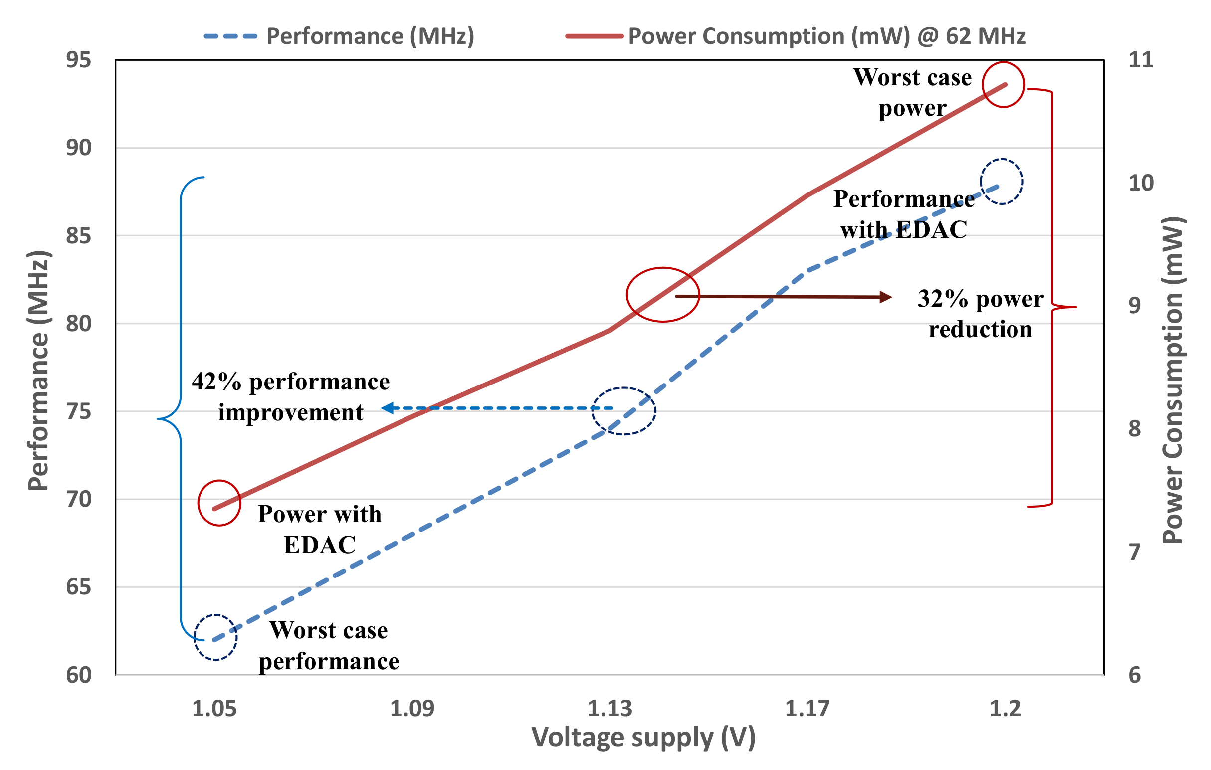
Timing error resilience (TER) is one of the most promising approaches for eliminating design margins that are required due to process, voltage, and temperature (PVT) variations. However, traditional TER circuits have been designed typically on an application-specific integrated circuits (ASIC) where customized circuits and metastability detector designs at a transistor level are possible. On the other hand, it is difficult to implement those designs on a field-programmable gate array (FPGA) due to its predefined LUT structure and irregular wiring. In this paper, we propose an error detection and correction flip-flop (EDACFF) on an FPGA chip, where the metastability issue can be resolved by imposing proper timing constraints on the circuit structures. The proposed EDACFF exploits a transition detector for detecting a timing error along with a data correction latch for correcting the error with one-cycle performance penalty. Our proposed EDACFF is implemented in a 3-bit counter circuit employing a 5-stage pipeline on a Spartan-6 FPGA device (the XFC6SLX45) to verify the functional and timing behavior. The measurement results show that the proposed design obtains 32% less power consumption and 42% higher performance compared to a traditional worst-case design.

1. Introduction

To develop reliable circuits, a traditional synchronous circuit must have a large timing margin to ensure the correct operation under worst-case timing conditions. It means that an appropriate timing margin is added to a clock period to cover the worst-case circuit propagation delays. However, among most of the circuit operation time, the worst-case timing margin is not fully used since the worst-case rarely happens in practice. Therefore, the worst-case timing margin causes higher throughput loss and lower energy efficiency of a design in typical- or best-case conditions.
To minimize the timing margins, many techniques have been proposed for tolerating a timing error that happens in the circuit with the minimal margin. With the help of the techniques, timing margins can be reduced significantly. Generally, the techniques can be categorized into two groups: timing error prediction (TEP), and error detection and correction (EDAC).
TEP circuits [1,2,3,4,5,6] predict a potential error by monitoring data signals. It flags a warning signal whenever the delayed data signals enter an erroneous timing zone that is defined with a clock signal. Then, designer can adjust the supply voltage or clock frequency to ensure correct operation at the edge of predicting a failure. As a result, the output of main flip-flop (FF) always captures the correct data and it does not need any correction. However, in this technique, the timing margin can only be minimized to reserve the enough margin for the correct operation of the main FF. Otherwise, EDAC techniques [7,8,9,10,11,12,13,14,15] detect an actual timing error by monitoring critical paths for late arriving data transitions. Then, it uses extra correction circuits to correct the actually happened error.
In summary, with a timing error resilience technique, we can have the benefits of higher performance and energy efficiency with some minor area overhead thanks to the reduced timing margin when there is no errors with this margin. However, in the case of having more timing errors, the benefits are gradually reduced because of a correction overhead. The term “performance” in our paper is defined as average-case timing performance. The average timing performance is higher than worst-case timing performance since circuits work with the clock frequency optimized for typical operating condition. The worst cases of Process-Voltage-Temperature operation conditions that can induce errors happen rarely.
Generally, most of EDAC circuits are designed in a custom design style and they are implemented in ASIC. They need to optimize their physical designs to satisfy some timing constraint. Moreover, when porting them to a new technology, they cost some efforts for the redesigns on the new technology, leading to the increase of the design times and costs. On the other hand, in an FPGA-based design, it is difficult to implement their designs due to the predefined circuit structures and the un-customized place-and-route (P&R) in FPGAs. For instance, the design of a metastability detector in FPGAs is a critical problem. In addition, the replacement of a traditional FF by a latch in a datapath causes the problem of timing closure in FPGAs. This is because a latch-based design is difficult to meet timing closure with commercial timing tools. Therefore, it is not recommended to replace an FF by a latch in FPGA deigns.
In this paper, for variation-tolerant designs on an FPGA, we propose a metastability-immune error detection and correction flip-flop (EDACFF) working with a one-clock-cycle penalty. The metastability problem can be resolved by imposing a proper timing constraint on a design. Our proposed EDACFF is fully supported by standard cells and it is based on the traditional FF. Therefore, it is suitable with a commercial synthesis tool for an FPGA circuit design. Consequently, it can be ported easily to other process technologies with much less design efforts when compared with other timing error resilience techniques.
The remainder of this paper is organized as follows. In Section 2, we discuss the related works about an EDAC circuit. Next, in Section 3, we propose an EDACFF. In this section, the metastability issue is also considered. Section 4 shows the testing structure for verifying the functional correction of the proposed EDACFF. Section 5 provides the simulation and measurement results from the implementation of the proposed EDACFF on a Spartan-6 FPGA device (XFC6SLX45). Section 6 discusses the presented experimental results and possible future work. Finally, Section 7 concludes the paper.

2. Related Works

In general, traditional EDAC approaches have used ASIC-style implementation. They can be grouped into two categories: (a) FF-based designs and (b) latch-based design.
(a) FF-based Designs [7,8,9,10,11]: Razor in [7] detects an error and recomputes computation to recover the correct results at a reduced clock rate with some minor performance degradation. It includes a main FF, a shadow latch, a multiplexer, and a XOR gate. The XOR gate plays the role of comparing the outputs of the main flip-flop that samples data at a rising clock and the shadow latch that is clocked by the delay clock. Since the output of the main FF can be in a metastable state, the output of XOR gate can be in a metastable state too. Therefore, Razor needs a metastability detector at the output of the FF to guarantee a stable output after the detection for a reliable design.
In [8], a light-weight error detection register using virtual supply rails occupies small area overhead since it requires only eight extra transistors along with a traditional FF. However, Razor-Lite adopts an instruction replay to correct occurred errors and it leads to the high-performance penalty up to 11 clock cycles per correction. In [9], a low-overhead transition detector (TD) with a 9-transistor current sensing circuit is proposed. TDs are inserted at the half-path points of critical paths and TDs predict possible timing errors based on the timing behavior observed at the mid-points of critical paths. So that the timing error in the current clock cycle can be prevented before the real timing violation that can be happened at the endpoint of the critical paths. Thus, it does not need an error correction circuit. However, this design incurs a large area overhead and it needs a significant design effort due to the large number of half-path points of critical paths.
In [10], a timing error tolerant (TET) flip-flop was proposed. It consists of a transition detection unit for an error detection and an FF with preset/clear options for error correction. Whenever an error is detected, the output of the FF is preset to “1” or clear to “0” depending on the input value of the FF. However, this design costs area overhead due to the circuits for generating the preset and clear signals. In particular, this design cannot be implemented in an FPGA since a D-FF structure has only one signal line for presetting or clearing in an FPGA. In [11], an EDAC technique is proposed with a new bit flipping FF. Whenever a timing error is detected, it is corrected by complementing the output of the corresponding FF. However, their design requires a metastability detector to detect the metastability that can be occurred at the output of the FF. Their design is prototyped in a MIPS microprocessor core on an FPGA, but the metastability detector is not implemented in their demonstration.
(b) Latch-based Designs [12,13,14,15]: Razor II [12] is another version of the Razor where a transition detector is used to detect errors. Similar to Razor, it detects timing errors after they actually occur, and it corrects the timing violations using an architectural replay mechanism. A current-based timing error detector was proposed in [13]. It costs a very small area overhead since it requires only 3 additional transistors which are embedded in the FFs that is located on potential critical paths. Bubble Razor in [14] totally replaces the FFs in pipeline stages by the latches. It corrects an error within one clock cycle by sending stall signals to neighboring stages. However, it significantly increases design complexity due to the complex control logic. In [15], a simple error detection latch (EDL) which includes a positive latch and a transition detector is proposed for variation-tolerant designs in ultra-low voltage circuits. Their design has the ability of recovering an error within one clock cycle. However, their design incurs area overhead for padding buffers on short paths.
Surveying through literature, most of the traditional EDAC approaches are designed in a custom design style at a transistor level. Meanwhile, the FPGA chip is a predefined LUT-based fabric and a designer mainly focuses on functional design without considering detailed layouts. It leads to the difficulty of a fine-grain timing control. Moreover, the EDACFF-based design requires a metastable detector which is a component hard to implement in an FPGA. On the other hand, an EDAC latch-based design is not recommended to use in FPGA due to the difficulty of meeting timing violations happen in the latch-based design. Traditional EDAC approaches are not suitable in current FPGAs.

3. Proposed Error Detection and Correction FF

3.1. Error Detection and Correction FF

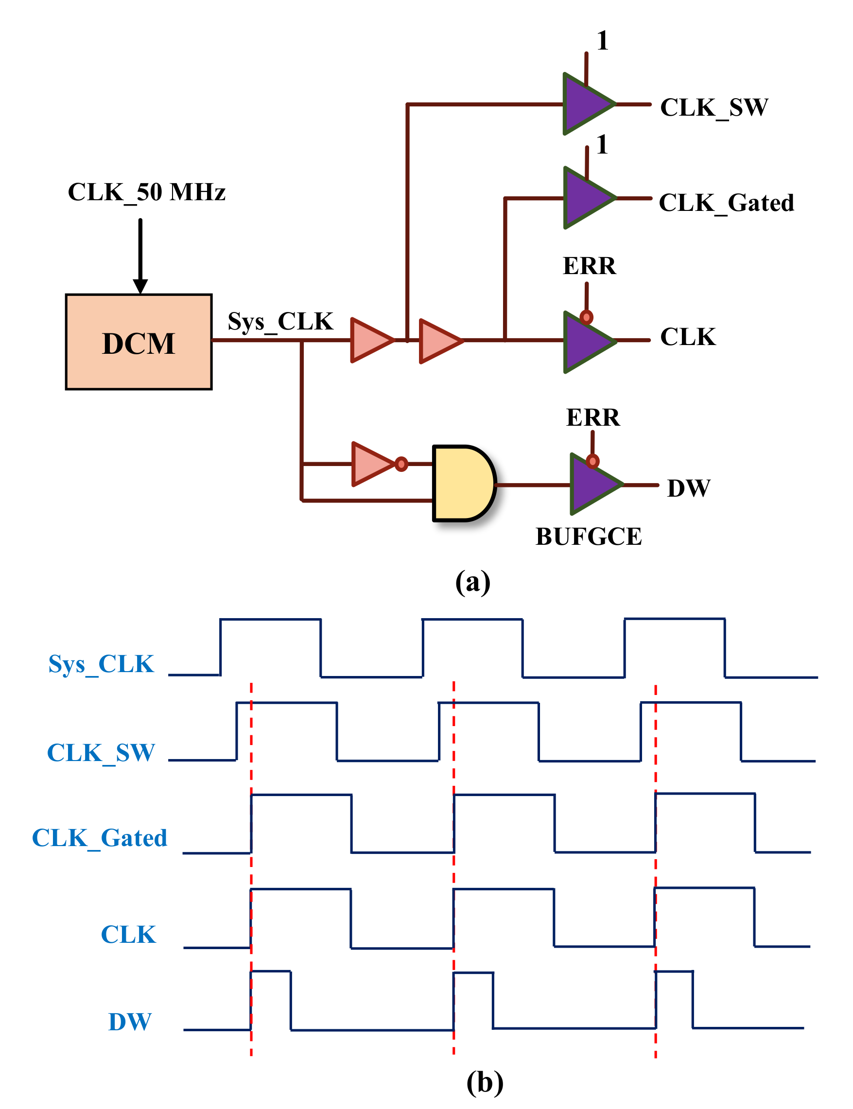
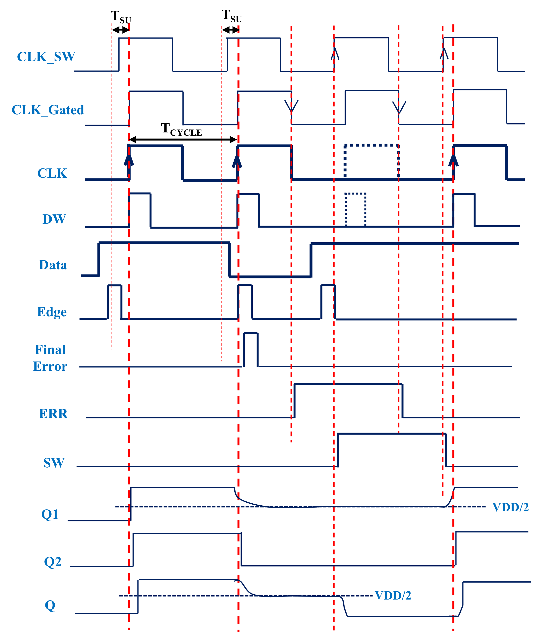
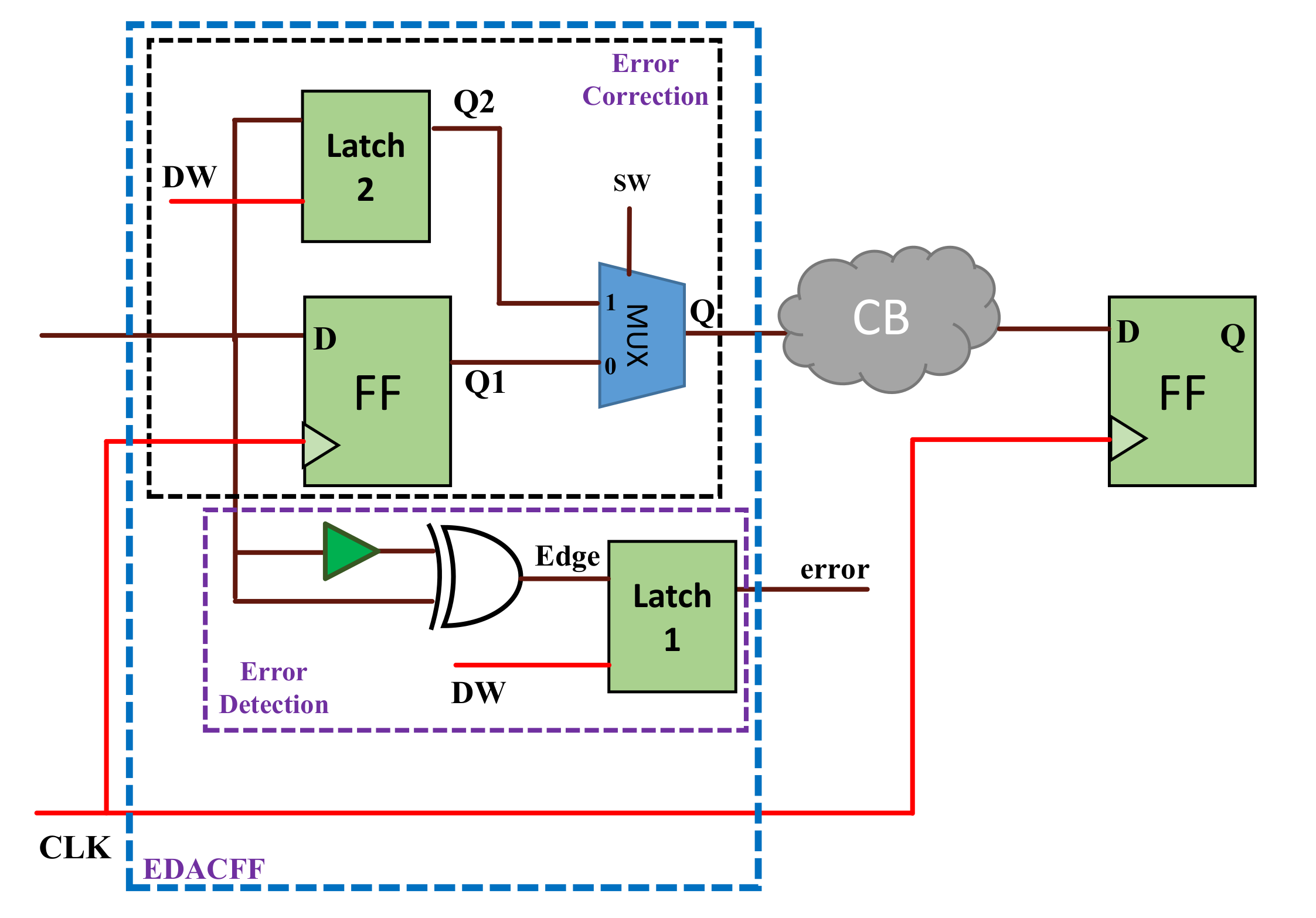
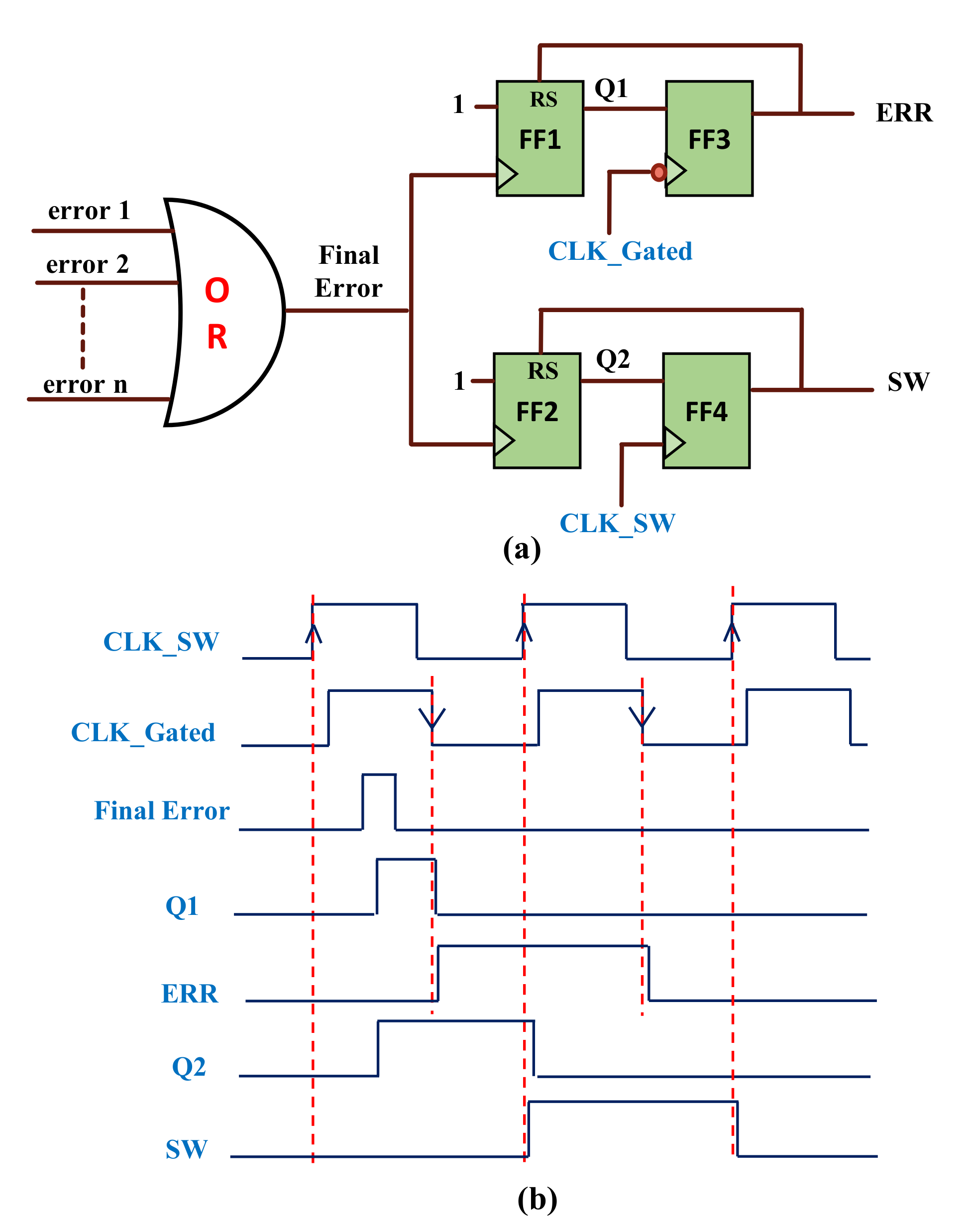
Figure 1 shows the proposed EDACFF which consists of two main parts: error detection (ED) and error correction (EC) circuits. An ED circuit, which is a transition detector, includes a buffer delay, an XOR gate and a latch to generate an error signal whenever a critical path signal transition violates the timing constraints given to a FF. The EC circuit includes a main FF, a latch, and a multiplexer (MUX) as shown in Figure 1. Through the MUX, we can recover the error from the timing violation by selecting a correct value from an FF or a latch. After detecting an error signal, the control circuit in Figure 2 generates the switch signal (SW) for the MUX to select the correct data from the latch 2. This circuit also generates an error pulse (ERR) signal to gate/stop one-cycle clock event to give an enough time margin for error recovery. “CLK_Gated” and “CLK_SW” are clock signals for capturing ERR and SW, respectively. Please note that the ERR signal is captured at the falling edge of a CLK_Gated (it has same phase with CLK) due to the inverted clock input of the FF3. Then, the ERR is used to block the CLK and DW signals as shown in Figure 3.
Our proposed EDACFF does not require the metastability detector at the output of main FF and this is the difference with the previous works [7,11]. In their designs, the output of the main FF is used as input to the ED circuit and it can cause a metastability at the output of ED circuit when the main FF has a metastability. In our case, initially the MUX bypasses the metastability value, Q1, when timing error happens on the circuits in Figure 1. Then, immediately after the error detection, the MUX selects the data Q2 of the latch 2.
However, still the latch 1 and latch 2 in the figure can introduce a metastability. This problem can be solved without using a metastable detector by imposing some timing constraints on the circuits. In detail description will be given in Section 3.5.

3.2. Control Signal and Clock Generator Circuits

Figure 2 shows the control signal circuit and its timing diagram. All error signals will be merged to generate a final error signal which is used to trigger FF1 and FF2. The FF3 samples the data Q1 at the falling edge of the “CLK_Gated”, and then its output signal, ERR, is also used to reset the FF1. This operation is similar to the case of FF2 and FF4 excepting that the FF4 samples the data Q2 at the rising edge of “CLK_SW”.
Figure 3 shows the clock generator circuit and its timing diagram. It consists of a digital clock manager (DCM), buffer delays, an inverter gate, an AND gate, and BUFGCEs. A DCM uses a feature of a “dynamic frequency synthesis” (DFS) to generate multiple clock frequencies internally. When an ERR signal is high, it blocks the CLK and the detection window (DW) signals. Since the clock gating inserts a logic element in a clock tree, the clock gating with normal logic gates is not recommended due to the additional skew and the difficulty in generating a glitch-free signal. For clock gating in FPGA, we must use the recommended dedicated clock control resource in an FPGA. In a Xilinx FPGA, a BUFGCE primitive can be used as a dedicated clock gating logic [16]. This primitive is a global clock buffer with a control input, and it is designed in a glitch-free clock [17].

3.3. Operation of The Proposed EDACFF

The operation of the proposed EDACFF is illustrated in Figure 4. When the data signals arrives before the setup time of FF safely, an Edge signal falls outside of the DW and no error signal occurs (Please note that the “Edge” signal is the output of the XOR gate in the ED circuit shown in Figure 1). On the other hand, when the data arrives late due to some PVT variation and it causes a setup time violation, the Edge signal falls inside the DW and the “Final Error” signal is asserted to high. Then, ERR goes high to stall the next clock cycle, CLK, as well as DW for the time duration that is equal to a single clock cycle. This is necessary since we need to give an enough timing in order to recover a correct logic value. As a result, our design costs only one cycle stall penalty for a detected timing error. Meanwhile, the SW signal also goes high to choose the correct data Q2 of the latch 2 since the data Q1 of FF can be wrong or in a metastable state. Finally, after gating one clock cycle for the error correction, the FF which is in the following stage captures the correct data and the pipeline system operates normally.

3.4. Timing Constraints of the Proposed EDACFF

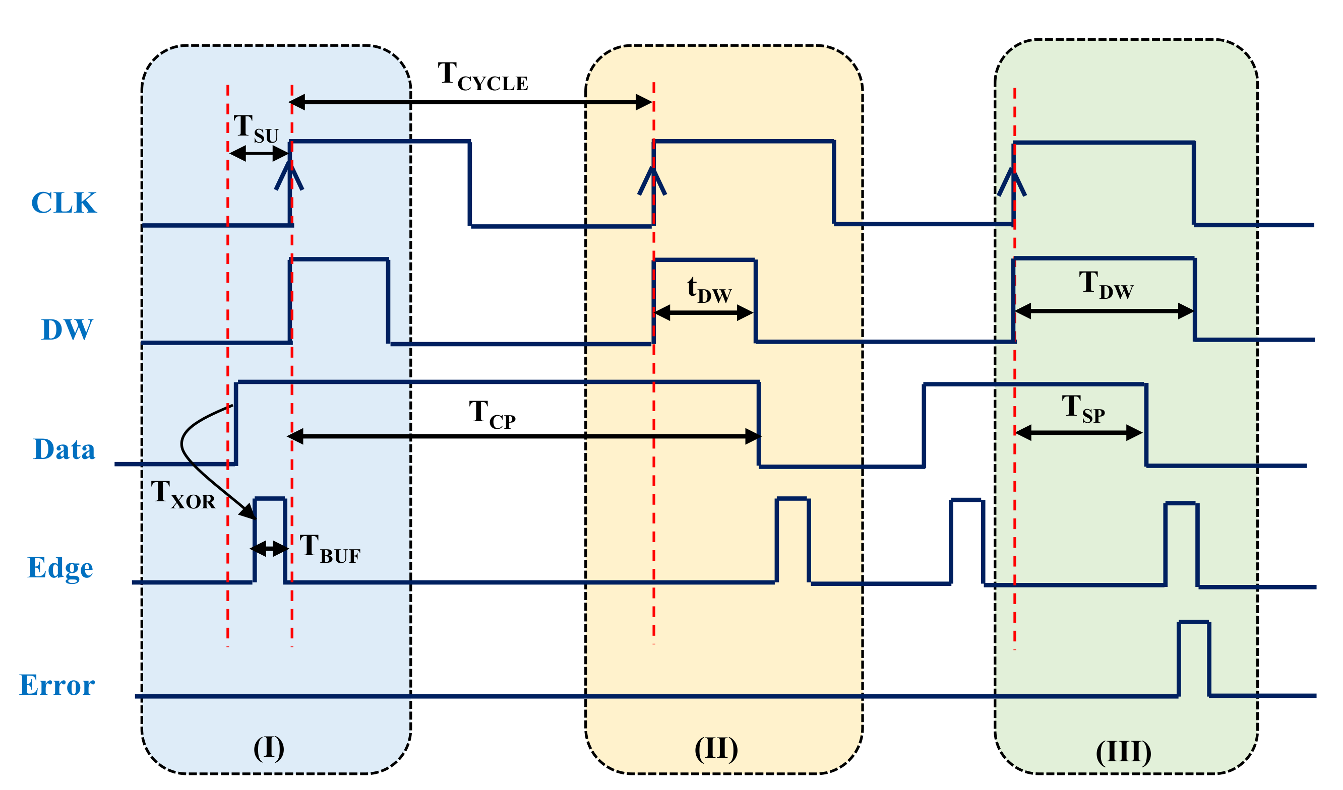
Figure 5 shows the three different cases, I, II and III of having false error detections and each of the cases can be described in detail as follows.
(a) In the case I: if the sum of an XOR gate and a buffer delays is less than the setup time of a FF, the captured data can be in a metastability even an error does not happen. Therefore, in order to guarantee that an error detection circuit generates an error signal correctly, the following timing constraint (1) needs to be satisfied:
T s u < T X O R , B U F
Here T s u and T X O R , B U F are the setup time of an FF and the delays of an XOR gate and a buffer, respectively.
(b) In the case II: if the width of the DW is not large enough to capture an signal arriving at the endpoint of maximum critical path which is slowed down by worst-case PVT variations, the violation will not be captured within the DW. However, the FF samples the wrong data. Hence, the minimum width of the DW must account for the delay variations that cause signal to arrive late. Let t D W is the minimum width of the DW. The following timing constraint (2) needs to be satisfied:
t D W > T C P + T c l k _ q + T X O R , B U F T c y c l e
Here T C P is the maximum critical path delay due to the PVT variations and T c y c l e is a clock period. T c l k _ q is the propagation delay from a rising clock to an FF output. The condition (2) needs to take account of T X O R , B U F delay in order to ensure an edge data still appears inside the DW when the worst-case PVT variations happen.
(c) In the case III: if the width of the DW is larger than the shortest path delay (sometimes, known as contamination delay in digital circuits), it causes the false error detection as shown in Figure 5. Thus, the maximum width of the DW must be smaller than the shortest path delay that causes signal to arrive early. Let T D W and T S P are the maximum width of the DW and the shortest path delay, respectively. The following timing constraint (3) needs to be satisfied:
T D W < T S P + T c l k _ q

3.5. Metastability and Area Overhead Considerations

Our proposed EDACFF can introduce a metastability at the output of Latch 1 and Latch 2 in Figure 1. For the latch-based design where a latch is transparent at a high level, if the timing violation happens during the low to high transition of a DW signal (the latch is opening), the metastability can be resolved quickly just after the data becomes stable. Otherwise, if the timing violation happens during the high to low transition of a DW signal (the latch is closing), the metastability cannot be resolved. Therefore, in order to avoid such a metastability, the minimum width of the DW in condition (2) needs to increase for adding a delay margin which is larger than the hold time of the latch. As a result, the critical path transition always happens safely before the hold time of the latch at the high to low transition of a DW. We must satisfy the timing constraint (4) given as follows:
t D W > T C P + T c l k _ q + T X O R , B U F T c y c l e + T h
Here T h is the hold time of the latch. By satisfying the condition (4), there will be no metastability at the output of latch 1 and latch 2. This is difference with the previous works in [7,11] where metastability in a datapath is resolved by adding a metastable detector.
In Xilinx FPGA devices, a “slice” is a logic resource for deriving functional circuits. It consists of four look-up tables (LUTs) and eight FFs/Latches which share a same clock line. It means that the latch 1 and latch 2 which are enabled by the same DW signal can be placed within a slice. On the other hand, a buffer delay, an XOR gate, and a MUX can be constructed by LUTs. They cost three LUTs. As a result, our proposed design is implemented with only single slice resource.

4. Circuit Structure of Testing EDACFF

Figure 6 shows a block diagram of testing an EDACFF circuit. It consists of three parts: a 5-stage pipeline design (error-free) as a reference, a 5-stage pipeline with EDACFF as our proposed design, and control circuit. The 5-stage reference pipeline employs traditional FFs without combinational circuits between the stages. Therefore, under the PVT variations, all FFs always sample correct values. In the 5-stage pipeline design with EDACFF, a 3-bit counter is used to generate 3-bit input data. The datapaths of the first, the second, and the fourth stages are made as critical paths in the pipeline design.
In Figure 6, CP and NCP mean “critical path” and “non-critical path” circuits, respectively. Since the circuit structure in Figure 6 is for testing the proposed EDACFF, the circuits in CP and NCP are implemented by the dummy functional logics which are constructed by the delay elements. Those delay elements are implemented by cascading multiple look-up table (LUT) resources on an FPGA. Obviously, the number of LUT as delay elements in CP are higher than NCP. Then, EDACFFs are inserted at the endpoint of the critical paths in the first, second and fourth stages.
During the circuit operating time, because of PVT variations, a timing violation may happen and may be detected in EDACFFs. The other stages use traditional FFs. Finally, the value of the last pipeline stage is compared with “always correct value” of the 5-stage reference pipeline. If they are equal to each other, it means that the functionality of the proposed EDACFF is correct, and the error monitoring signal will not be flagged. The control circuit includes the control and clock generator circuits where their operations are explained in detail before in Section 3.2. In our approach, the direct frequency synthesis feature of a DCM is employed in the clock generator circuit to provide a programmable frequency which can be configured with 2 MHz granularity.

5. Experimental Results

The experimental setup for measuring the performance and the power consumption of the proposed design is presented in Figure 7. It consists of an oscilloscope, a DC power supply and a Spartan 6 FPGA board.
Figure 8 shows post-layout simulation results of the design. The “data1”, “data2”, “data3”, “data4” in the waveform viewer are the data values which are captured by EDACFFs and traditional FF at the first, the second, the third, and the four stages of the pipeline, respectively. Please note that the datapaths of the first, the second, and the fourth stages are made as critical paths in the pipeline design. Therefore, EDACFFs are inserted at the endpoint of those critical paths in the first, second and fourth stages. The traditional FF is inserted at the third stage.
When we increase a clock frequency, the clock cycle time is reduced. Therefore, the timing error happens and the EDACFF samples the wrong data (e.g., “data2” samples the wrong value “3” instead of “2”). Hence, the “Final_Error” signal is flagged and then the “ERR_Signal” and the “Switch_Signal” go high to gate/stall one clock cycle for an error recovery. As a result, at the next clock cycle, all FFs sample the correct data as shown in Figure 8. It is noteworthy that an “Error_monitoring” signal keeps low during the whole simulation time. It means that our proposed EDACFF works correctly even though a timing error occurs inside circuits.
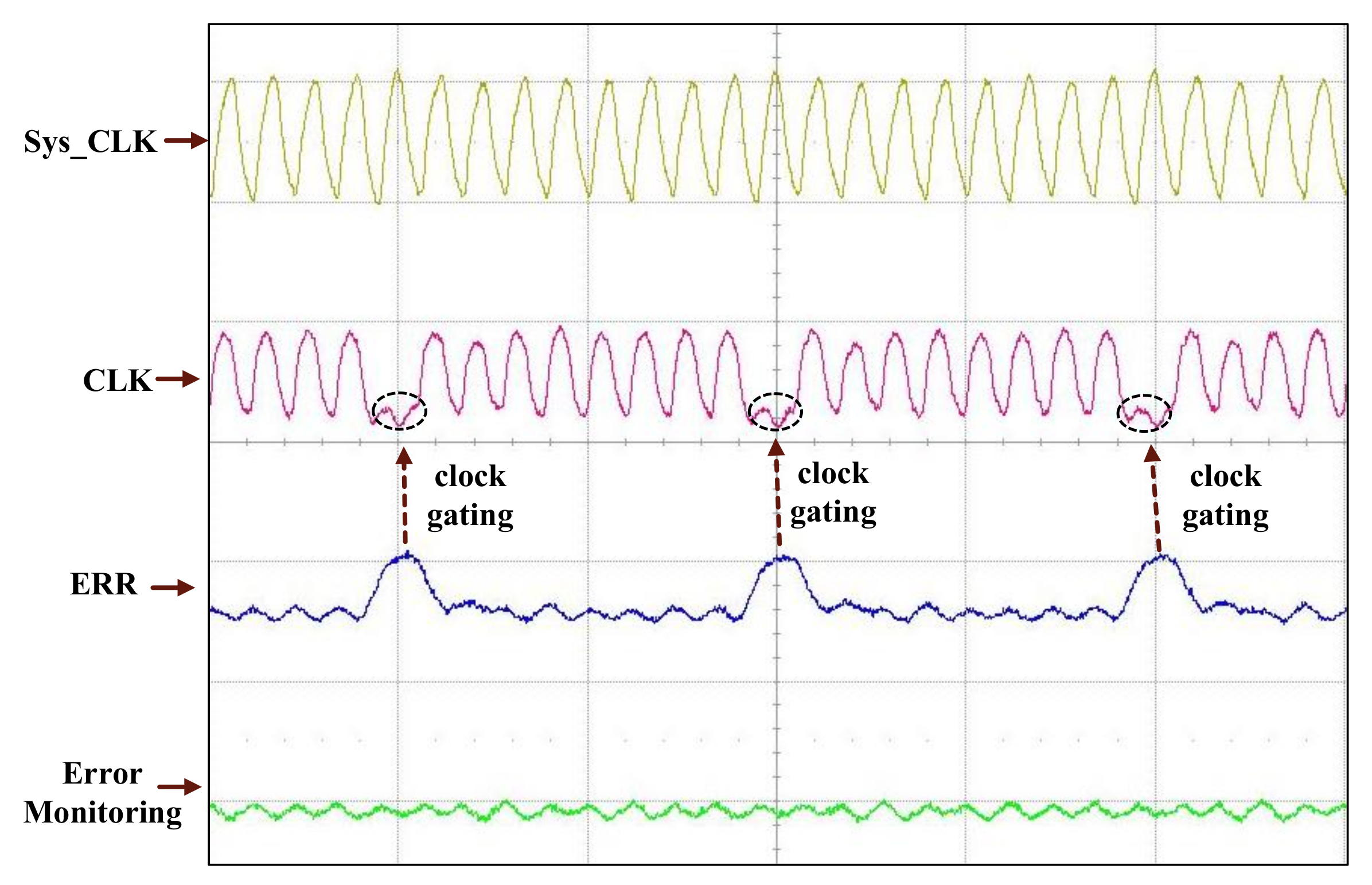
Figure 9 shows the measured signal waveforms of the proposed design. The frequency of the baseline design is 62 MHz at the supply voltage of 1.2 V. Our proposed EDACFF can operate at the point of first failure (PoFF) with working frequency of 90 MHz under the typical operating condition (1.2 V power supply and room temperature). As shown in Figure 9, at the PoFF, the timing error occurs and it causes an ERR signal to go high in order to gate one clock cycle for error correction. Then, the data are sampled correctly at the next clock cycle. In the measurement as well, “Error_Monitoring” signal keeps low and it shows that our proposed EDACFF works correctly in a real situation. Recall that the “Error_Monitoring” signal goes high when the output values of the 5-stage reference pipeline (error-free) and the 5-stage pipeline with our EDACFF are different to each other.
Figure 10 shows the benefit of our proposed design compared with a typical worst-case design. The frequencies of both cases are compared at the same supply voltage of 1.2 V. The power consumptions for the both cases are evaluated and compared at the same frequency of 62 MHz. At 1.2 V, the baseline frequency of the design is 62 MHz (worst-case performance). However, by employing the proposed EDACFF in the pipeline design, our design can work at the clock frequency of 88 MHz (best performance with EDACFF). Therefore, we can obtain 42% performance improvement. On the other hand, we have measured the dynamic power consumption of our proposed design and the worst-case design at the same frequency of 62 MHz. As shown in the right axis in Figure 10, at 1.2 V, the power consumption of the worst-case design is 10.8 mW (9 mA current consumption). On the other hand, our proposed design can operate at a low voltage supply of 1.05 V with 7.35 mW (7 mA current consumption) power consumption at the same performance. Thus, it can save in 32% power consumption.
Table 1 compares our proposed EDACFF with other previous EDAC techniques. The main benefits of our proposed design are that it is fully supported by standard cells and it is based on the traditional FF. Therefore, it is suitable for a commercial FPGA circuit synthesis tool. The row “Design Effort” in Table 1 shows that our design requires less “design effort" compared with other timing error resilience techniques since their works have been designed in a custom design style using a typical ASIC design flow. Moreover, compared with previous works in [8,12], they need more than one clock cycle penalty for a detected timing error. On the other hand, our design consumes only one cycle penalty. The work in [13] also needs one clock cycle for detecting but their design is a latch-based design. A latch is not recommended to use in an FPGA due to the difficulty of meeting timing constraints which should be satisfied in the latch-based design. Both the works in [9,11] consume only one clock cycle penalty. However, the work in [9] needs a metastability detector and the work in [11] incurs a large area overhead due to the large number of half-path points of critical paths.

6. Discussion

Generally, it is hard to directly compare our proposed EDACFF circuit which is implemented on FPGA with other previous EDAC techniques. This is because most of their works have been implemented in ASICs. However, since the previous EDAC circuits [8,9,11,12,13] are designed in a custom design style using an ASIC design flow, their works need much manual circuit optimization. Moreover, when porting them to a new technology, they cost much design efforts for the redesigns on the new technology. This leads to the increase of the design times and costs. Furthermore, the implementation of a metastability detector and using a latch instead of an FF in FPGAs are very difficult due to the timing closure with commercial timing tools. On the other hand, our work focuses on the implementation the timing error resilience technique on an FPGA and we propose suitable architecture of the EDACFF on an FPGA that can be automatically synthesized, placed and routed with commercial computer-aided design (CAD) tools.
The future work will be developing an industrial digital SoC application with the proposed scheme and exploring in-depth and detailed power-performance design space with the real applications. Finally, automatizing such an exploration and optimization could be another possible future work.
7. Conclusions

In this paper, we proposed an error detection and correction flip-flop for variation-tolerant and error-resilient circuit designs on an FPGA. The proposed design occupies only one slice and it can correct an error within a single clock cycle. Moreover, a metastability issue can be resolved by imposing a timing constraint (4) on the circuits. For validating our design, the proposed EDACFF is implemented in a 5-stage pipelined 3-bit counter on a Spartan-6 FPGA device (the XFC6SLX45) and its operational correction is verified by simulations and actual measurements. Furthermore, the measurement results showed that the proposed design consumed 32% less power consumption while achieving 43% of performance improvement compared with a traditional worst-case design.

Author Contributions

Conceptualization, D.M.T. and J.-G.L.; methodology, D.M.T. and J.G.L.; software, D.M.T.; validation, D.M.T.; formal analysis, D.M.T. and N.V.T.; investigation, D.M.T. and N.V.T.; writing–original draft preparation, D.M.T.; writing–review and editing, D.M.T., N.V.T. and J.-G.L.; supervision, J.-G.L.; project administration, J.-G.L.; funding acquisition, J.-G.L. All authors have read and agreed to the published version of the manuscript.

Funding

This work has been supported in part by Basic Science Research Program through the National Research Foundation (Grant numbers 2018R1D1A1B07043399) and Hallym University Research Fund (Grant number HRF-201906-012).

Conflicts of Interest

The authors declare no conflict of interest.

References

  1. Sato, T.; Kunitake, Y. A simple flip-flop circuit for typical case designs for DFM. In Proceedings of the 8th IEEE International Symposium on Quality Electronic Design (ISQED’07), San Jose, CA, USA, 26–28 March 2007; pp. 539–544. [Google Scholar]
  2. Amouri, A.; Tahoori, M. A low-cost sensor for aging and late transitions detection in modern FPGAs. In Proceedings of the Field Programmable Logic, Chania, Greece, 5–7 September 2011; pp. 329–335. [Google Scholar]
  3. Das, B.P.; Onodera, H. Frequency-Independent Warning Detection Sequential for Dynamic Voltage and Frequency Scaling in ASICs. IEEE Trans. VLSI Syst. 2014, 22, 2535–2548. [Google Scholar] [CrossRef] [Green Version]
  4. Valdes-Pena, M.D.; Freijedo, J.F.; Rodríguez, M.J.M.; Rodríguez-Andin, J.J.; Semião, J.; Teixeira, I.M.C.; Teixeira, J.P.C.; Vargas, F. Design and validation of configurable online aging sensors in nanometer-scale FPGAs. IEEE Trans. Nanotechnol. 2011, 12, 508–517. [Google Scholar] [CrossRef]
  5. Ghaderi, Z.; Ebrahimi, M.; Navabi, Z.; Bozorgzadeh, E.; Bagherzadeh, N. SENSIBle: A Highly Scalable SENsor DeSIgn for Path-Based Age Monitoring in FPGAs. IEEE Trans. Comput. 2017, 66, 919–926. [Google Scholar] [CrossRef]
  6. Sannena, G.; Das, B.P. Low Overhead Warning Flip-Flop Based on Charge Sharing for Timing Slack Monitoring. IEEE Trans. VLSI Syst. 2018, 26, 1223–1232. [Google Scholar] [CrossRef]
  7. Ernst, D.; Kim, N.S.; Das, S.; Pant, S.; Rao, R.; Pham, T.; Ziesler, C.; Blaauw, D.; Austin, T.; Flautner, K. Razor: A low-power pipeline based on circuit-level timing speculation. In Proceedings of the 36th Annual IEEE/ACM International Symposium on Microarchitecture, San Diego, CA, USA, 5 December 2003; pp. 7–18. [Google Scholar]
  8. Kwon, I.; Kim, S.; Fick, D.; Kim, M.; Chen, Y.-P.; Sylvester, D. Razor-Lite: A Light-Weight Register for Error Detection by Observing Virtual Supply Rails. IEEE J. Solid-State Circuit 2014, 49, 2054–2066. [Google Scholar] [CrossRef]
  9. Shang, X.; Shan, W.; Shi, L.; Wan, X.; Yang, J. A 0.44V-1.1V 9-Transistor Transition-Detector and Half-Path Error Detection Technique for Low Power Applications. In Proceedings of the IEEE Asian Solid-State Circuits Conference. Seoul, Korea, 6–8 November 2017; pp. 205–208. [Google Scholar]
  10. Valadimas, S.; Arapoyanni, A.; Tsiatouhas, Y. Timing Error Mitigation in Microprocessor Cores. In Proceedings of the IEEE International Conference on Electronics, Circuits and Systems (ICECS), Monte Carlo, Monaco, 11–14 December 2016; pp. 772–775. [Google Scholar]
  11. Valadimas, S.; Arapoyanni, A.; Tsiatouhas, Y. Timing error tolerance in small core designs for SoC applications. IEEE Trans. Comput. 2016, 65, 654–663. [Google Scholar] [CrossRef]
  12. Das, S.; Tokunaga, C.; Pant, S.; Ma, W.-H.; Kalaiselvan, S.; Lai, K.; Bull, D.M.; Blaauw, D.T. RazorII: In situ error detection and correction for PVT and SER tolerance. IEEE J. Solid-State Circuits 2009, 44, 32–48. [Google Scholar]
  13. Zhang, Y.; Khayatzadeh, M.; Yang, K.; Saligane, M.; Pinckney, N.; Pinckney, N.; Alioto, M. iRazor: Current-Based Error Detection and Correction Scheme for PVT Variation in 40-nm ARM Cortex-R4 Processor. IEEE J. Solid-State Circuits 2018, 53, 619–631. [Google Scholar] [CrossRef]
  14. Fojtik, M.; Fick, D.; Kim, Y.; Pinckney, N.; Harris, D.M.; Blaauw, D.; Sylvester, D. Bubble razor: Eliminating timing margins in an ARM cortex-M3 processor in 45 nm CMOS using architecturally independent error detection and correction. IEEE J. Solid-State Circuits 2013, 48, 66–81. [Google Scholar] [CrossRef]
  15. Yu, Y.; Yuan, J.; Xie, L.-L.; Qiao, S.-S.; Hei, Y. A practical, low-overhead, one-cycle correction design method for variation-tolerant digital circuits. IEICE Electron. Express (ELEX) 2018, 15. [Google Scholar] [CrossRef] [Green Version]
  16. Huda, S.; Mallick, M.; Anderson, J.H. Clock gating and clock enable for FPGA power reduction. In Proceedings of the 2012 VIII Southern Conference on Programmable Logic, Prague, Czech Republic, 31 August–2 September 2009. [Google Scholar]
  17. Xilinx Spartan-6 Libraries Guide for HDL Designs, Xilinx, USA, December 2009. Available online: http://www.xilinx.com (accessed on 13 March 2020).
Figure 1. A proposed EDACFF on an FPGA.
Electronics 09 00633 g001
Figure 2. (a) Control signal circuit and (b) its timing diagram.
Electronics 09 00633 g002
Figure 3. (a) Clock generator circuit and (b) its timing diagram.
Electronics 09 00633 g003
Figure 4. Timing behavior of the proposed EDACFF.
Electronics 09 00633 g004
Figure 5. Three cases of having false error detections in the proposed EDACFF.
Electronics 09 00633 g005
Figure 6. Block diagram of testing EDACFF circuit
Electronics 09 00633 g006
Figure 7. Experimental setup.
Electronics 09 00633 g007
Figure 8. Simulated waveforms of the proposed EDACFF design.
Electronics 09 00633 g008
Figure 9. Measured operational waveforms of the proposed EDACFF design at 1.2 V and 90 MHz (POFF).
Electronics 09 00633 g009
Figure 10. Performance and power consumption of the design.
Electronics 09 00633 g010
Table 1. Comparisons with other EDAC techniques.
Proposed2009 [12]2014 [8]2016 [11]2017 [9]2018 [13]
EDAC TypeFlip-FlopLatchFlip-FlopFlip-FlopFlip-FlopLatch
ProcessFPGA (45 nm)130 nm45 nm90 nm40 nm40 nm
Customized designNoYesYesYesYesYes
Design effortLowMediumHighMediumHighHigh
Performance Penalty1 cycle>1 cycle>1 cycle1 cycle1 cycle1 cycle