1. Introduction
Frequency converters (FC) are power electronics that convert alternating current (AC) electrical energy with specified parameters into alternating current electrical energy with desired parameters [
1]. One of the most desirable features of an FC is the generation of output voltage or current with arbitrary amplitude and frequency. In industrial applications, the most common are indirect PC systems with a DC energy storage in the form of an electrolytic capacitor and an output voltage inverter (Voltage Source Inverter (VSI)). Other intermediate FC solutions are systems with a DC storage in the form of a choke and an output current inverter (Current Source Inverter (CSI)) [
1,
2,
3]. FC systems with voltage inverters are widely used in industry, mainly in electric drive [
1,
3], coupling renewable energy sources [
2,
4] and in FACTS systems [
5].
There are several system solutions for voltage inverters, including multi-phase systems as well as different levels of output voltage levels, so-called multilevel inverters [
1]. FC systems with current inverters have not found widespread use in industrial applications. The main problem was the implementation of the current source in the form of a choke as well as its large dimensions and weight. Switching elements used in current inverters were another technical aspect to be solved. The development of the technology of power semiconductor elements in the form of IGBT (insulated gate bipolar transistor) transistors gave new possibilities of using systems with current inverters. At the current state of technology development, several concepts of topological solutions of current inverters were created in prototype laboratory tests [
2,
3,
6].
An alternative to indirect FC is direct FC. The best-known solution for such a system is a direct matrix converter (Matrix Converter (MC)) [
7,
8]. This converter is made of a matrix of bidirectional switches connected between input and output terminals. In addition, a low pass passive filter LC [
9] is used to eliminate higher harmonics of the source current. The basic topology of the direct MC is powered from a voltage source and, in analogy to the indirect FC, it can be called a Voltage Source Matrix Converter (VSMC)—
Figure 1a [
10,
11]. This type of MC configuration has a significant disadvantage in the form of low output voltage gain, which reaches a maximum value of
KU max = 0.866, for undistorted load current [
7,
11]. This property limits or creates severe application restrictions in potential MC applications.
For example, when applying MC in a regulated speed electric drive, it is necessary to use motors with a lower-rated voltage or to use supply voltage boosting systems. Lack of these solutions will result in lowering the motor’s rated torque, which depends on the supply voltage. Similar to the intermediate FC, the matrix converter has several solutions including intermediate topologies (without DC storage) [
7,
11,
12] and multi-level [
13]. The configuration of power electronic switches for direct MC is symmetrical and allows the bi-directional flow of electricity from the power source to the load and from the load to the power source. The load is usually a current source (e.g., induction machine), and the power supply circuit is a voltage source. For this source configuration, MC can also be considered as a system fed from a current source with a voltage source load. The nature of the voltage source load can meet the capacitor of the output voltage filter, and the load can also be an induction machine [
10,
11]. Because the power grid provides us with a stable voltage source, the practical implementation of the current source is a series connection of an alternating AC voltage source with a high inductance choke [
14]. The MC configured in this way is called the Current Source Matrix Converter (CSMC) (
Figure 1b) [
14]. MC fed a current source gives the possibility of increasing the voltage on the load terminals. The disadvantages of this solution are the need to use large input chokes and the dependence of the voltage gain characteristic on the load change [
11].
To distinguish the MC topology, it should be stated that the basic topology of the direct Matrix Converter (MC) is powered from a voltage source and it can be called a Voltage Source Matrix Converter (VSMC). Furthermore, MC can also be considered as a system fed from a current source with a voltage source load, then we call such a converter a CSMC.
The available scientific literature lacks publications presenting detailed CSMC models describing the properties of the system, including the used control strategy. In articles [
14,
15,
16] dealing with CSMC, the authors propose a control strategy that is verified in simulation studies. There is no analysis of the basic properties of the converter showing voltage gain relationships depending on various system parameters (e.g., in the form of static characteristics). In [
17] the authors present the CSMC model but do not present any static characteristics. The presented property analysis is based on the presentation of time waveforms of voltage and current signals. However, the work [
18] presents selected static CSMC characteristics obtained in a fairly complicated and extensive modeling process. The approach presented also does not take into account the control strategy used. In [
19] authors shown only show the operating principle and general characteristics of the converter.
The modeling of CSMC presents significant challenges, due to their discontinuous switching behavior. Furthermore, given the increasing number of different modulation strategies, it is necessary to study their impact on converter properties. In order to achieve their goal, CSMC must be appropriately modeled in simulation or analytical studies. Hence it is necessary to create simple analytical models. There are several approaches to modeling switching converters. Some of them have already been used for MC analysis. The averaged state space method deserves special mention. In this method, only fundamental components of input/output voltages frequency are taking into account without higher harmonic components and power losses which are in the experimental setup. There are few methods for determining the equations of averaged state variables, e.g., the method using the theory of four terminals network [
20], creating flow graphs [
18] or directly creating equations using two-frequency d-q transformation [
21,
22].
In this paper, the average-state space method and the two-frequency d–q transformation are used to model CSMC with tow control strategy Venturini and Space Vector Modulation (SVM). The basics of modeling were taken from the article [
22] and applied to the CSMC topology. The main aim of this paper is to present mathematical models of CSMC for two control strategies and analysis and comparison of static properties of the CSMC system.
2. Current Source Matrix Converter
The schematic diagram of the current PM is shown in
Figure 1b [
14,
15], where the current source input chokes are connected to the input terminals of the switch matrix. Output capacities are connected to the load terminals to determine the nature of the load as a voltage source. Configurations of bidirectional connectors used in all systems presented in the article are presented in
Figure 2. The output voltage waveform is implemented by switching bidirectional switches. These switches implement the appropriate sequence of connections between the output and input terminals in such a way that the current can flows in two directions.
During matrix operation, the switches, regardless of the polarized voltage in the circuit and the direction of the flowing current, are turned off and on at a certain moment. The control function of the switches can be represented as follows [
11]:
for which j ∈ {a, b, c}, k ∈ {A, B, C} where: a, b, c are the phase source terminals, while A, B, C are the output terminals of the CSMC. The switches must be controlled so that there is no short circuit of the output phases and that the current flow is always ensured in each phase of the current source (on input terminals). This is possible if only one switch will be turned on in each source phase of CSMC:
All allowed switch configurations are shown in
Table 1 [
11,
22].
The currents and voltages relationship in the CSMC system are determined by Equations (3) and (4). A 3 × 3 matrix system provides 27 allowed configurations of power electronic switches resulting from the limitation Equation (2). These configurations can be combined into three groups similar to VSMC but the way of connecting the input and output lines is described as follows. The first one includes three zero configurations—all three source phases are connected to the same output phase. The second group consists of active configurations. In this case, two source lines are connected to the same output line. In the third group, one input phase is connected to one output phase. The relationship between the CSMC (
Figure 1b) source-side and load-side currents and voltages is described as follows [
22]:
where
T is the transformation matrix,
- are switch state functions depending on the used modulation strategy.
It should be emphasized that the load current and voltage at the input terminals of matrix switches are shaped in the CSMC, inversely than it is the case in the classic MC. Then we adjust the voltage gain indirectly by adjusting the load current. The input power factor is also indirectly controlled by forcing the source current phase shift by setting the voltage on the input terminals of matrix switches.
3. Venturini Modulation Strategy
The classic Venturini method presented by Venturini and Alesina [
23] consists in modifying the switching state function in the transformation matrix using low-frequency modulation functions. This allows you to specify the intervals for controlling the switches in the converter. The transition (transformation) function is represented by the relationship Equation (5).
where
djK(t) =
tjK/
TPWM pulse duty factor of the state function of the switches
SjK. In publication [
23], Venturini and Alesina proposed the first control strategy based on two modulation matrix
and
. The voltage gain for this control strategy is between 0 and 0.5. It this method is possible to control the input phase shift angle in the range:
. To control the input phase shift angle in the range from 0 to
, then M + is used as follows:
Whereas for controlling the input phase shift angle in the range from
to 0, then M
− is used:
where:
,
, , is the voltage gain: , , and is the pulsation of the supply and load voltage respectively, is the phase shift of current relative to voltage of at source and load terminals of MC.
In this article, only one modulation matrix was used for CSMC control without control of the source current phase shift relative to the source voltage. Then, simplified modulation functions were defined as follows [
24]:
4. Space Vector Modulation of CSMC
The operation of the CSMC converter can also be described using space vector modulation - SVM. In this method, voltages and currents are represented by appropriate space vectors. The basic equation for the presentation of three-phase signals using space vector is defined by Equation (9).
in which:
represent the instantaneous values of three-phase variables, while
is a unitary complex rotation operator. The input voltages and output currents of CSMC can be expressed in its space phasor form as [
22]:
where:
αi are the phase angles of the output voltage vector,
βO are the phase angles of the input current vector.
The allowed switching configuration of the current source matrix converter in the SVM algorithm is shown in
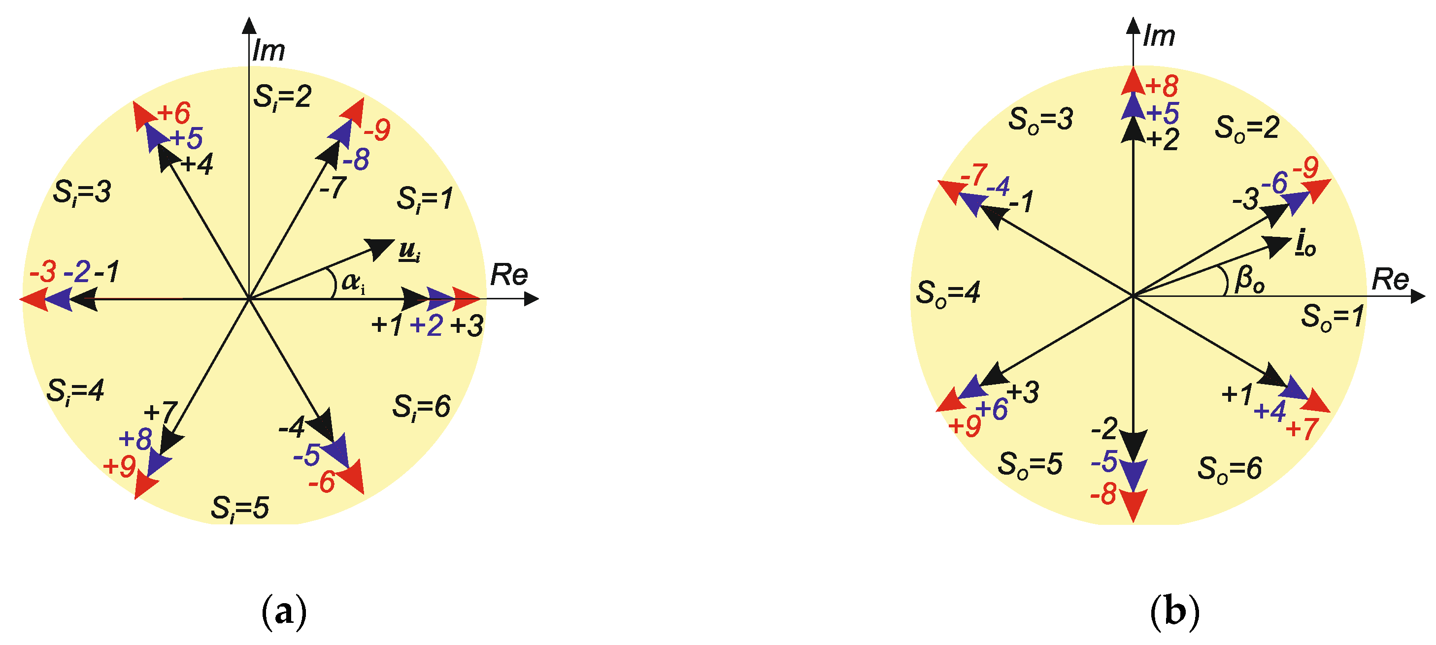
Table 2. Only active and zero configurations are used in this control—a total of 18 allowed configurations. Graphic interpretation 21 configurations of switches are shown in
Figure 3. Active configurations corresponding to non-zero voltage and current vectors have the following designations: (± 1, ± 2, ± 3), (± 4, ± 5, ± 6), and (± 7, ± 8, ± 9). In
Figure 4 the voltage
ui and current
iO vectors for CSMC corresponding to the 18 active configurations are shown. The complex space vector plane is divided into six sectors
Si for source voltages and six sectors
SO for output current. The reference source voltage and load current space-vectors are determined by selecting 4 active configurations (vectors), applied to in a specific sequence and time intervals within the switching sequence period
TSeq—Equations (12) and (13). The zero configurations are applied to complete time interval
TSeq. Modulation duty cycles for switching configuration are defined as follows Equations (14)–(17). The synthesis process of source voltage and output current space-vectors for
Si = 1 and
SO = 1 is presented in
Figure 5.
where
φi is the input phase displacement angle,
and
are the angles of the input voltage and output current vectors measured from the bisecting line of the corresponding sectors, and are limited as follows:
and
.
5. Modeling Theory
The local average of any time-domain function
q(t) is defined by the relationship [
25]:
where
d(t) is the continuous duty cycle. If
, then this determination is true for the next sequence periods. Then
is the duty cycle in the
k-th cycle. The average state-space equation is expressed by the relationship [
26]:
In this equation,
represents the averaged state variable vector,
is the averaged matrix of state variables,
is the averaged input matrix. During operation, the converter assumes different states. These states are subject to analytical combinations on which the averaging method in the space of states is based. Fig. 5 presents the idea of the average state space method related to the Current Source Matrix Converter which topology is presented in
Figure 1b.
CSMC are characterized by the fact that they have 27 possible switching states. The block diagram shown in
Figure 6 allows us to understand the modeling process. It is assumed that the state model is linear for each of the possible switch configurations. Each of these configurations creates a separate model. Then these models are integrated with the help of the averaged
dk duty factor. Each of these configurations can be represented by the Equation:
where:
x - state variable vectors,
- state matrix and
- input matrix for the
k-th configuration of the switches. The general form of the mathematical model based on the average space equations for CSMC is described as follows:
where:
The average space-space model of the CSMC presented in Equation (21) is a time-varying model. Responsible for this is the time-varying pulse duty cycle
. A reduced time-invariant model of the CSMC can be realized by using two-frequency transformation matrix
K described in
d-q rotational coordinate frame:
In these equations, the
is the
d-q transformation matrix for supply voltage pulsations, while the
is the
d-q transformation matrix for load voltage pulsations. To get a stationary equation, substitute the expression:
in Equation (21) assuming that the frequency converter is a symmetrical system. As a result of this substitution, new state variables will appear. So Equation (21) will take the form:
where:
The solution of Equation (26) was described in [
21] and have the following form:
where I is a unit matrix, while
represents the vector of initial values of transformed variables. The values of averaged state variables in steady-state are represented by Equation (30) [
21]:
The relationships Equations (29) and (30) can be used in the study of the operation of the CSMC presented in
Figure 1b for different modulation schemes. This article will present the results of research for the simplified Venturini—described by Equation (8) and SVM—described by Equations (9)–(17).
6. Modelling of CSMC with SVM
The relationship (12) determined the relative switch-on time of the individual switch configuration—corresponding to base vectors, of the output currents and input voltages at the terminals of matrix switches for CSMC with SVM. Subsequent base vectors are turned-on with the following sequence which are defined in
Table 3:
For the order of inclusions so adopted, the transformation matrix D, for example,
Si = 1 and
SO = 1 is determined by the relationship:
Finally, matrix
D has the following form:
By replacing the switching times
d1,
d2,
d3 and
d4 by appropriate formulas defined by dependencies Equations (14)–(17), the matrix
D takes the final form:
When constructing a mathematical model of a matrix converter with space vector modulation, it should take into account the potential difference between a grounded three-phase power point and a zero load point
uNn (
Figure 1b). This voltage is called the unbalance voltage and it its average value is expressed by the relationship:
Taking into account the Equation (3) the unbalance voltage
is given by the formula:
Ultimately, the imbalance voltage takes the form:
where:
Taking into account Equations (9)–(39) yields the final form of the averaged state space model (20) of the CSMC with RL load (
Figure 1b) with space vector modulation is defined by Equation (40). To sum up the presented analysis, we can define the following block diagram presented in
Figure 7, describing the procedure of determining the model of average state-space variables for CSMC with SVM.
8. Validation of CSMC Average Model with SVM and Venturini Modulation
Validation of the obtained models is presented for the following parameters: LS = 10 mH, RLS = 0.1 Ω, CL = 30 μF, RL= 30 Ω, LL = 1 mH. Investigations were carried out on a system consisting of an idealized power stage RSjk=0 in conduction state and RSjk=∞ in the open state.
In
Figure 8,
Figure 9,
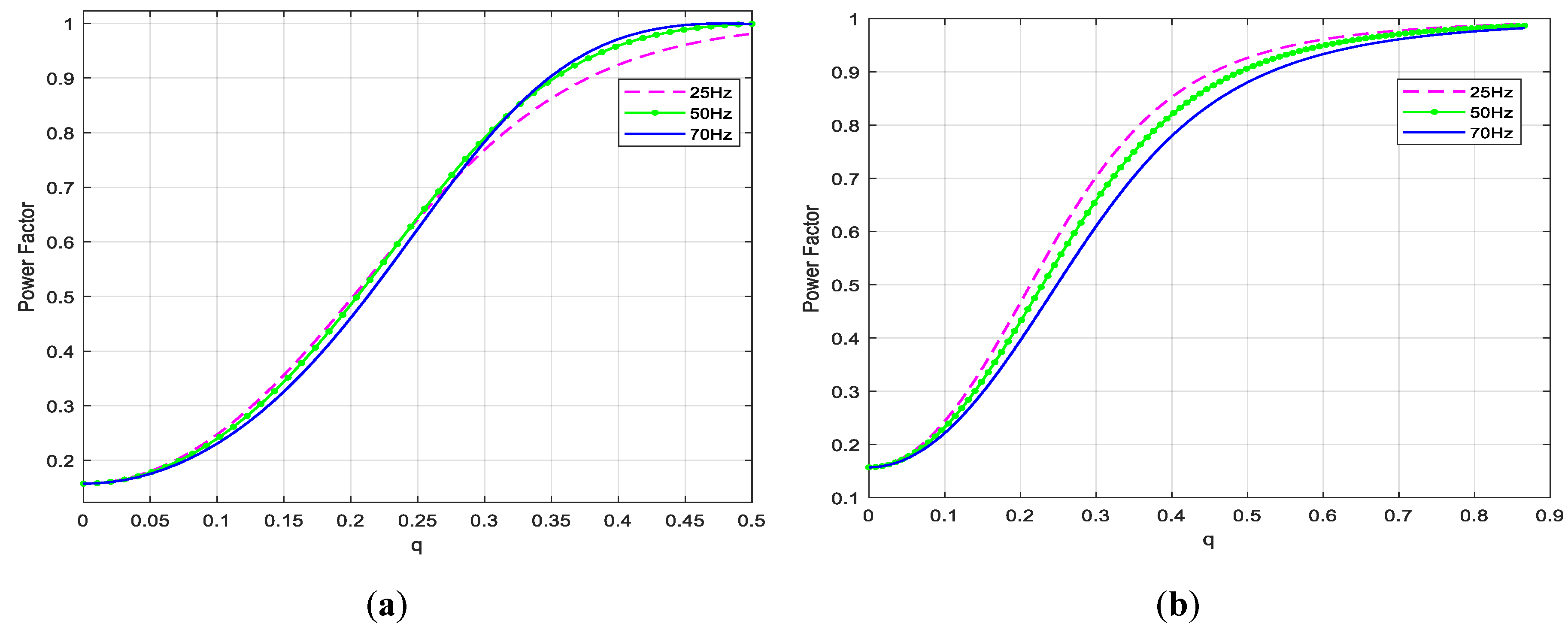
Figure 10 steady-state characteristics of the voltage gain, current gain and input power factor as functions of pulse duty factor
q for Venturini (index (a)) and SVM (index (b)) are shown. As you can see from the presented characteristics, CSMC eliminates the VSMC disadvantage, i.e., reduced voltage at the output terminals. For CSMC, even a voltage gain of about 2.5 times for Venturini type modulation and about 3.5 times for SVM type modulation was obtained. For Venturini modulation, the current transformation characteristic is more linear than for SVM (
Figure 9), while the output power factor is more beneficial for SVM control (
Figure 10). All the presented characteristics from
Figure 8 Figure 9 Figure 10 change slightly depending on the set frequency of the output frequency.
The real power source, built from a serial connection of a voltage source and a high inductance choke that powers the CSMC, changes its parameters depending on the load condition. The characteristics of
Figure 11 show the effect of load resistance changes on voltage gain. Increasing the load (reducing the load resistance) causes a decrease in voltage gain. However, it should be noted that for current source parameters assumed in the article, the value of voltage gain is greater than one for a load resistance of about 20 Ω. With a properly designed control system in a closed control loop, it will be possible to maintain the nominal value of the output voltage, as well as stabilize this voltage in the event of supply voltage sags. The characteristics for SVM control are more linear and for Venturini modulation, there is a decrease in voltage gain for larger values of load resistance. This is due to the phenomenon of resonance occurring between elements of the power source, output filter and load, which is more important when switching on synchronous configurations (each input phase is connected to a different output phase), which occur only in the Venturini method.
Figure 12;
Figure 13 show the characteristics of the current gain and input power factor depending on load changes. It should be noted that there is no significant increase in source current that would result from the phenomenon of increasing the output voltage, as illustrated by the current gain characteristics of
Figure 12. A negative phenomenon is the lack of a unit input power factor (
Figure 13). For SVM control it is possible to regulate it indirectly by forcing the phase shift of source current source by appropriate shaping the voltage on the input terminals of the matrix switches (
ua,
ub,
uc). In the presented results, the phase shift value of the input voltage relative to the source current is set to zero, which does not mean that the source current will be in phase with the source voltage.
In order to investigate the impact of the given output voltage frequency and changes in load value on the voltage gain characteristics, 3D characteristics illustrating these relationships have been determined, which are shown in
Figure 14. A change in the output voltage frequency has little effect on the change in voltage gain and this change is more evident in the higher load resistance. Adjustment of the converter in a closed control loop with standard controllers should handle such variability in voltage gain parameters.
The summary of tests of CSMC properties presents time waveforms of load voltages obtained on the basis of simulation tests in the PSim simulation program for Venturini modulation. The waveforms shown show that when the converter is switching-on, the transient state is quite short and amounts to only half the mains voltage period (
Figure 15).
9. Conclusions
The article presents the results of tests on the properties of a frequency converter system without a DC energy store, in which the matrix of bidirectional switches is powered from a current source (implemented by connecting a choke and a voltage source) called current source matrix converter (CSMC). A simplified strategy according to Venturini and space vector modulations (SVM) was used to control the converter connectors. The converter properties for both modulation strategies have been examined and compared. The converter properties were determined on the basis of the averaged state-space model. The equations of averaged state variables were created taking into account the relationships related to the modulation process of the converter control functions. The modeling process for Venturini strategy is much simpler than for SVM, because the modulating functions directly determine the average pulse duty ratios for individual switches. For SVM in the obtained model changes in modulating functions depending on the sectors in which the input voltage vector and the output current vector are located should be considered. In addition, the unbalance voltage between the grounding point of the sources and the star load point should be considered.
The obtained static characteristics indicate that CSMC allows increasing the output voltage in relation to the voltage of the input source. This is getting rid of the disadvantage of classic matrix converters supplied from a voltage source for which the maximum gain is 0.5 for the Venturini method and 8.66 for SVM. It should be emphasized that SVM has better regulatory properties than Venturini similar to the classic MC.
The average state-space method was used to determine the mathematical description of the CSMC properties. The obtained models are a key tool in the study of low-frequency properties, loadability margins, and control algorithm behavior. The presented modeling approach is relatively simple and requires only a small number of mathematical operations e.g., the two-frequency d–q transformation. The averaged set equation is obtained directly from the three-phase schematic circuit using Kirchhoff’s laws, taking into account the sequences of switching patterns for modulation strategies (Venturini or SVM). This method was previously presented in scientific articles for analyzing the properties of other MC-based frequency converters, and this article has been successfully implemented for CSMC analysis.


