Article

Wideband Band-Pass Filter Design Using Coupled Line Cross-Shaped Resonator

1
School of Computer and Communication Engineering, Northeastern University at Qinhuangdao, Qinhuangdao 066004, China
2
School of Information Science and Engineering, Yanshan University, Qinhuangdao 066004, China
*
Author to whom correspondence should be addressed.
Electronics 2020, 9(12), 2173; https://doi.org/10.3390/electronics9122173
Submission received: 21 November 2020 / Revised: 12 December 2020 / Accepted: 15 December 2020 / Published: 17 December 2020
(This article belongs to the Special Issue RF/Mm-Wave Circuits Design and Applications)

Abstract

:
In this paper, a wideband bandpass filter with a coupled line cross-shaped resonator (CLCSR) is proposed. The proposed bandpass filter is composed of two open-end parallel coupled lines, one short-end parallel coupled line, one branch microstrip line, and the parallel coupled line feed structure. With the use of the even and odd mode approach, the transmission zeros and transmission poles of the proposed bandpass filter are analyzed. The coupling coefficient of the parallel coupled line feed structure is big, so the distance between the parallel coupled line is too small to be processed. A three microstirp lines coupled structure is used to realize strong coupling and cross coupling. This structure also can reduce the return loss in passband and increase the out-of-band rejection. The transmission zeros can be adjusted easily by varying the lengths of the open-end parallel coupled line or the short-end parallel coupled line. The proposed bandpass filter is fabricated and measured. The simulated results agree well with the measured ones, which shows that the design method is valid.

1. Introduction

The multi-mode resonator can design a wideband bandpass filter with high performance, and is thus attracting researchers’ attention. Numerous multi-mode resonators have been proposed to construct wideband bandpass filters. H. Wang introduced a cross-shaped resonator with a wide passband [1]. By cascading a two cross-shaped resonator, a compact ultra-wideband band-pass filter is designed. K. D. Xu proposed a bandpass filter that consists of two parallel coupled lines, two open stubs, and four shorted stubs [2]. The frequency selectivity of the bandpass filter is improved by introducing transmission zeros. In [3], W. J. Feng proposed a compact broadband balanced filter based on the three-line coupled structure. The three-line coupled feed structure raises coupling strength. By introducing cross coupling, the bandpass filter’s stopband and passband performance is improved. L. Li proposed a novel filter composed of a shorted quarter wavelength microstrip line side-coupled to two open-ended stubs [4]. It achieves strong coupling characteristics and has good filtering performance.
A novel wideband bandpass filter using dumbbell-shaped DGSs is presented in [5], where the odd and even mode approach is used to design and analyze the bandpass filter. By using dumbbell-shaped DGSs, the frequency selectivity and return loss are improved. A compact lowpass filter for satellite communication systems is proposed in Ref. [6]. The LC equivalent circuit is used for the lowpass filter design. Based on the neural network model, Ref. [7] proposes an efficient parallel decomposition technique for parametric modeling, where the values of geometrical parameters change in a large range. The method can be used for microwave filter design and optimized. Ref. [8] presents a novel compact microstrip bandpass filter. By increasing stages of SIRs, multiple transmission zeros are generated and an ultra-wide stopband is achieved. In Ref. [9], two filter with ultra-wide stopband are proposed. Based on U-shape DGSs, an ultra-wide stopband is achieved. In [10,11,12,13,14,15,16,17], the cross-shaped resonator and the coupled line have been proposed and studied. Open-circuit lines, short-circuit lines, and others are used to construct a good performance bandpass filter, which provides ideas for the design of this filter.
In this paper, a wideband bandpass filter composed of a cross-coupled line structure is proposed. To clarify the proposed filter design, it is analyzed by even and odd mode equivalent circuits. The transmission zeros and transmission poles of the proposed bandpass filter are analyzed. In order to raise the coupling strength and improve the filter’s performance, the parallel coupled line feed structure is replaced with a three microstirp lines coupled structure. Based on the HFSS simulation, the bandwidth can be changed by varying the lengths of the short-end parallel coupled line or the open-end parallel coupled line. Finally, the proposed bandpass filter is fabricated and measured. Good agreement between the simulated and measured results is obtained.

2. Filter Analysis and Design

2.1. Bandpass Filter’s Equivalent Circuit Analysis

The equivalent circuit of the CLCSR filter is shown in Figure 1a, which consists of two open-end parallel coupled lines, a short-end parallel coupled line, and a single microstrip line. The feed structure of the CLCSR is the parallel coupled line. The even-mode and odd-mode equivalent circuits are shown in Figure 1b,c, respectively. The odd mode characteristic impedance and even mode characteristic impedance of the parallel coupled line feed structure are denoted as z c e 1 = z 1 ( 1 + k 1 ) / ( 1 k 1 ) and z c o 1 = z 1 ( 1 k 1 ) / ( 1 + k 1 ) . The electrical length of the parallel coupled line feed structure is θ 1 . The odd mode characteristic impedance and even mode characteristic impedance of the open-end parallel coupled line are denoted as z c e 2 and z c o 2 . θ 2 is the electrical length of the open-end parallel coupled line. z c e 3 and z c o 3 denoted the odd mode characteristic impedance and even mode characteristic impedance of the short-end parallel coupled line. The electrical length of the short-end parallel coupled line is θ 3 . For the convenience of calculation, the impedance values use the normalized impedances.
The coupled line feed structure in Figure 1 is the same as that in Ref. [16], so the input impedance of the odd and even mode is shown in Equation (1):
z i n e ( o ) = 1 k 1 2 z 1 z L e ( o ) + j z 1 2 [ k 1 2 tan θ 1 ( 1 k 1 2 ) cot θ 1 ] 1 k 1 2 z 1 + j ( 1 k 1 2 ) z L e ( o ) tan θ 1
According to the odd and even mode analysis method, the even mode load impedance is in Equation (2) and the odd mode load impedance is in Equation (3):
z L e = 8 j ( z c e 3 ( tan θ 2 tan θ 1 z 4 + 1 4 z c e 2 ) tan θ 3 + 1 2 tan θ 1 z 4 z c e 2 ) z 4 4 z c e 3 ( z 4 tan θ 2 + 1 4 tan θ 1 z c e 2 ) tan θ 3 + 2 z 4 z c e 2
z L o = 0

2.2. Transmission Zero Analysis

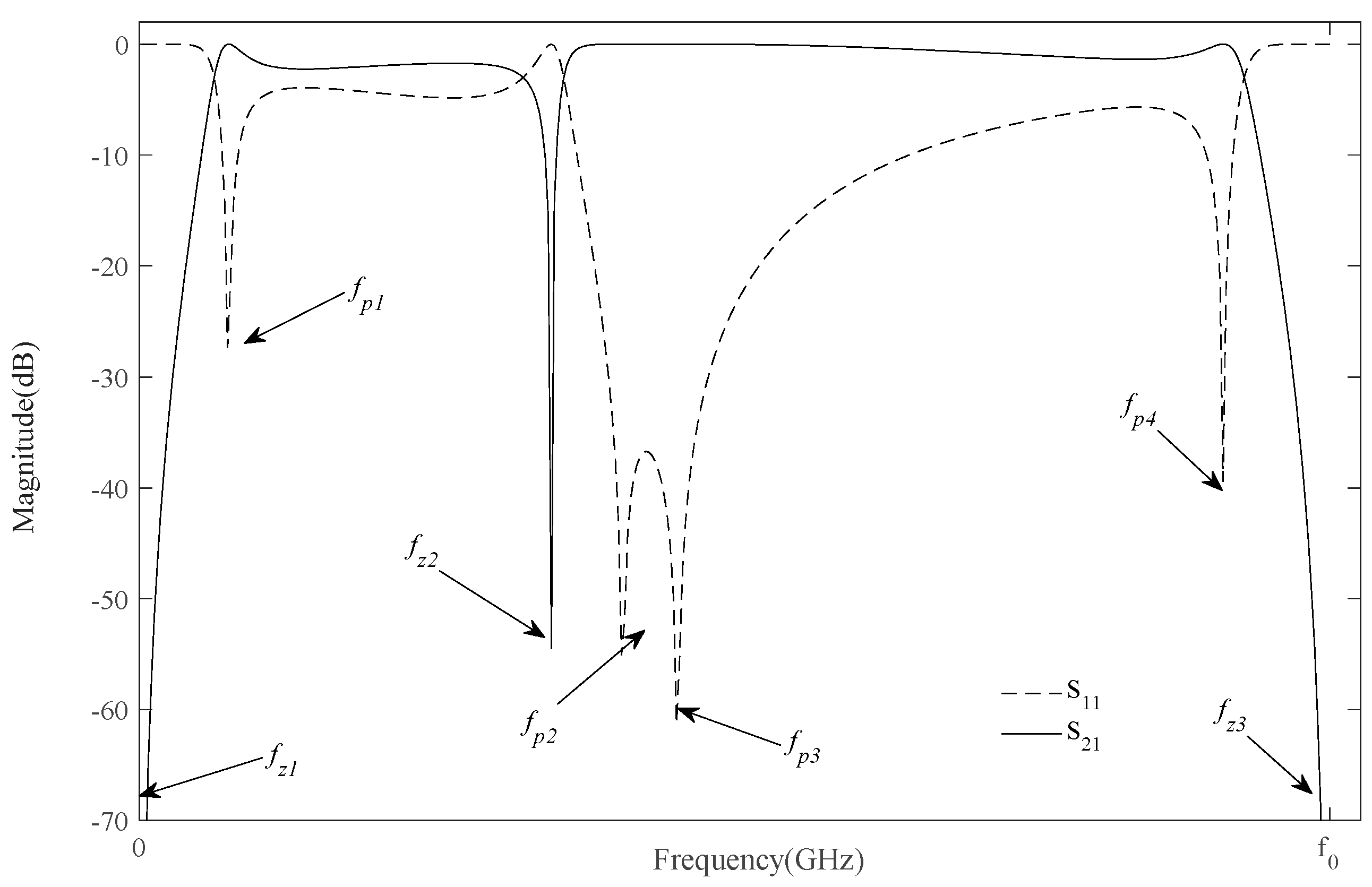
The transmission zeros of the CLCSR filter fulfill the conditions | S 21 | = 0 , which corresponds to z i n e = z i n o ( z L e = z L o ). When the value range of the parameter of θ 1 , θ 2 , θ 3 is in [ 0 , π ] , there are three transmission zeros: f z 1 , f z 2 , f z 3 . By assuming θ 1 = θ 3 = θ , f z 1 = 0 ( θ = 0 ) and f z 3 = f 0 ( θ = π ) do not change with the changing of the normalized impedances and the electrical length θ 2 . Meanwhile, by setting θ 1 = θ and θ 2 = θ / 2 , f z 3 = f 0 ( θ = π ) does not change with the changing of the normalized impedances and the electrical length θ 3 .
In order to simplify the calculation, the electrical length parameters θ 1 = θ 3 = θ and θ 2 = θ / 2 are set. According to the following resonant condition z L e = z L o , the transmission zero f z 2 can be obtained. When the transmission zero f z 2 of the CLCSR filter is close to the passband, the CLCSR filter selectivity is better, and the stopband bandwidth of the CLCSR filter is wider.
f z 2 = [ 2 f 0 arctan ( 2 z 4 z c e 2 + z c e 2 z c e 3 2 z 4 z c e 2 + 8 z 4 z c e 3 + z c e 2 z c e 3 ) ] π
By setting z i n o = or z i n e = , the transmission poles can be obtained. The odd-mode transmission pole f p 3 = f 0 / 2 is obtained when θ 1 is equal to π / 2 in Equation (1). The transmission pole f p 3 is only related to the electrical length θ 1 .
The even mode resonant condition is z i n e = and the even mode transmission poles can be obtained through Equation (5):
1 k 1 2 z 1 + j ( 1 k 1 2 ) z L e ( o ) tan θ = 0
By solving Equation (5), there are three transmission poles in the frequency range [ 0 , π ] , which are f p 1 , f p 2 , and f p 4 .
Figure 2 shows the distribution of the transmission poles and transmission zeros in the frequency range [0, f 0 ]. The numbers and relative positions of the transmission zeros and transmission poles are shown in Equation (6).
f z 1 < f p 1 < f z 2 < f p 2 < f p 3 < f p 4 < f z 3
The transmission zero f z 2 is affected by the parameters z c e 2 and z c e 3 .The impedance parameters and coupling coefficient of the CLCSR filter are assumed as k 1 = 0.8 , z 1 = 0.5 , z 4 = 2 , z c e 2 = 2.8 , z c e 3 = 2.4 . From Figure 3, when the value of z c e 2 increases, f z 2 moves to high frequency and the CLCSR filter’s bandwidth decreases. Meanwhile, with the increase of z c e 3 , f z 2 moves to low frequency and the proposed CLCSR’s bandwidth increases.
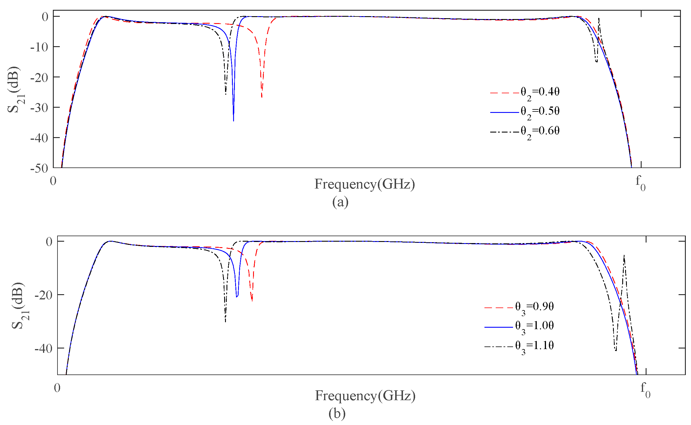
The transmission zero f z 2 is also affected by parameters θ 2 and θ 3 . The frequency responses of f z 2 with different θ 2 and θ 3 are shown in Figure 4 under the basic design parameters of k 1 = 0.8 , z 1 = 0.5 , z 4 = 2 , z c e 2 = 2.8 , z c e 3 = 2.4 . As the values of θ 2 or θ 3 increase, f z 2 moves to low frequency and the CLCSR filter’s bandwidth increases. θ 2 and θ 3 does not significantly affect f z 1 and f z 3 .

2.3. Transmission Poles Analysis

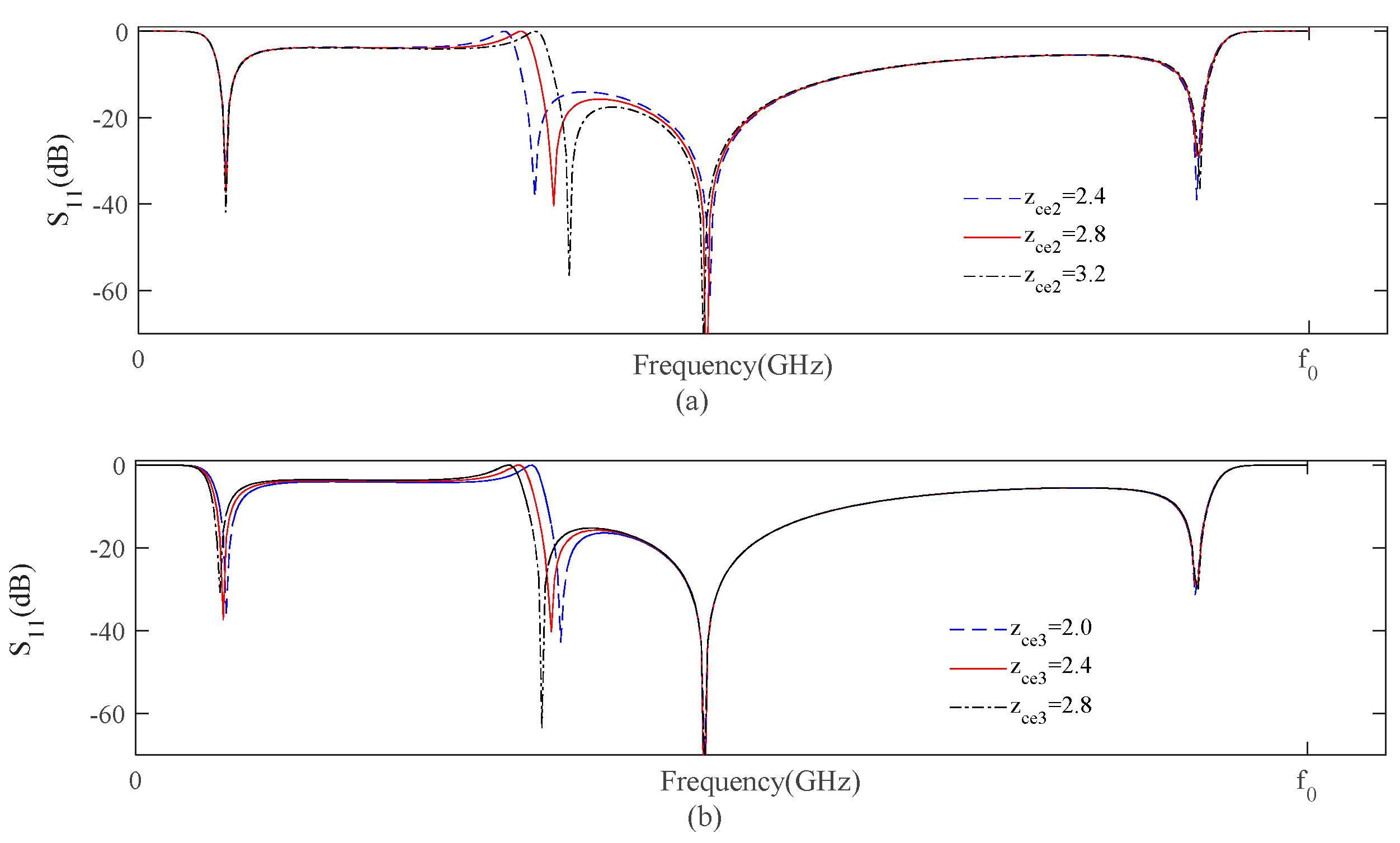
The transmission poles are affected by parameters z c e 2 and z c e 3 . In Figure 5a, the transmission pole f p 2 moves to high frequency and the CLCSR filter’s bandwidth decreases as z c e 2 increases. In Figure 5b, as z c e 3 increase, the transmission pole f p 2 moves to low frequency and the proposed CLCSR filter’s bandwidth increases. At the same time, the frequency responses of the transmission poles f p 3 and f p 4 are basically unchanged.
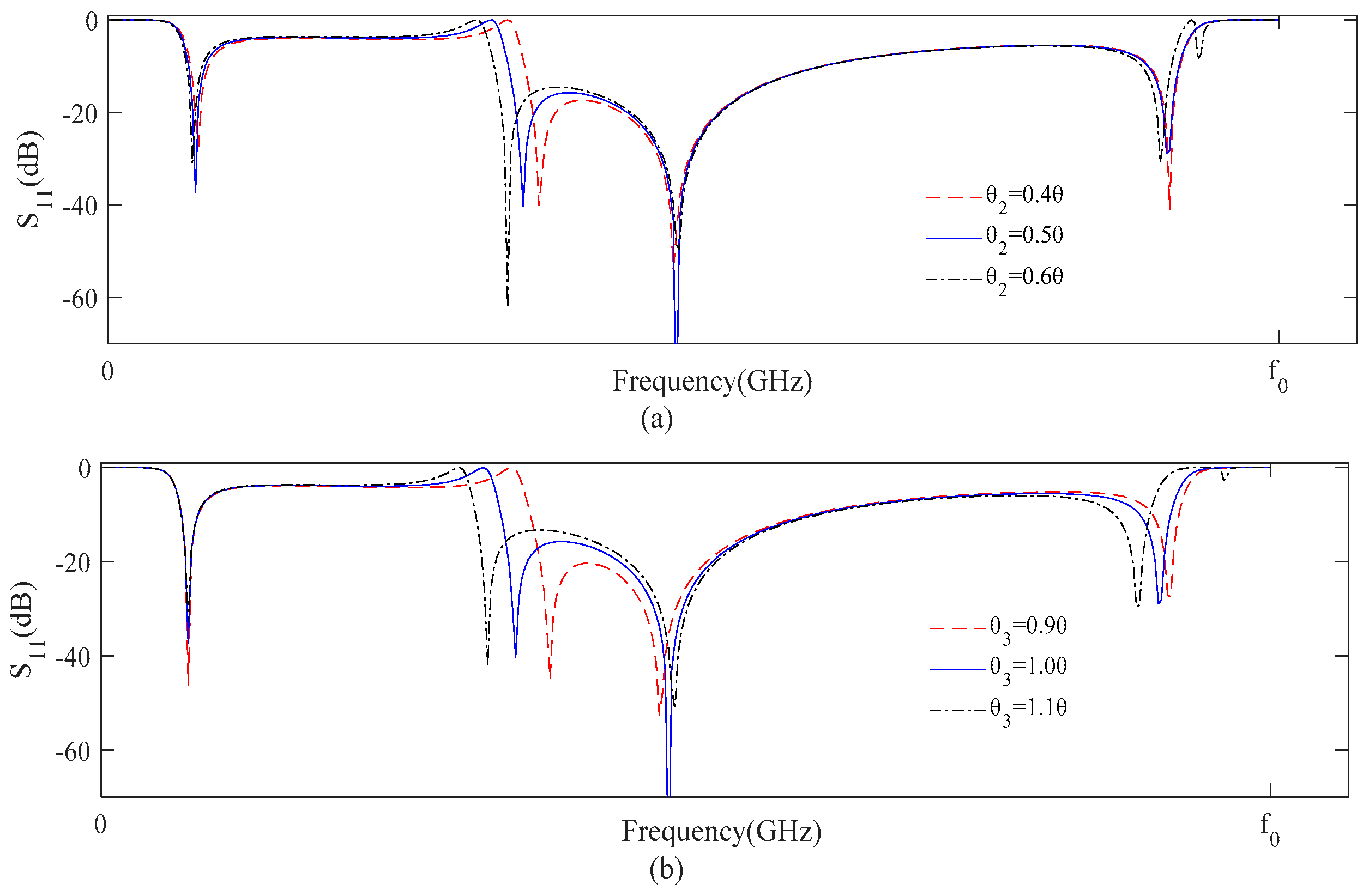
The transmission poles are also affected by parameters θ 2 and θ 3 . The transmission poles f p 2 and f p 4 affect the bandwidth of the proposed CLCSR filter, so two transmission poles are discussed. In Figure 6a, with the increase of θ 2 , the transmission poles f p 2 and f p 4 move to low frequency. The proposed CLCSR filter’s bandwidth increases with the increase of θ 2 . However, the change of the transmission pole f p 4 is small. In Figure 6b, as the value of θ 3 increases, the transmission pole f p 2 moves to low frequency and the frequency of the transmission pole f p 4 is basically unchanged. With the increase of θ 3 , the proposed CLCSR filter’s bandwidth increases.

3. Filter’s Results and Discussion

3.1. Filter’s Results

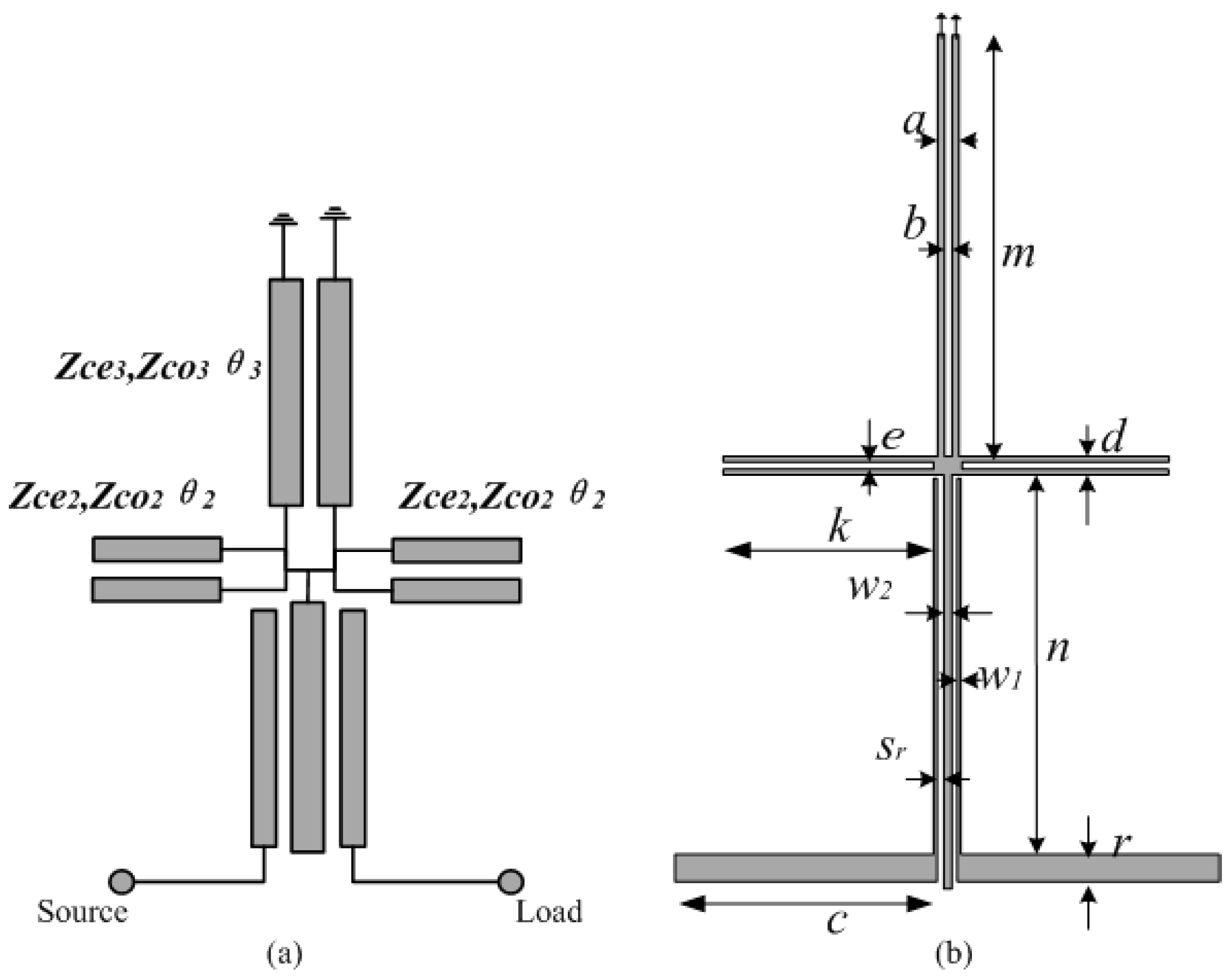
The coupling coefficient of the parallel coupled line feed structure is about equal to 0.8, so the distance between parallel coupled lines is too small to be fabricated. Therefore, the parallel-coupled line feed structure and the single-branch microstrip line are replaced with the three microstirp lines coupled structure based on Ref. [12]. As the equivalent circuit of the proposed bandpass filter shown in Figure 7a, the parallel coupled line feed structure is replaced with the three microstirp lines coupled structure.
The proposed bandpass filter is designed on Rogers RT5880 microwave dielectric board ( h = 0.508   mm   , ε r e = 2.2 , tan δ = 0.0009 ), whose f 0 is 4.4   GHz . Based on the impedance parameters, electric lengths and coupling coefficient of the proposed bandpass filter’s equivalent circuit, the initial physical parameters of the proposed bandpass filter are as follows: a = 1.08   mm , b = 0.16   mm , c = 14.60   mm , d = 0.78   mm , e = 0.18   mm , k = 11.5   mm , n = 21.6   mm , m = 23.4   mm , r = 1.54   mm .
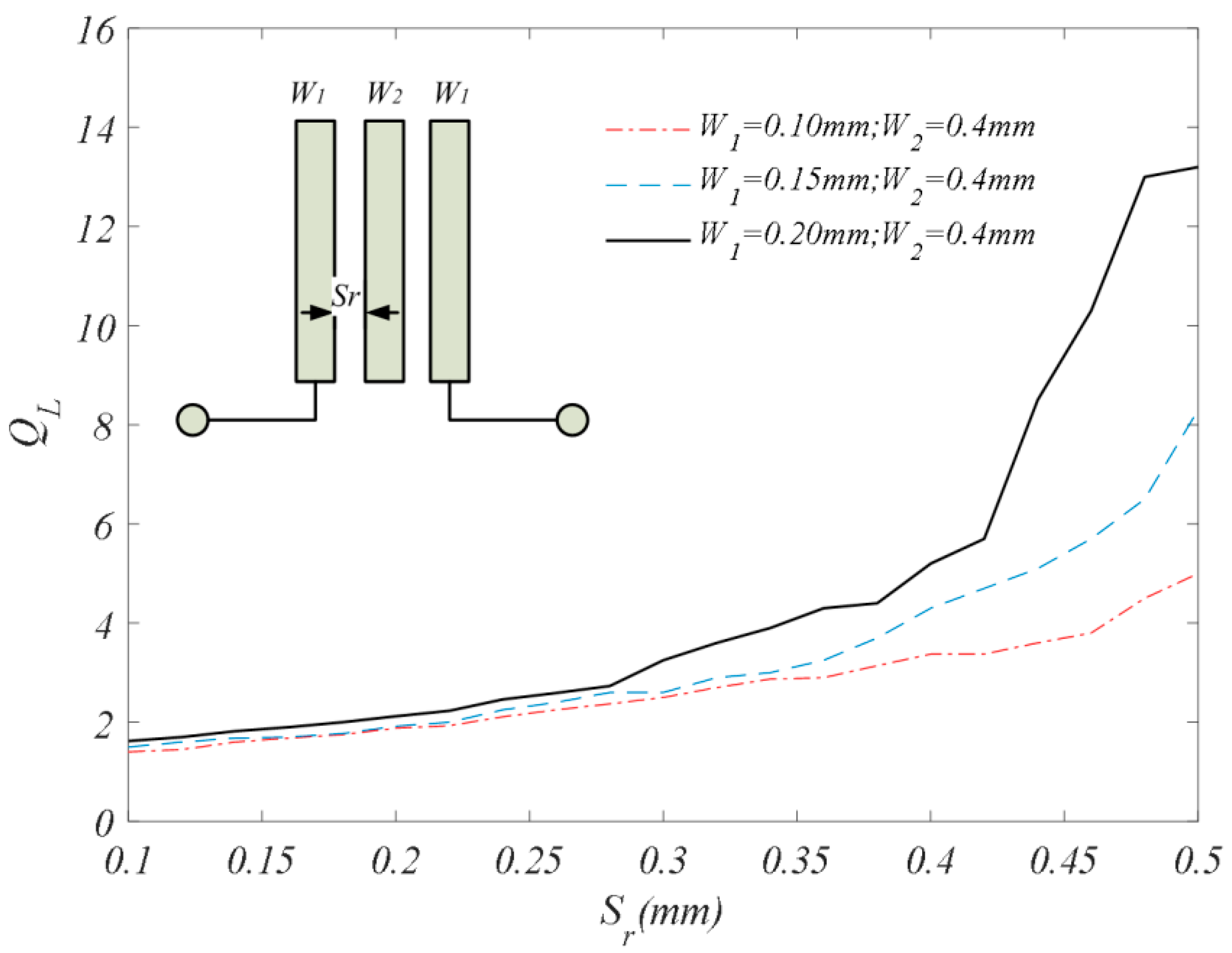
As shown in Figure 8, the influence between the structural parameters of the three microstirp lines coupled structure and the quality factor Q L is analyzed. From Figure 8, when S r is less than 0.3 mm, the values of W 1 and S r have little effect on Q L .
The resonant characteristics of the proposed bandpass filter are simulated by using ANSYS HFSS. The final physical parameters of the proposed bandpass filter are shown in Figure 7b: a = 0.9   mm , b = 0.16   mm , c = 14.6   mm , d = 0.7   mm , e = 0.16   mm , w 1 = 0.15   mm , w 2 = 0.15   mm , s r = 0.15   mm k = 11.5   mm , r = 1.54   mm , m = 23.4   mm , n = 21.6   mm .
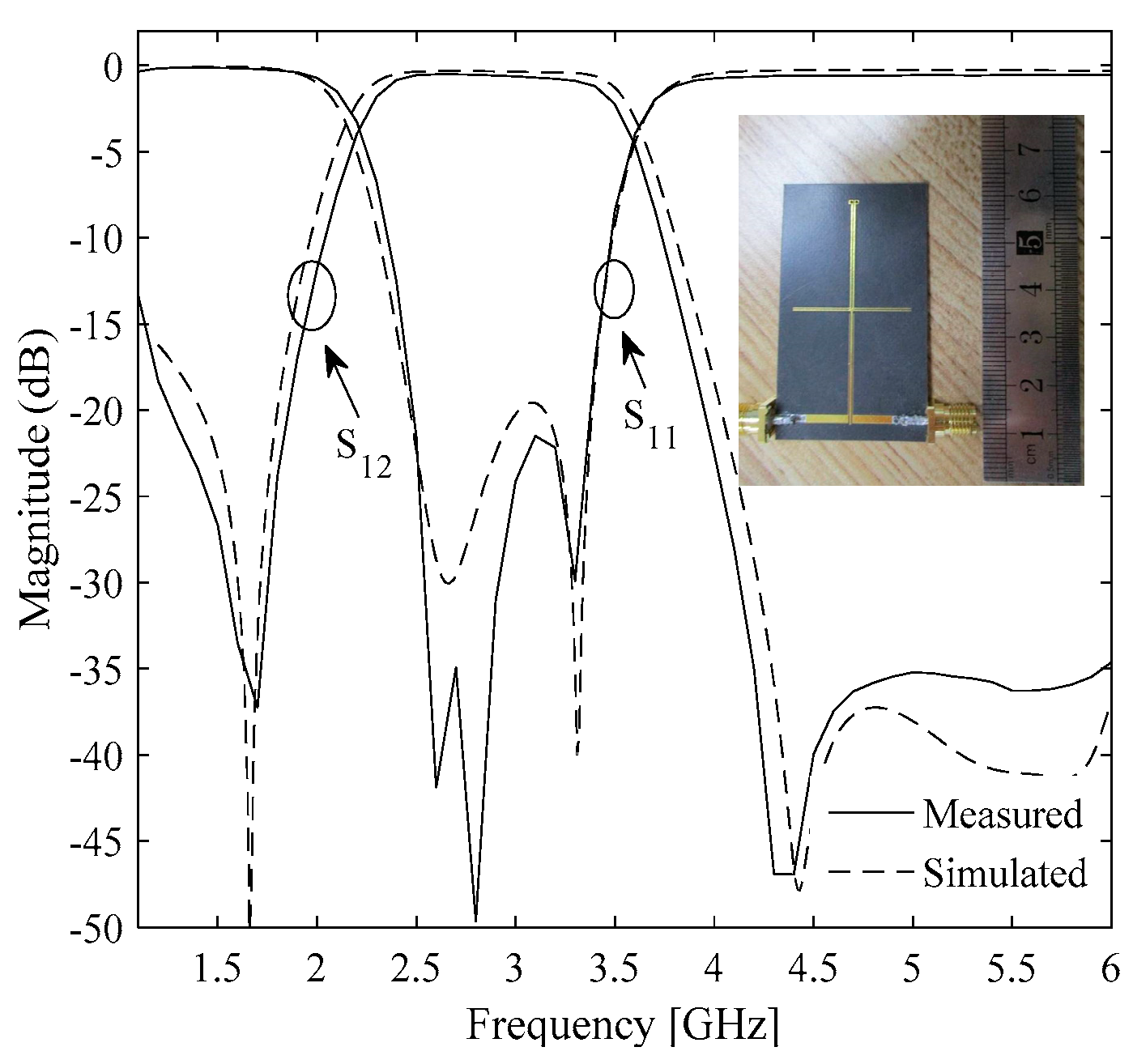
The simulated and measured results of the fabricated bandpass filter are illustrated in Figure 9. In the measured results, the center frequency is 2.95 GHz, and the 3-dB bandwidth is about 1.5 GHz. In the passband, the measured insertion loss (IL) is less than 0.4 dB, while the return loss (RL) is greater than 20 dB. Furthermore, the rejection levels of over 35 dB at the upper stop band from 4.4 to 6 GHz have been achieved. From 1 to 2 GHz, the out-of-band rejection levels are greater than 15 dB.

3.2. Filter Performance Discussion

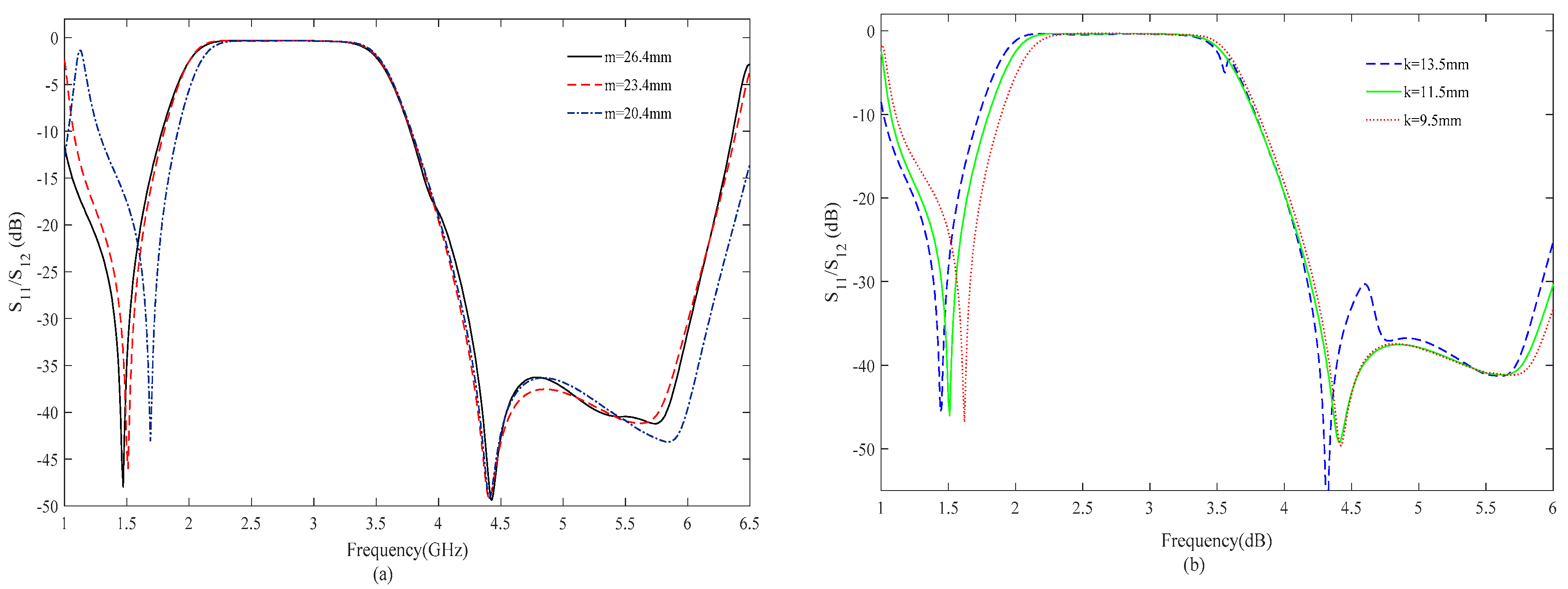
The bandwidth of the proposed bandpass filter can be adjusted by changing the θ 2 and θ 3 , independently. Figure 10 shows the resonant characteristics of the proposed bandpass filter with different lengths m and k . In Figure 10a, it is noted that when m decreases from 26.4 mm to 20.4 mm, the frequency of the transmission zero f z 2 increases from 1.47 GHz to 1.70 GHz. From Figure 10b, the frequency of the transmission zero f z 2 increases from 1.43 GHz to 1.63 GHz when k decreases from 13.5 mm to 9.5 mm. With the increase of m or k , the bandwidth of the bandpass filter gets wider.
The surface current distributions at the critical frequencies are shown in Figure 11. Current distributions are used to further research the effects of different sections on its frequency response.
Table 1 gives the performance comparisons of the proposed bandpass filter with some previous works. The proposed bandpass filter is compact. The return loss and insertion loss in passband are better than others. The proposed bandpass filter has better out of band rejection. There are two transmission zeros and the frequency selectivity is better.

4. Conclusions

In this paper, a cross-coupled line wide bandpass filter is proposed. With the use of the even and odd-mode approach, the transmission zeros and transmission poles of the proposed bandpass filter are analyzed and discussed. A three microstirp line coupled structure is used to increase coupling coefficient and make the filter compact. This structure also can improve stopband characteristics. The bandwidth can be adjusted by changing the length of the short-end parallel coupled line or the open-end parallel coupled line. Finally, the resonant characteristics of the proposed bandpass filter are measured. Good agreement between the simulations and measurements is obtained, which validates the design method.

Author Contributions

D.-S.L., X.G., and Y.-Y.L. designed the method and wrote the paper; S.-M.C. and J.-W.G. performed the experiments and analyzed the data. All authors have read and agreed to the published version of the manuscript.

Funding

This work was supported by the National Natural Science Foundation of China (61501100), the Fundamental Research Funds for the Central Universities (N2023017), and Natural Science Foundation of Hebei Province (F2019203012).

Conflicts of Interest

The authors declare that there is no conflict of interest regarding the publication of this paper.

References

  1. Wang, H.; Yang, G.; Kang, W.; Miao, C.; Wu, W. Application of Cross-Shaped Resonator to the Ultra Wideband Bandpass Filter Design. IEEE Microw. Wirel. Components Lett. 2011, 21, 667–669. [Google Scholar] [CrossRef]
  2. Da Xu, K.; Zhang, F.; Liu, Y.; Nie, W. High Selectivity Seventh-order Wideband Bandpass filter Using Coupled Lines and Open-sorted Stubs. Electron. Lett. 2018, 54, 223–225. [Google Scholar]
  3. Xu, K.-D.; Li, D.; Liu, Y. High-Selectivity Wideband Bandpass Filter Using Simple Coupled Lines With Multiple Transmission Poles and Zeros. IEEE Microw. Wirel. Components Lett. 2019, 29, 107–109. [Google Scholar] [CrossRef]
  4. Li, L.; Li, Z.-F. Side-Coupled Shorted Microstrip Line for Compact Quasi-Elliptic Wideband Bandpass Filter Design. IEEE Microw. Wirel. Components Lett. 2010, 20, 322–324. [Google Scholar] [CrossRef]
  5. Ahmadi, A.; Makki, S.V.; Lalbakhsh, A.; Majidifar, S. A Novel Dual-Mode Wideband Bandpass Filter. ACES J. 2014, 29, 735–742. [Google Scholar]
  6. Lalbakhsh, A.; Jamshidi, M.B.; Siahkamari, H.; Ghaderi, A.; Golestanifar, A.; Linhart, R.; Talla, J.; Simorangkir, R.B.; Mandal, K. A compact lowpass filter for satellite communication systems based on transfer function analysis. AEU Int. J. Electron. Commun. 2020, 124, 153318. [Google Scholar] [CrossRef]
  7. Zhang, W.; Feng, F.; Zhang, J.; Zhao, Z.; Ma, J.; Zhang, Q. Parallel Decomposition Approach to Wide-Range Parametric Modeling With Applications to Microwave Filters. IEEE Trans. Microw. Theory Tech. 2020, 68, 5288–5306. [Google Scholar] [CrossRef]
  8. Sheikhi, A.; Alipour, A.; Mir, A. Design and Fabrication of an Ultra-Wide Stopband Compact Bandpass Filter. IEEE Trans. Circuits Syst. II Express Briefs 2019, 67, 265–269. [Google Scholar] [CrossRef]
  9. Rao, Y.; Qian, H.J.; Yang, B.; Gomez-Garcia, R.; Luo, X. Dual-Band Bandpass Filter and Filtering Power Divider With Ultra-Wide Upper Stopband Using Hybrid Microstrip/DGS Dual-Resonance Cells. IEEE Access 2020, 8, 23624–23637. [Google Scholar] [CrossRef]
  10. Guo, Z.-C.; Zhu, L.; Wong, S.-W. A Quantitative Approach for Direct Synthesis of Bandpass Filters Composed of Transversal Resonators. IEEE Trans. Circuits Syst. II Express Briefs 2018, 66, 577–581. [Google Scholar] [CrossRef]
  11. Bi, X.-K.; Cheng, T.; Cheong, P.; Ho, S.-K.; Tam, K.-W. Design of Dual-Band Bandpass Filters with Fixed and Reconfigurable Bandwidths Based on Terminated Cross-Shaped Resonators. IEEE Trans. Circuits Syst. II: Express Briefs 2018, 66, 317–321. [Google Scholar] [CrossRef]
  12. Bi, X.-K.; Teng, C.; Cheong, P.; Ho, S.-K.; Tam, K.-W. Wideband bandpass filters with reconfigurable bandwidth and fixed notch bands based on terminated cross-shaped resonator. IET Microw. Antennas Propag. 2019, 13, 796–803. [Google Scholar] [CrossRef]
  13. Feng, W.; Che, W. Wideband balanced bandpass filter based on three-line coupled structure. Electron. Lett. 2012, 48, 1006–1008. [Google Scholar] [CrossRef]
  14. Lalbakhsh, A.; Alizadeh, S.M.; Ghaderi, A.; Golestanifar, A.; Mohamadzade, B.; Jamshidi, M.B.; Mandal, K.; Mohyuddin, W. A Design of a Dual-Band Bandpass Filter Based on Modal Analysis for Modern Communication Systems. Electronics 2020, 9, 1770. [Google Scholar] [CrossRef]
  15. Moradi, B.; Fernández-García, R.; Gil, I. Meander Microwave Bandpass filter on a Flexible Textile Substrate. Electronics 2019, 8, 11. [Google Scholar] [CrossRef] [Green Version]
  16. Xu, J.; Miao, C.; Wu, W. A compact and high isolation dual-mode dual-band bandpass filter with tunable transmission zeros. J. Electromagn. Waves Appl. 2012, 26, 2390–2397. [Google Scholar] [CrossRef]
  17. Wang, H.; Gao, L.M.; Tam, K.W.; Kang, W.; Wu, W. A Wideband Differential Bandpass Filter With Multiple Differential- and Common-Mode Transmission Zeros Using Cross-Shaped Resonator. IEEE Microw. Wirel. Compon. Lett. 2014, 24, 854–856. [Google Scholar] [CrossRef]
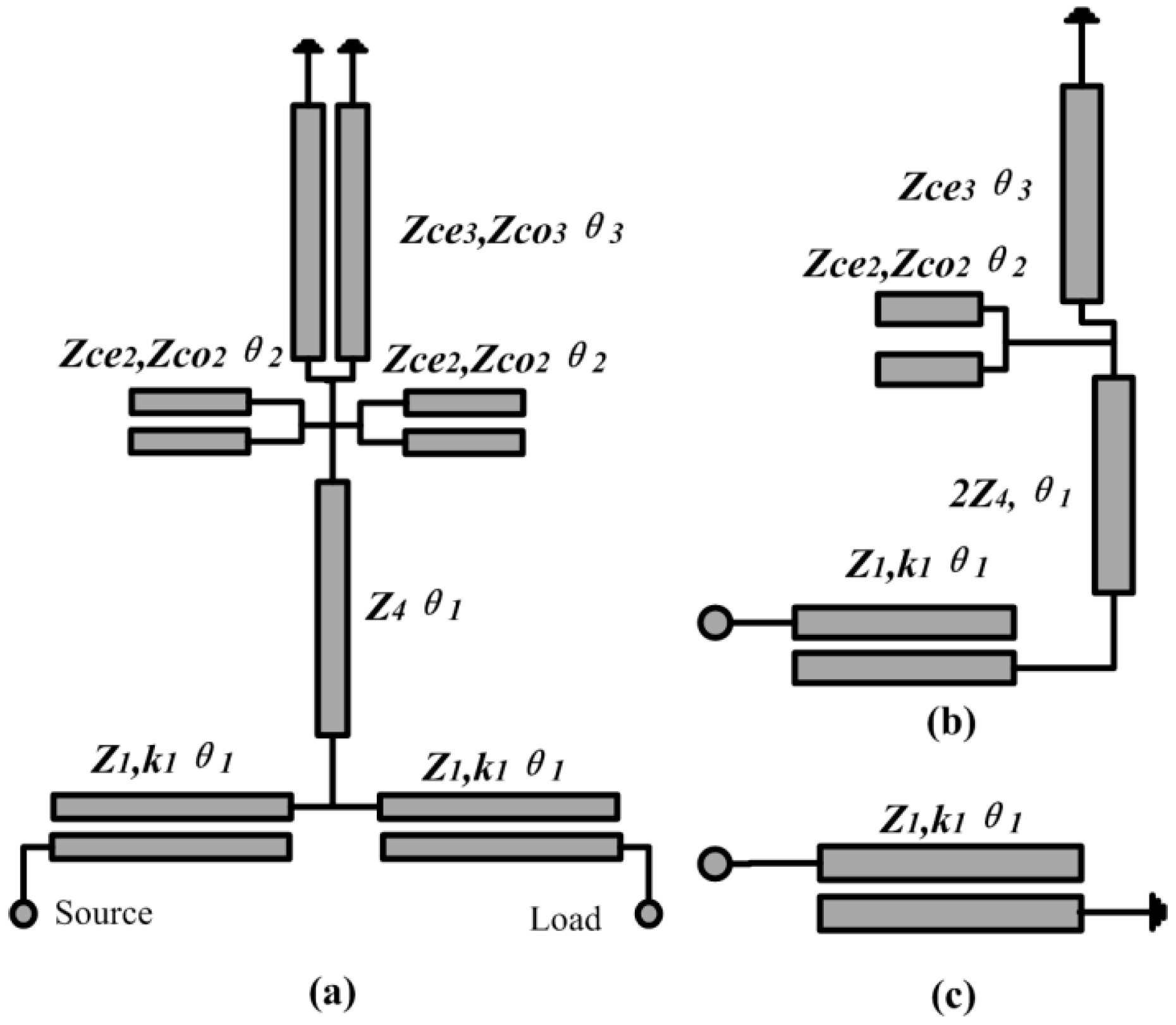
Figure 1. Ideal circuit of the CLCSR and its equivalent circuit model, (a) Ideal circuit model, (b) Even-mode circuit, (c) Odd-mode circuit.
Electronics 09 02173 g001
Figure 2. Calculated frequency responses of the ideal circuits shown in Figure 1.
Electronics 09 02173 g002
Figure 3. Simulated frequency responses of the CLCSR filter with varied designing parameters z c e 2 and z c e 3 .
Electronics 09 02173 g003
Figure 4. Simulated frequency responses of the proposed CLCSR filter with varied parameters, (a) θ 2 and (b) θ 3 .
Electronics 09 02173 g004
Figure 5. Simulated frequency responses of the proposed CLCSR filter with varied parameters (a) z c e 2 and (b) z c e 3 .
Electronics 09 02173 g005
Figure 6. Simulated frequency responses of the proposed CLCSR filter with varied parameters (a) θ 2 and (b) θ 3 .
Electronics 09 02173 g006
Figure 7. (a) The equivalent circuit of the proposed bandpass filter; (b) The design size of the proposed bandpass filter.
Electronics 09 02173 g007
Figure 8. Effect of three-line width on quality factor.
Electronics 09 02173 g008
Figure 9. Simulated and measured results of the fabricated bandpass filter.
Electronics 09 02173 g009
Figure 10. Bandwidth control of the proposed bandpass filter at lower band frequency by (a) m and (b) k .
Electronics 09 02173 g010
Figure 11. Current density distributions of the proposed bandpass filter at different frequencies: (a) 2.5 GHz, (b) 2.8 GHz, (c) 3.2 GHz.
Electronics 09 02173 g011
Table 1. Comparisons with Some Previous Bandpass Filters.
Ref.Center Frequency (GHz)Lower Stopband (dB)Upper Stopband (dB)RL (dB)IL (dB)Size
( λ g   ×   λ g )
[1]6.65<−20<−20200.350.5 × 0.79
[2]1.93<−40<−35200.40.56 × 0.23
[3]2.05<−32<−20200.60.48 × 0.24
[5]8.28<−20<−25151.91.12 × 0.45
[10]3<−10<−18161.280.18 × 0.175
[13]6.71<−30<−25151.450.5 × 0.04
[14]7.6<−20<−10160.60.64 × 0.31
This work2.95<−15<−35200.40.12 × 0.23
Publisher’s Note: MDPI stays neutral with regard to jurisdictional claims in published maps and institutional affiliations.