Abstract
Wireless power transmission (WPT) using an inductively coupled link is one of the most popular approaches to deliver power wirelessly to biomedical implants. As the electromagnetic wave travels through the tissue, it is attenuated and absorbed by the tissue, resulting in much weaker electromagnetic coupling than in the air. As a result, the received input power on the implant is very weak, and so is the input voltage at the rectifier, which is the first block that receives the power on the implant. With such a small voltage amplitude, the rectifier inevitably has a very poor power conversion efficiency (PCE), leading to a poor power transfer efficiency (PTE) of the overall WPT system. To address this challenge, we propose a new system-level WPT method based on duty cycling of the power transmission for millimeter-scale implants. In the proposed method, the power transmitter (TX) transmits the wave with a duty cycle. It transmits only during a short period of time and pauses for a while instead of transmitting the wave continuously. In doing so, the TX power during the active period can be increased while preserving the average TX power and the specific absorption rate (SAR). Then, the incoming voltage becomes significantly larger at the rectifier, so the rectifier can rectify the input with a higher PCE, leading to improved PTE. To investigate the design challenges and applicability of the proposed duty-cycled WPT method, a case for powering a 1 × 1-mm-sized neural implant through the skull is constructed. The implant, a TX, and the associated environment are modeled in High-Frequency Structure Simulator (HFSS), and the circuit simulations are conducted in Cadence with circuit components in a 180-nm CMOS process. At a load resistor of 100 k, an output capacitor of 4 nF, and a carrier frequency of 144 MHz, the rectifier’s DC output voltage and PCE are increased by 300% (from 1.5 V to 6 V) and by 50% (from 14% to 64%), respectively, when the duty cycle ratio of the proposed duty-cycled power transmission is varied from 100% to 5%.
1. Introduction
Wireless power transfer (WPT) has become one of the most promising power transmission schemes for various biomedical implants as it obviates the need for bulky batteries and, consequently, invasive battery replacement surgeries [1,2,3,4]. Among multiple WPT methods for biomedical implants such as inductive powering [5], capacitive powering [6], optical powering [7], and ultrasonic energy transferring [8], inductive powering is one of the most developed and popular approaches to deliver power wirelessly over a-few-cm distances [1,4,9,10]. However, this technique suffers from low power transfer efficiency (PTE) when used for millimeter-scale implants because of the poor electromagnetic coupling between the external power transmitter and the implant’s coil antenna [11]. The PTE largely depends on the coupling coefficient k and the quality factor Q of the coils. Both of them are drastically degraded as the coil antenna size is scaled down to millimeter scales [11,12]. For millimeter-scale free-floating implants, an achievable Q factor on the implant side is typically around or below 10. Thus, an achievable k is around or less than 0.005, and the resulting PTE is only 2% or less [13,14]. Hence, low achievable PTEs remain one of the most limiting bottlenecks for further miniaturization of implants.
In addition to such poor electromagnetic coupling, the absorption of electromagnetic waves by biological tissues confines the maximum transmittable power, thus further limiting the power delivered to the load (PDL) [15]. The international safety standards on specific absorption rate (SAR) limit the transmitted power of TX to 1.6 W/kg according to the IEEE guidelines [16]. SAR is the parameter commonly used to quantify absorptive and exposure levels of biological tissue to electromagnetic waves. Due to these reasons, therefore, the input power at the implant is typically very weak.
1.1. PTE-Improvement Techniques for Inductively Coupled WPT Systems
To improve the amount of power delivered to the biomedical implants and the efficiency, various techniques have been proposed and demonstrated. As one of the most basic techniques, impedance matching should be properly achieved for high PTEs. To obtain a proper impedance matching, an inductance tapping circuit and a voltage doubler circuit were proposed [17]. For the robust operation of the inductive link, various tuning techniques were also demonstrated [17,18,19]. As it is difficult to achieve a high Q for the coil on the miniature biomedical implant, some techniques to increase the inductance on the implant side were proposed [20,21,22,23]. Besides, techniques to optimize the design parameters of the planar printed spiral coils were demonstrated, achieving a PTE of 41.2% with a link operating frequency of 1 MHz [22]. In [20], a micro-coil array was implemented for a multi-channel wireless implantable system to achieve a high PTE. Similarly, a three-coil inductive link was proposed to achieve both high PTE and PDL [23]. However, an extra coil generally requires a larger space on the implant side and more complex designs, posing several design constraints on the inductor geometries [24].
1.2. Techniques to Improve the Power Conversion Efficiency of Rectifiers
To improve the overall PTE, many recent studies have investigated the rectifier circuits. Because the rectifier is the first power-receiver block on the implant side, the rectifier should extract as much power as possible from the RF input. Rectifiers convert the incoming RF input to a DC voltage () at the output. The power conversion efficiency (PCE) of a rectifier is the ratio of the DC output power to the input power of the rectifier [25]. The PCE largely depends on its circuit topology, diode-device parameters, RF input power, and output loading conditions. Comparators can be used to turn on and off the MOSFETs to improve the PCE [26]. However, they typically work at relatively low frequencies as 13.56 MHz, and they are in-efficient at high frequencies. For millimeter-sized implants, typical carrier frequencies are over 100 MHz and even above 1 GHz [12,27,28]. The rectifiers for such applications are typically made up with passive components. For most passive rectifier topologies, the threshold voltage () of the diode devices is the major limiting factor of the PCE [29], especially when the input signal’s amplitude is small. Diode-based rectifiers typically suffer from a huge voltage drop across the diodes, leading to a poor PCE and wide dead zone at low input levels. As compared to typical pn-junction diodes and MOSFET-based diodes, using Schottky diodes in a rectifier can enhance its PCE, especially at low input power, because of their very small threshold voltage and fast switching speeds [30,31,32]. The fully cross-coupled rectifier [25] can alleviate the dead-zone problem (the input sensitivity problem) to some extent and operate at a relatively low input power by applying the input signal deferentially across the four rectifying transistors. However, it suffers from a poor PCE due to the presence of reverse leakage currents.
Even with recent improvements in rectifier circuits [29,33,34,35], the improvement in the PCE and eventually in the PTE is still not enough. The input sensitivity issue caused by the dead zone is not resolved. To address the aforementioned challenges of low PCE and PTE at weak input power and the dead-zone issue, we present a new system-level WPT method utilizing a duty-cycled WPT technique that significantly improves the PCE and wireless power delivery to the miniature biomedical implants at low input power levels. Similar preliminary works were presented previously [36,37,38]. Compared to these, our paper includes more systematic analyses on the method from the rectifier to the whole system, mathematical derivations on the optimal load condition, and practical considerations in various aspects. Details of the proposed method are presented in the next section. The validation setup, including the design specifications of the HFSS circuit models, is described in Section 3. Section 4 shows the results of simulations using a 1 × 1-mm implant model and discusses main practical constraints of the proposed schemes. Section 5 concludes the paper.
2. The Proposed Scheme
Figure 1 shows an overall circuit diagram of a general WPT system, which includes a transmitter (TX), receiver (Rx), and biological tissue in between. The two coils, and , are inductively coupled with a coupling coefficient k. The LC tanks on both sides are tuned to resonate at the same resonant frequency with and , respectively. The LC tank on the secondary side is connected to a rectifier, which generates a DC voltage to the load . The figure also illustrates voltage waveforms of major nodes (, and ) for the conventional and the proposed power transmission methods. As compared to the conventional WPT method where the power is continuously transmitted, in the proposed duty-cycled power transmission, the RF power signal is transmitted during a designated portion of time only and remains dormant for the rest of the duration. The active and dormant periods are iterated with a periodic interval of , as shown in Figure 2. Figure 2 shows the relationship between and the active duty period () of the duty-cycled waveform. The ratio of these two is the duty cycle ratio D, which is given as follows:
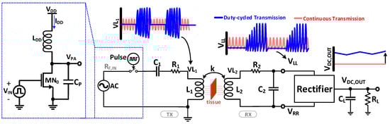
Figure 1.
Circuit diagram of the general wireless power transmission (WPT) system with waveforms of major voltage nodes for the conventional continuous power transmission (in red) and the proposed duty-cycled power transmission (in blue). Inset: Implementation scenario with a class-E amplifier for the input voltage control.
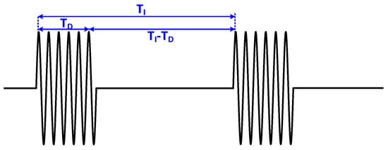
Figure 2.
Duty-cycled waveform with indications of the duty cycle interval and the active duty period .
As illustrated in Figure 1, the instantaneous TX power for the proposed method can be larger than that of the conventional continuous power transmission at the same RF input. The TX power for the proposed method is increased up to the point where the average TX power is the same as that of the continuous powering case. Then, the average SAR levels of both cases are at the same level. As a result, the rectifier’s voltage input is also increased, so a greater proportion of the input can more easily overcome the threshold voltage of the rectifier. Hence, more RF power is converted into the output DC power with a higher PCE of the rectifier, effectively increasing the overall PCE of the rectifier circuit and the output DC voltage level and the PTE of the WPT system.
3. Validation Setup
3.1. HFSS Simulation Model
To validate the proposed scheme, we constructed a three-dimensional finite element method (FEM) model in Ansys HFSS, as shown in Figure 3. The model models multi-layered brain tissues, including the skull, based on frequency-dependent dielectric properties [12]. An 1 × 1-mm-sized implant, which is assumed to be a 200-m-thick semiconductor chip fabricated in a CMOS Silicon-on-Insulator (SOI) process (XFAB XT018), is covered with Parylene C and placed on the grey matter under the skull at a depth of 9.7 mm. The top view of the RX coil is shown in Figure 3. The 7-turn RX coil occupies the peripheral space of 1 × 1 mm of the implant. The widths of the metal coil and gap are kept at 1:1 while the center part (the area not occupied by the coil) is 0.5 × 0.5 mm. A single-turn power TX coil is positioned concentrically with the implant coil above the skin at an air-gap of 1 mm. The TX coil has a radius of 12 mm. The detailed geometry of the TX coil is also shown in Figure 3. Using this HFSS model, simulations were performed at the carrier frequency 144 MHz. With the two-port vector network analyzer in HFSS, Z parameters were obtained from the simulations. , , , and k values were calculated with the following equations:
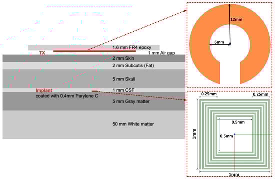
Figure 3.
Cross-sectional configuration of the implemented finite element method (FEM) model in High-Frequency Structure Simulator (HFSS). The 1 × 1 mm-sized seven-turn-coil implant is placed at 9.7-mm depth of the brain. The one-tern circular transmitter (TX) is placed above the skin.
The following circuit parameters for both the TX and RX coils were acquired and used for the circuit simulations in Cadence: = 18.3 nH, = 0.285 , = 57.6 nH, = 6.78 , = 38.3 pF, = 12.2 pF, k = 0.00136. The resonance frequency is set at 144 MHz.
3.2. Rectifier Circuit and Characterization Results
On the RX side, the LC tank is connected to a rectifier. The rectifier in Figure 4 is chosen for validation of the proposed scheme, while the proposed method can be applied to most types of rectifiers in general. The rectifier is composed of a pair of Schottky diodes ( and ) and a pair of cross-coupled NMOS transistors ( and ). All of these circuit components are in a 180-nm CMOS SOI process. In the rectifier design, we selected Schottky diodes because of their low threshold voltage of 150–350 mV, much lower than typical pn junction diodes. Sizes of the NMOS transistors and Schottky diodes were optimized to acquire the maximum possible PCE at the given conditions.
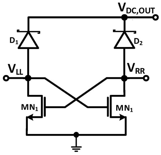
Figure 4.
Circuit diagram of the rectifier used in the validation.
Operational waveforms of the rectifier are shown in Figure 5. The input power to the rectifier is received through and during the active period of the duty-cycled powering. and are rectified during the active period, resulting in an increase of . During the dormant period of duty-cycled powering, droops slightly. To observe the rectifier operation more in detail during the positive and the negative cycles of and , these waveforms are zoomed in and shown in the inset of Figure 5. When is high and is low, it corresponds to the forward-biased condition for and . Because the gate voltage of is positive and high, has a small turn-on resistance. At the same time, overcomes the threshold voltage of , allowing the forward current to . The rectifier works for the other polarity vice versa.
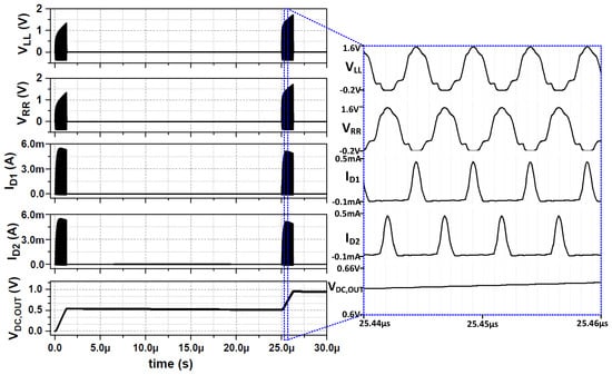
Figure 5.
Operational waveforms of the rectifier.
Before investigating the impacts of the duty-cycled power transmission on the PCE, PTE, and , the rectifier is characterized first. The amplitude of the input voltage on the primary side is varied from 0.1 V to 1.2 V at a fixed load resistor of and output capacitor of . The RF signal is transferred wirelessly to the secondary side and arrives at the input of the rectifier. The resulting , PCE, and PTE over the peak-to-peak voltage at the input of the rectifier are plotted in Figure 6. Here the PCE is the ratio of DC output power to the input power of the rectifier (PCE = / of the rectifier), and the PTE of a WPT system is the ratio of the DC output power to the input power of TX coil (PTE = / on the TX side). As shown in Figure 6a, linearly increases after a dead-zone of about 300 mV as increases. As shown in Figure 6b,c, the PCE and PTE also have a similar dead zone and increases monotonically afterwards as increases. When is 2 V, the resulting , PCE and PTE are 1.48 V, 14% and 0.0011%, respectively. As clearly shown in the results, this continuous power transmission suffers not only from its small outputs (, PCE, and PTE) but also from the dead-zone, which is ≈300 mV. When the RF input is within the dead zone, all , PTE, and PCE are stuck at zero.
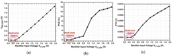
Figure 6.
Characterization results of the rectifier shown in Figure 4. (a) VDC,OUT, (b) power conversion efficiency (PCE), and (c) power transfer efficiency (PTE) of the rectifier with respect to VLL,ptp the peak-to-peak amplitude of the input voltage of the rectifier.
4. Results and Discussion
4.1. Circuit Simulation Setup
The circuit in Figure 1 was constructed in Cadence using the 180-nm CMOS SOI process. For each run of transient simulations, the circuit was simulated for a long enough duration to settle down at a steady state. For each simulation, , PCE of the rectifier, and PTE of the whole WPT system are observed. We simulated with the target circuit over from 0.1 V to 1.2 V for various duty cycle ratios, i.e., 100%, 50%, 10%, and 5%. For each duty cycle, the TX power should be maintained at the same level, so is the specific absorption rate (SAR). Since k is very small as 0.00136, the transmitted power is directly proportional to the power from the input source on the primary side. Thus, the input voltage required for each case of different duty cycle ratio is determined as follows:
where is for the case with 100% of duty cycle, and D is the duty cycle ratio. For instance, assume that the RF power is transmitted at 0.5 V of for a 100% duty cycle ratio. For D = 50%, the RF signal is transmitted only during half of the time, so the TX power can be doubled while maintaining the same SAR. Therefore, the required , in this case, is 0.707 V.
4.2. Simulation Results
The simulation results at = 100 k and = 4 nF for D = 100%, 50%, 10%, and 5% are shown in Figure 7. The results for 100% of the duty is the same as the conventional continuous power transmission. For all duty-cycle cases including the continuous transmission case, the average TX power is maintained at 25.5 dBm. Figure 7a clearly shows that significantly increases as D reduces for the all range of . increases by more than four times as D decreases from 100% to 5% for of 0.3 to 1.2 V. The increase in is attributed to the effective improvement in the rectifier’s PCE shown in Figure 7b. The maximum PCE is drastically increased from 14% to 64% at of 1.2 V. This inevitably leads to improvement in the overall PTE of the WPT system, as shown in Figure 7c. Moreover, as compared to the continuous power transmission (D = 100%), the proposed duty-cycled power transmission technique eliminates or significantly reduces the dead-zone for low-RF-input cases, as shown in the figures. In Figure 7d, the PCE of the rectifier is plotted with respect to the duty cycle ratio for various . As shown, significant improvements in the PCE are made by reducing the duty cycle ratio for every case. In addition, the proposed duty-cycled WPT system achieves 33% and 39% better PCE performances as compared to the previous PWM-based WPT techniques [37,38], respectively, at = 100 k.
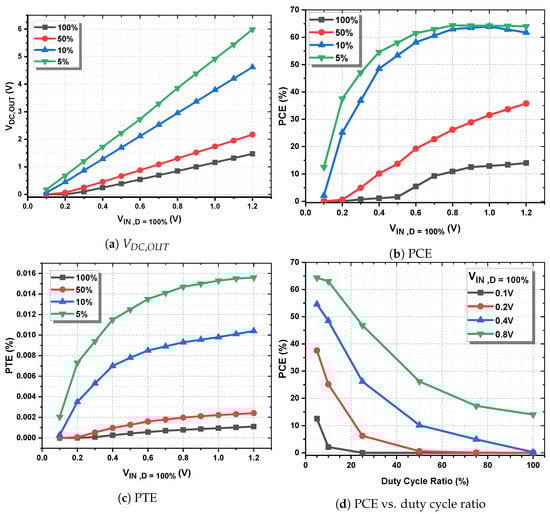
Figure 7.
Simulation results of the rectifier and the WPT system for various duty cycle ratios for the same amount of RF input power. (a) VDC,OUT, (b) PCE, and (c) PTE over VIN,D=100%. (d) PCE vs. duty cycle ratio for various VIN,D=100%.
To evaluate the effect of the duty cycle interval on the performance of the proposed method, simulations were done by sweeping from 1 s to 100 s for D of 100%, 50%, 10%, and 5%, at = 0.5 V, = 100 k, and = 4 nF. Figure 8 shows the resulting and PCE. is maintained for D = 50%, but it decreases as decreases for shorter duty cycle ratios. The decreasing slope is steeper for the case with . It is because it requires some recovery time to reach the maximum amplitude due to the resonance whenever the active transmission () starts. Figure 9 shows simulated and at at = 1 s and D = 5% ( = 0.05 s). The active duty period of the waveforms is zoomed in and shown on the right side of Figure 9. As shown, only several cycles of the RF carrier signal are sent for each duty interval (). Since is too short, the amplitude of the signals cannot reach the maximum level within . Due to this effect, decreases as decreases for small D (Figure 8a). On the contrary, the PCE is less affected by , as shown in Figure 8b.
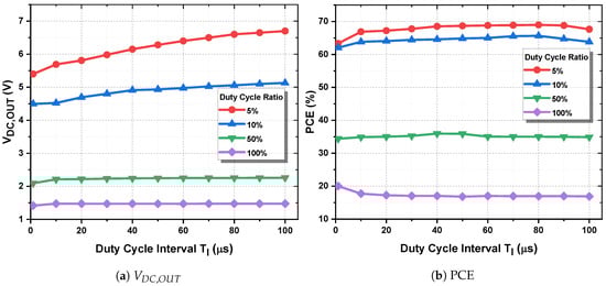
Figure 8.
(a) VDC,OUT and (b) PCE of the rectifier with respect to TI the duty cycle interval.
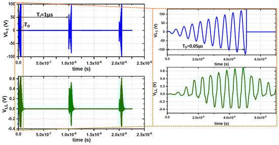
Figure 9.
Simulated and waveforms at = 1 s and D = 5%.
The performance gain by the duty-cycled power transmission depends on the load condition. The overall PTE of a WPT system strongly depends on the load, and the maximum power condition is differed by the load. Because the duty cycling effectively changes the load in view of the secondary LC tank and the overall WPT system, the duty cycle ratio and the load are interrelated. Hence, depending on the load condition, the PTE may not increase as the duty cycle ratio decreases. Therefore, the load conditions should also be considered to achieve the peak PTE.
The PTE of the WPT system is evaluated under various load conditions by sweeping the duty cycle ratios from 1% to 100%, as shown in Figure 10a. While the PTE is at its peak when D = 1% for of 100 k and 1 M, the PTE reaches to the maximum at D = 3% for = 40 k, at D = 4% for = 20 k, and at D = 8% for = 10 k. The maximum point becomes D of 1% for of 1 k, again. To further evaluate the optimum condition for the maximum PTE, the PTE is observed by sweeping from 1 k to 10 M for fixed duty cycle ratios of 1%, 5%, 10%, 25%, 50%, 75%, and 100%. The resulting PTEs are shown in Figure 10. As shown, the load condition should be considered together to find the optimal duty cycle ratio.
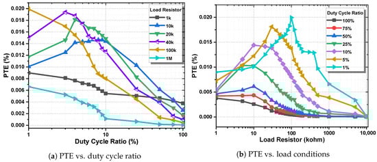
Figure 10.
(a) PTE over the duty cycle ratio for various load resistances. (b) PTE over the load resistance for various duty cycle ratios.
4.3. Optimal Load Conditions
As presented in the previous section, the PTE depends on the load and the duty cycle ratio. The PTE of an inductive link shown in Figure 1 is given by:
where k is the coupling coefficient, and are the quality factors of the TX and RX coils, and and are the equivalent series resistances, which model the losses of the TX and RX coils. , which is connected in parallel to the secondary LC tank, is the AC load resistance that models the rectifier and the load resistor as shown in Figure 11. and are given as follows:
where = /( + ) [39]. In our work, k is very small, so . Equation (7) can be simplified as follows:
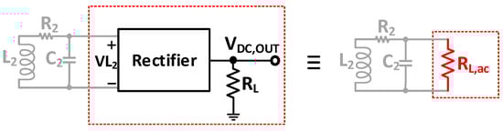
Figure 11.
Illustration for , which is the equivalent parallel resistor for the rectifier and .
To find the maximum condition of the PTE with respect to , we need to take its partial derivative as follows:
Hence, the optimal can be found as follows:
Since typically, Equation (13) can be more simplified to:
Therefore, is the output impedance of the parallel-tuned LC tank on the secondary side (Figure 1).
can be related to the output load () of the rectifier by using the functions of PCE and voltage conversion efficiency (VCE). The PCE is the relationship between the output DC power of the rectifier () and the input power () of the rectifier. The VCE is the relationship between the output DC voltage of the rectifier ( and the input voltage amplitude of the rectifier. The PCE and VCE are given as follows:
where , and . From Equations (14)–(16), the overall optimal load resistance () can be given as follows:
Thus, the optimal load resistance is:
Here, note that PCE and VCE are functions of the rectifier input voltage, which is a function of D.
Using the derived Equation (18), we calculated the optimal load where the proposed WPT system achieves maximum PTE over the duty cycle. Furthermore, we compared the calculated optimal loads with the simulated ones from the results shown in Figure 10b. As shown in Figure 12, the simulated and calculated results are well-matched over the duty cycle.
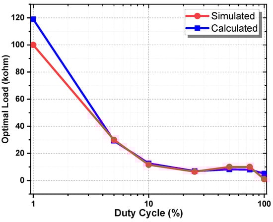
Figure 12.
Simulated and calculated optimized load conditions for the maximum PTE over the duty cycle.
4.4. Practical Constraints
Although the PCE and output DC voltage can be significantly enhanced with the proposed duty-cycled power transmission, there are two practical constraints of the proposed technique: (1) the voltage ripple at and (2) the maximum instantaneous TX power.
Firstly, as the power is transmitted during the active phase only ( in Figure 2), droops during the dormant phase (– in Figure 2), inducing voltage ripples on . The ripple magnitude increases as the duty cycle phase gets shorter for given input power, load condition, and output capacitor.
Figure 13a shows the ripple ratio (RR) in respect to the duty cycle ratio at = 1 s, = 100 k, and = 4 nF. RR is defined as the ratio between the peak-to-peak amplitude of the ripple voltage and the average dc output voltage:
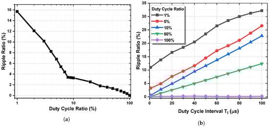
Figure 13.
(a) Ripple ratios (RR) vs. the duty cycle ratio (D) at TI the duty cycle interval of 1 s. (b) RR vs. TI at 100%, 50%, 10%, and 1% of the duty cycle ratios.
As shown in Figure 13a, RR is at the minimum when the power is continuously transmitted (D = 100%). RR increases as D decreases, and it reaches approximately 7% and 15% at D = 5% and 1%, respectively. To further investigate RR, the duty cycle interval is varied from 1 s to 100 s for five fixed duty cycle ratios. As shown in Figure 13b, RR can be decreased by decreasing , while conserving the same duty cycle ratio. It is because the dormant time decreases as decreases even with the same duty cycle ratio.
To reduce the undesirable ripples further, the size of the load capacitor () can be increased. Nevertheless, there is a limit on the size that can be integrated on the semiconductor chip or in the miniaturized millimeter-scale implant. Due to this limit, 4 nF of is chosen as the maximum achievable capacitance and is used in the simulations in this paper. Although RR is high for shorter duty cycle ratios, it can be subdued by high power-supply rejection (PSR) of the low-dropout regulator (LDO) [40,41], which is typically implemented after the rectifier circuit in WPT systems. Moreover, the frequency components of the ripples are typically out of the frequency range of the biological signals of interest. For instance, assume an implant to measure action potentials from neurons. Frequency ranges of the signal and the recording channel are typically from 100 Hz to 10 kHz, so ripples around 1 kHz may affect the signal reading adversely. Such ripples can be avoided easily by choosing outside of the range between 0.1 ms and 10 ms.
In addition to the ripple effect, there are also some instrumental limits in the duty-cycled power transmission. In practice, the instantaneous TX power cannot be increased indefinitely to implement the case for short duty cycle ratios. This is mainly because of limited power supply levels on the TX side. Within a limit of the maximum TX power, the duty cycle ratio can be shortened to increase the effective PDL and PTE.
5. Conclusions
This paper proposed a new system-level duty-cycled WPT technique, which can be applied to miniature biomedical implants. The proposed duty-cycled WPT technique enhances the overall power-transfer efficiency (PTE) to the implants by effectively increasing the power conversion efficiency (PCE) of the rectifier at weak and attenuated input power. Based on an FEM model of a WPT system in HFSS for a 1×1-mm implant on the brain surface, circuit simulations of the proposed method were performed in a 180-nm CMOS SOI process. The proposed technique increases the output voltage and PCE of the rectifier by ×4 and ×4.5, respectively, and hence the overall PTE is improved by ×15, as compared to typical continuous WPT techniques. The proposed technique is more effective for the cases with a low k and a low input voltage for the rectifier. Thus, its potential applications include millimeter-sized implants for brain signal recording and stimulation and other miniature sensors inside the body. This technique can also be applied to wireless power transmission for other environmental sensors that are placed at a low k. In addition, this technique is not limited to the inductively coupled systems only, but it can also be applied to ultrasonic powering. In the future, a fully adaptive input-power-aware duty-cycled WPT system is likely to be proposed. It is expected to be able to decide its duty cycle automatically according to the received power at the implant. Such an adaptive scheme can further optimize the PTE and power delivery under various conditions.
Author Contributions
Conceptualization, K.-W.Y. and S.H.; HFSS modeling, K.-W.Y. and S.H.; Cadence circuit modeling, M.A.A. and K.-W.Y.; simulations, M.A.A. and K.-W.Y.; analysis, M.A.A., K.-W.Y., and S.H.; resources, S.H.; writing—original draft preparation, M.A.A.; writing—review and supervision, S.H. All authors have read and agreed to the published version of the manuscript.
Funding
This research received no external funding.
Conflicts of Interest
The authors declare no conflict of interest.
References
- Khan, S.R.; Pavuluri, S.K.; Cummins, G.; Desmulliez, M.P.Y. Wireless Power Transfer Techniques for Implantable Medical Devices: A Review. Sensors 2020, 20, 3487. [Google Scholar]
- Hui, S.Y.R.; Zhong, W.; Lee, C.K. A Critical Review of Recent Progress in Mid-Range Wireless Power Transfer. IEEE Trans. Power Electron. 2014, 29, 4500–4511. [Google Scholar]
- Wang, W.X.; Dai, H.A. A Critical Review of Wireless Power Transfer via Strongly Coupled Magnetic Resonances. Energies 2014, 7, 4316–4341. [Google Scholar]
- Kim, H.; Hirayama, H.; Kim, S.; Han, K.J.; Zhang, R.; Choi, J. Review of Near-Field Wireless Power and Communication for Biomedical Applications. IEEE Access 2017, 5, 21264–21285. [Google Scholar]
- Basar, M.R.; Ahmad, M.Y.; Ibrahim, F.; Cho, J. Resonant inductive power transfer system for freely moving capsule endoscope with highly uniform magnetic field. In Proceedings of the 2016 IEEE Industrial Electronics and Applications Conference (IEACon), Kota Kinabalu, Malaysia, 20–22 November 2016; pp. 393–397. [Google Scholar]
- Kline, M.; Izyumin, I.; Boser, B.; Sanders, S. Capacitive power transfer for contactless charging. In Proceedings of the 2011 Twenty-Sixth Annual IEEE Applied Power Electronics Conference and Exposition (APEC), Fort Worth, TX, USA, 6–11 March 2011; pp. 1398–1404. [Google Scholar]
- Rahman, M.M.; Adalian, D.; Chang, C.; Scherer, A. Optical power transfer and communication methods for wireless implantable sensing platforms. J. Biomed. Opt. 2015, 20. [Google Scholar] [CrossRef]
- Ozeri, S.; Shmilovitz, D. Ultrasonic transcutaneous energy transfer for powering implanted devices. Ultrasonics 2010, 50, 556–566. [Google Scholar]
- Lu, Y.; Ki, W. CMOS Integrated Circuit Design for Wireless Power Transfer; Springer: New York, NY, USA, 2018; pp. 13–32. [Google Scholar]
- Lee, B.; Jia, Y.; Mirbozorgi, S.A.; Connolly, M.; Tong, X.; Zeng, Z.; Mahmoudi, B.; Ghovanloo, M. An Inductively-Powered Wireless Neural Recording and Stimulation System for Freely-Behaving Animals. IEEE Trans. Biomed. Circuits Syst. 2019, 13, 413–424. [Google Scholar]
- Ahn, D.; Hong, S. Effect of Coupling Between Multiple Transmitters or Multiple Receivers on Wireless Power Transfer. IEEE Trans. Ind. Electron. 2013, 60, 2602–2613. [Google Scholar]
- Yang, K.; Oh, K.; Ha, S. Challenges in Scaling Down of Free-Floating Implantable Neural Interfaces to Millimeter Scale. IEEE Access 2020, 8, 133295–133320. [Google Scholar]
- Feng, P.; Yeon, P.; Cheng, Y.; Ghovanloo, M.; Constandinou, T.G. Chip-Scale Coils for Millimeter-Sized Bio-Implants. IEEE Trans. Biomed. Circuits Syst. 2018, 12, 1088–1099. [Google Scholar]
- Kim, C.; Park, J.; Ha, S.; Akinin, A.; Kubendran, R.; Mercier, P.P.; Cauwenberghs, G. A 3 mm × 3 mm Fully Integrated Wireless Power Receiver and Neural Interface System-on-Chip. IEEE Trans. Biomed. Circuits Syst. 2019, 13, 1736–1746. [Google Scholar] [PubMed]
- Ahn, D.; Ghovanloo, M. Optimal Design of Wireless Power Transmission Links for Millimeter-Sized Biomedical Implants. IEEE Trans. Biomed. Circuits Syst. 2016, 10, 125–137. [Google Scholar] [PubMed]
- Lin, J.C. IEEE Standard for Safety Levels with Respect to Human Exposure to Radio Frequency Electromagnetic Fields, 3 kHz to 300 GHz. IEEE Antennas Propag. Mag. 2006, 48, 157–159. [Google Scholar]
- Jouran, M.A.; Yang, X.; Chen, W. Magnetically coupled resonance WPT: Review of compensation topologies, resonator structures with misalignment, and EMI diagnostics. Electronics 2018, 7, 296. [Google Scholar]
- Hochmair, E.S. System Optimization for Improved Accuracy in Transcutaneous Signal and Power Transmission. IEEE Trans. Biomed. Eng. 1984, 177–186. [Google Scholar] [CrossRef]
- Zierhofer, C.M.; Hochmair, E.S. High-efficiency coupling-insensitive transcutaneous power and data transmission via an inductive link. IEEE Trans. Biomed. Eng. 1990, 37, 716–722. [Google Scholar]
- Mou, Z.; Zheng, X.; Hou, W.; Wang, X.; Wu, X.; Jiang, Y. An Analytical Model for Inductively Coupled Multichannel Implantable System With Micro-Coil Array. IEEE Trans. Magn. 2012, 48, 2421–2429. [Google Scholar]
- Gong, C.; Liu, D.; Miao, Z.; Li, M. A Magnetic-Balanced Inductive Link for the Simultaneous Uplink Data and Power Telemetry. Sensors 2017, 17, 1768. [Google Scholar]
- Jow, U.; Ghovanloo, M. Design and Optimization of Printed Spiral Coils for Efficient Transcutaneous Inductive Power Transmission. IEEE Trans. Biomed. Circuits Syst. 2007, 1, 193–202. [Google Scholar]
- Kiani, M.; Jow, U.; Ghovanloo, M. Design and Optimization of a 3-Coil Inductive Link for Efficient Wireless Power Transmission. IEEE Trans. Biomed. Circuits Syst. 2011, 5, 579–591. [Google Scholar]
- Zargham, M.; Gulak, P.G. Maximum Achievable Efficiency in Near-Field Coupled Power-Transfer Systems. IEEE Trans. Biomed. Circuits Syst. 2012, 6, 228–245. [Google Scholar] [PubMed]
- Kotani, K.; Sasaki, A.; Ito, T. High-Efficiency Differential-Drive CMOS Rectifier for UHF RFIDs. IEEE J. Solid-State Circuits 2009, 44, 3011–3018. [Google Scholar]
- Lee, H.-M.; Ghovanloo, M. An Integrated Power-Efficient Active Rectifier with Offset-Controlled High Speed Comparators for Inductively Powered Applications. IEEE Trans. Circuits Syst. I Regul. Pap. 2011, 58, 1749–1760. [Google Scholar] [PubMed]
- Karimi, Y.; Khalifa, A.; Montlouis, W.; Stanaćević, M.; Etienne-Cummings, R. Coil array design for maximizing wireless power transfer to sub-mm sized implantable devices. In Proceedings of the 2017 IEEE Biomedical Circuits and Systems Conference (BioCAS), Torino, Italy, 19–21 October 2017; pp. 1–4. [Google Scholar]
- Khalifa, A.; Karimi, Y.; Huang, Y.; Stanaćevic, M.; Etienne-Cummings, R. The Challenges of Designing an Inductively Coupled Power Link for μm-sized On-Chip Coils. In Proceedings of the 2018 IEEE Biomedical Circuits and Systems Conference (BioCAS), Cleveland, OH, USA, 17–19 October 2018; pp. 1–4. [Google Scholar]
- Almansouri, A.S.; Ouda, M.H.; Salama, K.N. A CMOS RF-to-DC Power Converter With 86% Efficiency and −19.2-dBm Sensitivity. IEEE Trans. Microw. Theory Tech. 2018, 66, 2409–2415. [Google Scholar]
- Karthaus, U.; Fischer, M. Fully integrated passive UHF RFID transponder IC with 16.7-μW minimum RF input power. IEEE J. Solid-State Circuits 2003, 38, 1602–1608. [Google Scholar]
- Barnett, R.; Balachandran, G.; Lazar, S.; Kramer, B.; Konnail, G.; Rajasekhar, S.; Drobny, V. A Passive UHF RFID Transponder for EPC Gen 2 with −14 dBm Sensitivity in 0.13μm CMOS. In Proceedings of the 2007 IEEE International Solid-State Circuits Conference, San Francisco, CA, USA, 11–15 February 2007; Digest of Technical Papers. pp. 582–623. [Google Scholar]
- Wu, K. Introduction To SCHOTTKY Rectifier and Application Guidelines; Taiwan Semiconductor: Hsinchu, Taiwan, 2003. [Google Scholar]
- Kim, C.; Ha, S.; Park, J.; Akinin, A.; Mercier, P.P.; Cauwenberghs, G. A 144-MHz Fully Integrated Resonant Regulating Rectifier with Hybrid Pulse Modulation for mm-Sized Implants. IEEE J. Solid-State Circuits 2017, 52, 3043–3055. [Google Scholar]
- Xue, Z.; Fan, S.; Li, D.; Zhang, L.; Gou, W.; Geng, L. A 13.56 MHz, 94.1% Peak Efficiency CMOS Active Rectifier with Adaptive Delay Time Control for Wireless Power Transmission Systems. IEEE J. Solid-State Circuits 2019, 54, 1744–1754. [Google Scholar]
- Lee, B.; Ahn, D. Robust Self-Regulated Rectifier for Parallel-Resonant Rx Coil in Multiple-Receiver Wireless Power Transmission System. IEEE J. Emerg. Sel. Top. Power Electron. 2019. [Google Scholar] [CrossRef]
- Lo, C.; Yang, Y.; Tsai, C.; Lee, C.; Yang, C. Novel wireless impulsive power transmission to enhance the conversion efficiency for low input power. In Proceedings of the 2011 IEEE MTT-S International Microwave Workshop Series on Innovative Wireless Power Transmission: Technologies, Systems, and Applications, Kyoto, Japan, 12–13 May 2011; pp. 55–58. [Google Scholar]
- Yang, Y.; Yang, C.; Tsai, C.; Lee, C. Efficiency improvement of the impulsive wireless power transmission through biomedical tissues by varying the duty cycle. In Proceedings of the 2011 IEEE MTT-S International Microwave Workshop Series on Innovative Wireless Power Transmission: Technologies, Systems, and Applications, Kyoto, Japan, 12–13 May 2011; pp. 175–178. [Google Scholar]
- Yang, Y.; Tsai, C.; Yang, C.; Yang, C. Using pulse width and waveform modulation to enhance power conversion efficiency under constraint of low input power. In Proceedings of the 2012 Asia Pacific Microwave Conference Proceedings, Kaohsiung, Taiwan, 4–7 December 2012; pp. 400–402. [Google Scholar]
- Park, J.; Kim, C.; Akinin, A.; Ha, S.; Cauwenberghs, G.; Mercier, P.P. Wireless powering of mm-scale fully-on-chip neural interfaces. In Proceedings of the 2017 IEEE Biomedical Circuits and Systems Conference (BioCAS), Torino, Italy, 19–21 October 2017; pp. 1–4. [Google Scholar]
- Yun, S.J.; Yun, J.S.; Kim, Y.S. Capless LDO Regulator Achieving −76 dB PSR and 96.3 fs FOM. IEEE Trans. Circuits Syst. II Express Briefs 2017, 64, 1147–1151. [Google Scholar]
- Lu, Y.; Ki, W.; Yue, C.P. 17.11 A 0.65 ns-response-time 3.01 ps FOM fully-integrated low-dropout regulator with full-spectrum power-supply-rejection for wideband communication systems. In Proceedings of the 2014 IEEE International Solid-State Circuits Conference Digest of Technical Papers (ISSCC), San Francisco, CA, USA, 9–13 February 2014; pp. 306–307. [Google Scholar]
Publisher’s Note: MDPI stays neutral with regard to jurisdictional claims in published maps and institutional affiliations. |
© 2020 by the authors. Licensee MDPI, Basel, Switzerland. This article is an open access article distributed under the terms and conditions of the Creative Commons Attribution (CC BY) license (http://creativecommons.org/licenses/by/4.0/).