Abstract
In the field of near-infrared weak light detection, an InP/InGaAs single-photon avalanche diode (SPAD) is preferred due to the advantages of high sensitivity, low cost and room-temperature operation. To properly simulate and optimize the SPAD’s front-end circuit, a comprehensive and compact behavior model of the InP/InGaAs SPAD is normally required to accurately describe the statistical behavior of the detectors. In this paper, an InP/InGaAs SPAD analytical model is constructed, which not only includes the direct current (DC) and alternating current (AC) behavior simulating the avalanche and quenching processes, but also describes the dark count, after-pulsing and photon detection efficiency. For dark count noise, three important generation mechanisms are considered, including thermal generation, trap-assisted tunneling and band-to-band tunneling. The model described by the Verilog-A hardware description language (HDL) can be directly implemented in the commercial circuit simulator. A gated mode, passive quenching and recharging circuit is used to simulate and verify the developed model. The simulation results are in good agreement with the reported test data, demonstrating the accuracy of the developed InP/InGaAs SPAD model.
1. Introduction
As an important weak light detection technology, single-photon detection has been widely used in numerous applications, such as high-resolution, three-dimensional (3D) imaging [1], quantum information processing [2], astronomical exploration [3] and spectrum resolution [4]. Particularly, with the rapid development of quantum secure communication technology, long-distance quantum key distribution technology has made a great breakthrough, thus making the single-photon detector working in the infrared band attract more and more attention. Since the InP/InGaAs single-photon avalanche diode (SPAD) has features such as high sensitivity and non-cooling at 1310 nm and 1550 nm, it has become one of the typical detectors in the field of single-photon detection. To achieve high performance, a structure referred to as separate absorption, grading, charge and multiplication (SAGCM) is commonly applied presently [5]. When an InP/InGaAs SPAD with an SAGCM structure operates in Geiger mode, a self-sustaining avalanche current may be triggered by the carriers generated by photon absorption, or other excitation mechanisms, and keeps flowing until the applied voltage across the SPAD is lowered below the breakdown voltage Vbrk. Subsequently, the bias state must be restored to detect the next single photon. Therefore, the front-end electronics, including the quenching and reset circuit and the readout circuit, are required for successive single-photon detection [6]. To properly simulate and optimize the overall performance of the front-end circuit, a compact and accurate model for an InP/InGaAs SPAD operating in the commercial circuit simulator is urgently needed.
Up to now, the circuit model for Si-based SPADs has been successfully developed. For example, an accurate Si-based SPAD circuit model, including the important generation mechanisms of the statistical behaviors, was proposed in [7], and key device parameters, such as the avalanche triggering probability and electric field profile, were extracted from the Geiger-mode TCAD simulation to improve the model’s accuracy. Different to the typical Si-based SPAD, whose absorption and multiplication processes all occur in the depletion region of the p–n junction, the InP/InGaAs SPAD usually separates the absorption and multiplication regions to obtain optimal device performance. As a result, the generation mechanisms and contributions of dark carriers are apparently different from that of Si-based SPADs. To obtain optimal device performance, many theoretical models have been established to analyze the characteristics of InGaAs/InP SPADs. For example, Donnelly et al. [8] presented an experimental model to predict the dark count rate (DCR) and photon detection efficiency (PDE), but after-pulsing was not considered. Subsequently, [9] supplemented the after-pulsing, but the temperature effect of the carrier lifetime related to the Shockley–Read–Hall (SRH) model was ignored. Additionally, Mofasser et al. [10] proposed a semi-numerical iterative model to calculate the photo current and the dark count probability, but the iterative procedure increased computational complexity. Moreover, the location dependence of the triggering probability was not included. Although great progress has been achieved in the field of the theoretical model, there are few reports on the InP/InGaAs SPAD circuit model for the cooperative design of the SPAD and the front-end circuit. Recently, a PIN InP/InGaAs SPAD model was constructed [11] based on the Si-based circuit model proposed by Dalla Mora [12], but the DCR and after-pulsing were not considered in that model.
Based on the previous modeling work [13,14,15,16] and the operating principle of InP/InGaAs SAGCM SPADs, a compact and accurate circuit simulation model was established. This model not only describes the static and dynamic behavior, but also includes the noise statistical behavior and PDE. Most importantly, both the absorption region and the multiplication region are taken into account, and the temperature dependence of the carrier lifetime related to the SRH process is considered. Furthermore, the triggering probability of different positions in the multiplication region is calculated, and the expression is simplified through curve fitting, which is convenient to embed in our developed circuit model. As a result, this model implemented in the Verilog-A HDL is compatible with a commercial circuit simulator. The simulation results in gated mode fit well with the measured data, validating the accuracy of the proposed model.
2. Structure and Principle of an InP/InGaAs SPAD
Figure 1 illustrates a two-dimensional (2D) schematic of the InP/InGaAs SAGCM SPAD used in the work. The n+-InP buffer layer, serving as the n-side of the junction, was grown on the n+-InP substrate, and an undoped InGaAs absorption layer with band gap energy of 0.75 eV was deposited. Then, a large band gap InP layer (1.35 eV) was adopted as the multiplication region to suppress the tunneling current in the avalanche multiplication process. To buffer the abrupt change of the band gap between the InGaAs and InP and eliminate the accumulation effect of photo-generated carriers at the interface, an InGaAsP grading layer was added. Additionally, a charge layer adjacent to the grading layer was used to flexibly adjust the electric field profile of the InP/InGaAs SPAD. After the epitaxial growth, two-step p-type zinc diffusion was introduced to confine the high field in the active area and avoid the premature edge breakdown.
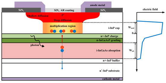
Figure 1.
Two-dimensional (2D) schematic of the InP/InGaAs single-photon avalanche diode (SPAD). The electric field profile is shown on the right.
When incident photons were absorbed in the InGaAs layer of an SPAD operating in Geiger mode, the photo-induced electrons were captured by the cathode, and the holes drifted through the charge layer and were injected into the multiplication region. Subsequently, avalanche events happened by a chain collision with the InP lattice under the acceleration of a high electric field. In the absence of photons, dark carriers generated in different regions may have drifted into the multiplication region, thus triggering avalanche events and causing false counts. Although there are many dark carrier generation mechanisms in an InP/InGaAs SPAD, the dominant contributions to the DCR [17] are as follows: (1) generation–recombination in the depletion region; (2) band-to-band tunneling (BTBT); and (3) trap-assisted tunneling (TAT). Since the thicknesses of the grading and the charge layers were much smaller than those of the absorption and the multiplication regions, the dark count in these two layers was neglected for simplicity.
When the avalanche was triggered by photons or dark carriers, the generated carriers may have been trapped by the deep-level traps and subsequently released after a delayed amount of time.
If the SPAD was biased above its breakdown voltage Vbrk at this moment, an after-pulsing event may have been induced which contributed to the secondary dark counts [18].
3. SPAD Analytical Model
Based on the previous modeling works [13,14,15,16,17] and the operating principle described in Section 2, a modified analytical model of an InP/InGaAs SPAD under a reversed biasing condition was developed, as shown in Figure 2.
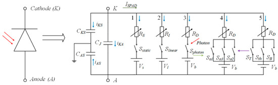
Figure 2.
Analytical model of an InP/InGaAs SPAD.
Five different DC paths were presented to emulate the operating process of an InP/InGaAs SPAD. In each path, a voltage-controlled switch SX, a nonlinear breakdown resistance RX and a DC voltage generator VX, where X represented different working regions, were adopted to accurately reconstruct the measured I–V curves.
The first and the second paths simulated the static and linear operating region, respectively, where the SPAD was reversely biased under Vbrk. The third path was used to emulate the Geiger mode triggered by incident photons. The fifth path mimicked the avalanche triggering caused by the dark carriers generated by thermal generation, TAT and BTBT, respectively. The last path represented the generation of after-pulsing, where three-type traps illustrated by switches were assumed according to the theoretical analysis of experimental results [19]. Since the carriers generated by photons or dark carriers might be captured by the traps, the switches in the fourth path were determined by the third and fifth paths. The total DC generated by these paths was denoted as ISPAD, and the AC behavior was modeled by three capacitors marked as CJ, CKS and CAS. Here, CJ is a voltage-dependent junction capacitance, and CKS and CAS are the cathode-to-substrate and anode-to-substrate stray capacitors, respectively.
3.1. Basic Behavior Modeling
As mentioned above, the DC behavior was reconstructed by using a nonlinear SPAD resistor RX,i, derived from the piecewise linear I–V modeling under the condition of reversed biasing [13]. To avoid the convergence problem at the joints of curves, a fully differentiable pseudo-min-max function was introduced, and the DC avalanche current flowing through the SPAD is given by [13]
where, IX,i and VX,i represent the corresponding current and voltage, respectively, of the ith selected point in X region and Vn is a normalization voltage of about 10 mV.
The dynamic behavior of the SPAD was determined by the charges stored in the depletion region and the stray capacitors. The two stray capacitors, CkS and CAS, depended on the structural dimensions and packaging in practical applications, but they were regarded as constants here to simplify the modeling. The charges stored in CJ, CKS and CAS can be expressed respectively with [20]
where A is the effective area, Vbi is the built-in voltage, mj is the junction grading coefficient whose value is 0.5, VKA is the applied voltage across the SPAD and CJ0 is the zero-voltage junction capacitance per unit area. VK and VA are the voltages of the cathode and anode with respect to the substrate. Based on Kirchhoff’s current law, the total cathode and anode currents are given by
3.2. Dark Count Modeling
As the primary noise source of the SPAD, the dark count strongly depends on temperature and excess voltage. For a well-designed InP/InGaAs SPAD, the dark carriers generated in the absorption and multiplication regions are the main causes of the dark count. For the absorption region, the electrons from the valence band can be elevated into the conduction band due to thermal activation, thus generating intrinsic carriers. If these carriers move to the multiplication region, they may trigger false avalanche events when the SPAD is biased above its Vbrk. Since the electric field in the InGaAs absorption region is normally much lower than that in the multiplication region, by adjusting the charge regions, as shown in Figure 1, the tunneling effect in this region is negligible.
As the multiplication region undergoes a high electric field, the dark carriers generated by TAT and BTBT dominate in the InP multiplication region, and the contribution of thermal generation to the dark count in this region can be ignored due to the large band gap of InP [21].
Additionally, experimental results showed that the dark current related to surface recombination only leaked through the low electric field periphery [22] and did not succeed in triggering avalanche events, so the influence of dark current carriers was not considered here.
For a well-designed InP/InGaAs SPAD, the InGaAsP grading region eliminates the hole accumulation between the InGaAs absorption region and the InP multiplication region. Thus, most of the holes generated in the absorption region will drift to the multiplication region. In this work, the hole transport efficiency from the absorption region to the multiplication region was assumed to be one, and no multiplication occurred in the absorption region due to the low electric field in this region.
Usually, SRH theory is used to determine the carrier thermal generation rate. As described in Figure 1, the InGaAs absorption region was undoped, so the electron and hole concentrations were much lower than the intrinsic carrier concentration ni. In such a case, the carrier thermal generation rate in the InGaAs absorption region can be simply expressed as [13]
where τe and τh represent the electron and hole lifetimes, respectively, Ei is the intrinsic Fermi level, Et is the trap level, k is the Boltzmann constant, T is the absolute temperature and Wab is the absorption region thickness.
For the multiplication region in Geiger mode, the electric field was so high that local band bending may have been sufficient to allow electrons to tunnel from the valence band into the conduction band. In this case, the contribution of carriers generated by the BTBT process should be considered, and the corresponding generation rate of dark carriers is defined as [9]
where q is the electric charge, mr is the reduced mass of the conduction band’s effective mass mc and the light hole’s effective mass mlh, ħ is the reduced Planck constant, F is a position-dependent electric field that varies with the excess voltage and Wmul is the multiplication region thickness.
Since there may be some defects in the InP multiplication region due to epitaxial growth or fabrication processing, the TAT mechanism may have had a strong impact on the occurrence of dark counts. The generation rate of dark carriers caused by TAT can be expressed as [9]
where the barrier heights EB1 and EB2 govern tunneling from the valence band to the trap and the trap to the conduction band, respectively, and the parameters are set as EB1 = 0.75EInP and EB2 = 0.25EInP. Nv,InP and Nc,InP are the effective state densities for the valence and the conduction bands, respectively, and Ntrap is the trap concentration.
The avalanche triggering probability is an important parameter in the numerical calculation of statistical performance, and relates to the positions of the carriers [23]. In this work, an empirical equation described in [11,13,23] is used:
where ηT is exponential slope at a given temperature and Vex is the excess voltage.
Following the derivation of the avalanche triggering probability described by Oldham [24], the theoretical triggering probability PA(x) at position (x) in the multiplication region could be calculated. At a certain temperature, the avalanche triggering probabilities at a fixed position under different excess voltages were fitted using Equation (10), and the position-dependent triggering probabilities PA(x) could be calculated successively. Then, the exponential slopes ηT at different positions were extracted from equations and fitted to ηT(x). For example, ηT(x) at 225 K can be expressed as
As a result, the triggering probabilities of photo-generated carriers and dark carriers generated in the absorption region were considered to be PA(0), where x = 0 corresponded to the beginning of the multiplication region [8]. To simplify the calculation, the triggering probability in the multiplication region was supposed to be the probability of the center of the region PA(Wmul/2) [7].
Based on the above analyses, the total DCR in the absorption and the multiplication regions can be calculated by
3.3. Photon Detection Efficiency Modeling
Due to the small thicknesses of the grading and charge regions, as well as the wide band gap of InP multiplication, the photon absorption in these regions could be ignored [25]. Thus, the photon detection efficiency of the SPAD is expressed as
where, R is the surface reflectivity, Pab is the absorption efficiency (which is modeled by Pab = 1 − exp(−αab·Wab) [8] and αab is the absorption coefficient of the InGaAs material and can be obtained in [26]. As discussed in Section 3.2, the transport efficiency of a photo-generated hole from the absorption region to the multiplication region was assumed to be one in this paper.
3.4. After-Pulsing Behavior
As described above, there were many deep-level traps in the SPAD epitaxial structure. The lifetime of each energy level can be expressed by [21]
where Eai is the activation energy and τ0i is the ith pre-exponential factor. The trap’s lifetime decreased with the increasing temperature.
Additionally, the after-pulsing probability also depended on time. If the time interval between the avalanche and the release of trapped carriers was very small, the released carriers had high avalanche triggering probabilities. Therefore, the after-pulsing probability can be expressed as follows [18]:
where Ai is the correction factor of the ith level and t is the delay from an avalanche.
In this model, the after-pulsing parameters of the InP/InGaAs SPAD were exacted from [27], and three-type deep-level traps in the band gap were obtained by a fitting method described in [13].
3.5. Consideration of Temperature Dependence
To suppress the dark count noise, an InP/InGaAs SPAD often operates at a low temperature in practical applications, so it is necessary to consider the temperature dependence of key parameters. In this model, the primary parameters, including the InGaAs intrinsic carrier concentration ni,InGaAs, the band gap energies of InGaAs and InP and the SPAD breakdown voltage Vbrk, can be calculated by the following equations [28,29]:
where NC,InGaAs and NV,InGaAs are the effective state densities in the conduction band and valence band, respectively, Eg0,InGaAs is the band gap energy of InGaAs at 4.5 K, Eg0,InP is the band gap energy of InP at 1.5 K, a1, a2, b1 and b2 are the temperature coefficients of the band gap energy, Vbrk0 is the breakdown voltage at room temperature T0 and γ is the temperature coefficient of the breakdown voltage.
4. Verilog-A HDL Implementation
The circuit model of the InP/InGaAs SPAD was implemented in the Verilog-A hardware description language (HDL), and a state transition diagram similar to [13] is shown in Figure 3. The operating procedure can be described as follows. Firstly, the physical parameters and internal signals are initialized, and the model is set to Geiger mode. When a photon is an incident photon, there will be an avalanche triggering probability PA. If PA is larger than the threshold probability Pth, the avalanche will be triggered, and the dark count timer and after-pulsing timer are updated simultaneously. If PA is smaller than Pth, it returns to Geiger mode for the next judgment. If there is no incident photon when the simulation time reaches the set value, the dark count timer or after-pulsing timer will be triggered and execute the judgment of event occurrence; the judgment mechanisms are similar to that of the photon trigger. If the dark count events or after-pulsing events occur, the internal signal and the timers will be updated to mark the occurrence time of the next event. When the event ends, the model is set to the state of below breakdown to start the next round of avalanche judgment.
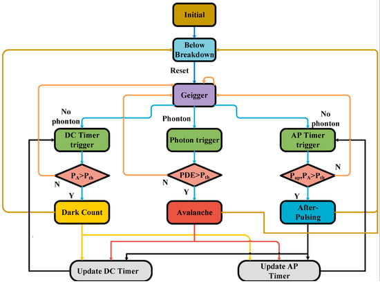
Figure 3.
State transition diagram of a Geiger model.
The key parameters used in the InP/InGaAs SPAD model are summarized in Table 1. The values of the active area, layer thickness, after-pulsing parameter and Vbreak0 are from [27]. The values of stray capacitances are from [30], and other values were obtained by simulation fitting.

Table 1.
Summary of key parameters.
5. Simulation and Verification
The SPAD is described as a three-terminal module. A and K stand for the anode and cathode, respectively, and P is used to emulate the photon arrival. A gated mode, passive quenching-and-recharging circuit (PQRC), as shown in Figure 4a, was used to validate the accuracy of the developed SPAD model. A 10 ps narrow pulse was used to simulate the incident photon. A DC voltage source Vdc of 58 V was applied to provide a basic bias, and a 7 V pulse voltage Vgate coupled through a capacitor Cg (10 nF) was superposed on the Vdc to make the SPAD avalanche. The values of the load resistor RL and the sense resistor RS were 50 Ω and 10 MΩ, respectively. In the following simulations, the gate-ON time was fixed at 20 ns, and the gate-OFF time varied between 1 µs and 100 µs.
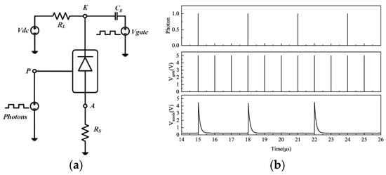
Figure 4.
(a) A passive quenching-and-recharging circuit (PQRC) applied in an SPAD model simulation. (b) An SPAD transient simulation.
Figure 4b illustrates an example of transient simulation waveforms at 225 K with an excess voltage of 5 V and a gate-OFF time of 1 µs. Two avalanche events caused by photons were detected at 15 µs and 18 µs, and then a dark noise (dark count or after-pulsing) was observed at 22 µs.
To analyze the statistical behavior of the dark count at low temperatures, the P port of the SPAD was connected to the ground during the simulation. Figure 5 shows the simulated primary dark count’s dependence of excess voltage at 225 K, with a gate-OFF time of 100 µs to rule out after-pulsing. For comparison, the experimental data reported in [27] are given too. The simulation DCR had good agreement with the experimental data at various excess voltages, and a maximum relative error of 11.2% happened at 3 V of excess voltage. It is clear that the contribution of TAT in the multiplication region dominated for the InP/InGaAs SPAD at 225 K. This was apparently different to the dark noise of the Si-based SPAD, where BTBT contributed the main component of the DCR at low temperatures [13]. Compared with TAT, the contributions of BTBT and thermal generation could be ignored at low temperatures.
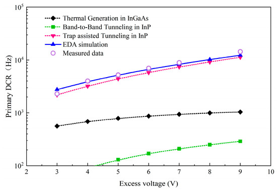
Figure 5.
Simulation results of the voltage dependence of the primary dark count rate (DCR) (T = 225 K).
Figure 6 shows the simulated primary DCR as a function of the temperature with an excess voltage of 5 V. As expected, TAT and BTBT were less temperature dependent than thermal generation. Thermal generation dominated at high temperatures, but TAT was the main source of dark counts when the temperature decreased below 245 K.
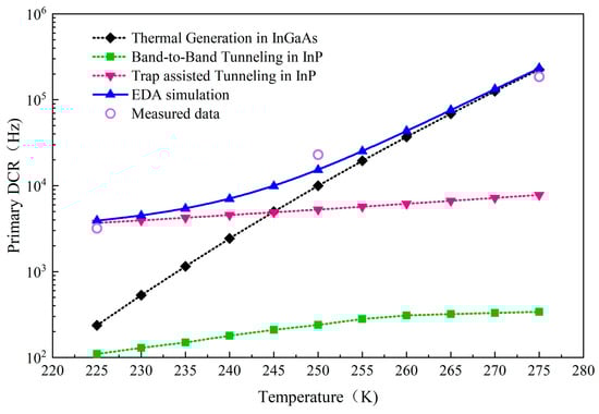
Figure 6.
Simulation results of the temperature dependence of the primary DCR (Vex = 5 V).
Figure 7 shows the simulated total DCR variation with the gate-OFF time (which corresponds to the dead time) at 225 K. Although there is a little gap at the long gate-OFF time, the simulation and the measured results are in reasonable agreement. When a short gate-OFF time was set, the total DCR increased because of after-pulsing. The after-pulsing was apparently visible at a higher excess bias when the gate-OFF time was smaller than 10 μs, and it could be obtained by subtracting the primary dark counts from the total DCR. The shadow areas in the figure show the contribution of after-pulsing to the total DCR.
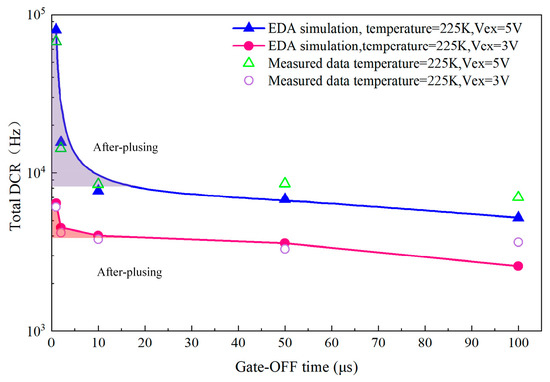
Figure 7.
The variety of the total DCR with gate-OFF times.
As expected, the after-pulsing decreased exponentially with the increased gate-OFF time, which is in accordance with the description of Equation (15). Additionally, a small excess voltage was beneficial for improving the after-pulsing.
To apply the developed InP/InGaAs SPAD model to different working conditions, the DCR was predicted under different temperatures and excess voltages, as shown in Figure 8. As can be seen in the figure, a low operating temperature and a small excess voltage were good for improving the dark noise, but they would deteriorate the photon detection efficiency. By comparing the trends in Figure 8a,b, it can be seen that the DCR’s temperature dependence was stronger than its excess voltage dependence. Therefore, an InP/InGaAs SPAD operating at a low temperature is preferred in practical applications.
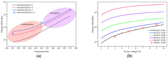
Figure 8.
(a) Simulation results of the primary DCR with temperatures at three different excess voltages. (b) Simulation results of the primary DCR with excess voltages at five different temperatures.
As the excess voltage increased, the PDE at 1550 nm improved thanks to the higher avalanche probability. Unfortunately, the primary DCR also increased because of the electric field-related impact ionization coefficients and the tunneling mechanism. Thus, the SPAD needed a trade-off between the DCR and the PDE. Figure 9 shows the relationship between the primary DCR and PDE at different operating temperatures. As shown in the figure, the simulation results accorded well with the experimental data [27], and a maximum error of 5.3% happened at 3 V of excess voltage. Since a low DCR and a high PDE could be obtained at low temperature, a low temperature was preferred for the InP/InGaAs SPAD.
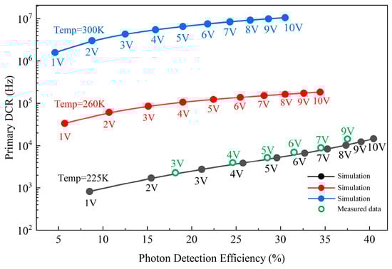
Figure 9.
The relationship between the DCR and the photon detection efficiency (PDE).
To quantify the sensitivity of the SPAD, the noise equivalent power (NEP) is commonly used and can be calculated from the following equation [31]:
where h is the Planck constant and ν is the frequency of the incident radiation.
Figure 10 shows the dependence of the NEP on the excess voltage for the SPAD. At 225 K and a lower voltage, the NEP increased with the decreasing excess voltage due to the reduction of the PDE, but it increased with the increasing excess voltage at higher voltages. This was because the dependence of the DCR on the electric field was stronger than that of the PDE. An optimal excess voltage was located at around 4 V. When the SPAD operated at a higher temperature, due to the DCR being dominated by the thermal generation, the NEP always decreased with the increasing excess voltage. The simulated NEP was close to the data reported in [32].
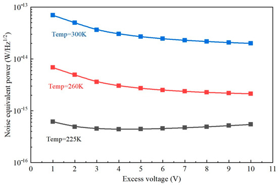
Figure 10.
The dependence of the noise equivalent power (NEP) on the excess voltage.
6. Conclusions
In this paper, a comprehensive circuit model for an InP/InGaAs SPAD was developed to precisely describe the noise statistical performance and photon detection efficiency. In this model, three main generation mechanisms, including SRH recombination in the absorption region, BTBT and TAT in the multiplication region, were taken into account to simulate dark count events. The after-pulsing was characterized by three-type traps, whose lifetime was temperature-dependent and triggering probability was the temporal dependent. The developed model was implemented in Verilog-A HDL, and the simulations were successfully performed in Cadence Spectre, thus showing good compatibility. The simulation results accorded with the tested data, validating the feasibility of the model. Furthermore, the primary DCRs, PDE, and NEP under different excess voltages and temperatures were predicted to evaluate the SPAD performance. The work described here is very suitable to perform SPAD front-end circuit simulation and optimization with good universality and compatibility. Timing jitter, an important statistical feature, was not taken into account in this work, but the circuit model can be applied in many scenarios. For example, in photon-counting imaging, the performance of the SPAD detector can be evaluated in a simulation, since imaging quality is mainly limited by the dark noise rather than by timing jitter.
Author Contributions
Conceptualization, S.X. and J.L.; methodology, S.X. and J.L.; software, S.X. and J.L.; validation, S.X., J.L. and F.Z.; formal analysis, S.X.; investigation, S.X. and J.L.; resources, S.X., J.L. and F.Z.; data curation, S.X.; writing—original draft preparation, S.X.; writing—review and editing, S.X., J.L. and F.Z.; project administration, S.X.; funding acquisition, S.X. All authors have read and agreed to the published version of the manuscript.
Funding
This work was funded by the National Natural Science Foundation of China (No. 11673019).
Conflicts of Interest
The authors declare no conflict of interest.
References
- Castello, M.; Tortarolo, G.; Buttafava, M.; Deguchi, T.; Villa, F.; Koho, S.; Pesce, L.; Oneto, M.; Pelicci, S.; Lanzano, L.; et al. A robust and versatile platform for image scanning microscopy enabling super-resolution FLIM. Nat. Methods 2019, 16, 175. [Google Scholar] [CrossRef] [PubMed]
- Zimmermann, H.; Steindl, B.; Hofbauer, M.; Enne, R. Integrated fiber optical receiver reducing the gap to the quantum limit. Sci. Rep. 2017, 7, 12. [Google Scholar] [CrossRef] [PubMed]
- Ziarkash, A.W.; Joshi, S.K.; Stipcevic, M.; Ursin, R. Comparative study of afterpulsing behavior and models in single photon counting avalanche photo diode detectors. Sci. Rep. 2018, 8, 5076. [Google Scholar] [CrossRef] [PubMed]
- Zhang, H.; Liu, J.; Guo, J.; Xiao, L.; Xie, J. Photon energy-dependent timing jitter and spectrum resolution research based on time-resolved SNSPDs. Opt. Express 2020, 28, 16696–16707. [Google Scholar] [CrossRef]
- Chen, J.; Zhang, Z.; Zhu, M.; Xu, J.; Li, X. Optimization of InGaAs/InAlAs Avalanche Photodiodes. Nanoscale Res. Lett. 2017, 12, 33. [Google Scholar] [CrossRef]
- Straka, I.; Grygar, J.; Hlousek, J.; Jezek, M. Counting Statistics of Actively Quenched SPADs under Continuous Illumination. J. Lightwave Technol. 2020, 38, 4765–4771. [Google Scholar] [CrossRef]
- Xu, Y.; Zhao, T.; Li, D. An accurate behavioral model for single-photon avalanche diode statistical performance simulation. Superlattices Microstruct. 2018, 113, 635–643. [Google Scholar] [CrossRef]
- Donnelly, J.P.; Duerr, E.K.; McIntosh, K.A.; Dauler, E.A.; Oakley, D.C.; Groves, S.H.; Vineis, C.J.; Mahoney, L.J.; Molvar, K.M.; Hopman, P.I.; et al. Design considerations for 1.06-μm InGaAsP-InP Geiger-mode avalanche photodiodes. IEEE J. Quantum Electron. 2006, 42, 797–809. [Google Scholar] [CrossRef]
- Jiang, X.; Itzler, M.A.; Ben-Michael, R.; Slomkowski, K. InGaAsP-InP avalanche photodiodes for single photon detection. IEEE J. Sel. Top. Quantum Electron. 2007, 13, 895–905. [Google Scholar] [CrossRef]
- Mofasser, A.; Saha, S.; Hadi, K.S.; Mohammedy, F.M.; El-Batawy, Y. Modeling of Photocurrent and Dark Count Probability of InGaAs/InP Single Photon Avalanche Photodiode. In Proceedings of the IEEE International Conference on Telecommunications and Photonics (ICTP), Dhaka, Bangladesh, 26–28 December 2017; pp. 147–151. [Google Scholar]
- Zheng, L.; Tian, J.; Weng, Z.; Hu, H.; Wu, J.; Sun, W. An Improved Convergent Model for Single-Photon Avalanche Diodes. IEEE Photonics Technol. Lett. 2017, 29, 798–801. [Google Scholar] [CrossRef]
- Dalla Mora, A.; Tosi, A.; Tisa, S.; Zappa, F. Single-photon avalanche diode model for circuit simulations. IEEE Photonics Technol. Lett. 2007, 19, 1922–1924. [Google Scholar] [CrossRef]
- Cheng, Z.; Zheng, X.; Palubiak, D.; Deen, M.J.; Peng, H. A Comprehensive and Accurate Analytical SPAD Model for Circuit Simulation. IEEE Trans. Electron Devices 2016, 63, 1940–1948. [Google Scholar] [CrossRef]
- Fregonese, S.; Venica, S.; Driussi, F.; Zimmer, T. Electrical Compact Modeling of Graphene Base Transistors. Electronics 2015, 4, 969–978. [Google Scholar] [CrossRef]
- Rodriguez, R.; Gonzalez, B.; Garcia, J.; Toulon, G.; Morancho, F.; Nunez, A. DC Gate Leakage Current Model Accounting for Trapping Effects in AlGaN/GaN HEMTs. Electronics 2018, 7, 210. [Google Scholar] [CrossRef]
- Petticrew, J.D.; Dimler, S.J.; Tan, C.H.; Ng, J.S. Modeling Temperature Dependent Avalanche Characteristics of InP. J. Lightwave Technol. 2020, 38, 4183. [Google Scholar] [CrossRef]
- Karve, G.V. Avalanche Photodiodes as Single Photon Detectors; The University of Texas at Austin: Austin, TX, USA, 2005. [Google Scholar]
- Itzler, M.A.; Jiang, X.; Entwistle, M. Power law temporal dependence of InGaAs/InP SPAD afterpulsing. J. Mod. Opt. 2012, 59, 1472–1480. [Google Scholar] [CrossRef]
- Anti, M.; Tosi, A.; Acerbi, F.; Zappa, F. Modeling of afterpulsing in Single-Photon Avalanche Diodes. In Proceedings of the SPIE Physics and Simulation of Optoelectronic Devices XIX, San Francisco, CA, USA, 24–27 January 2011; Volume 7933. [Google Scholar]
- Giustolisi, G.; Mita, R.; Palumbo, G. Verilog—A modeling of SPAD statistical phenomena. In Proceedings of the 2011 IEEE International Symposium of Circuits an Systems (ISCAS), Rio de Janeiro, Brazil, 15–18 May 2011; pp. 773–776. [Google Scholar]
- Jensen, K.E.; Hopman, P.I.; Duerr, E.K.; Dauler, E.A.; Donnelly, J.P.; Groves, S.H.; Mahoney, L.J.; McIntosh, K.A.; Molvar, K.M.; Napoleone, A.; et al. Afterpulsing in Geiger-mode avalanche photodiodes for 1.06 μm wavelength. Appl. Phys. Lett. 2006, 88, 133503. [Google Scholar] [CrossRef]
- Karve, G.; Wang, S.; Ma, F.; Li, X.; Campbell, J.C.; Ispasoiu, R.G.; Bethune, D.S.; Risk, W.P.; Kinsey, G.S.; Boisvert, J.C.; et al. Origin of dark counts in In0.53Ga0.47As/In0.52Al0.48As avalanche photodiodes operated in Geiger mode. Appl. Phys. Lett. 2005, 86, 063505. [Google Scholar] [CrossRef]
- Itzler, M.A.; Ben-Michael, R.; Hsu, C.F.; Slomkowski, K.; Tosi, A.; Cova, S.; Zappa, F.; Ispasoiu, R. Single photon avalanche diodes (SPADs) for 1.5 μm photon counting applications. J. Mod. Opt. 2007, 54, 283–304. [Google Scholar] [CrossRef]
- Oldham, W.G.; Samuelson, R.R.; Antognetti, P. Triggering phenomena in avalanche diodes. IEEE Trans. Electron Devices 1972, 19, 1056–1060. [Google Scholar] [CrossRef]
- Acerbi, F.; Anti, M.; Tosi, A.; Zappa, F. Design Criteria for InGaAs/InP Single-Photon Avalanche Diode. IEEE Photonics J. 2013, 5, 6800209. [Google Scholar] [CrossRef]
- Adachi, S. Optical dispersion relations for GaP, GaAs, GaSb, InP, InAs, InSb, Alx Ga1−xAs, and In1−xGaxAsyP1−y. J. Appl. Phys. 1989, 66, 6030–6040. [Google Scholar] [CrossRef]
- Tosi, A.; Calandri, N.; Sanzaro, M.; Acerbi, F. Low-Noise, Low-Jitter, High Detection Efficiency InGaAs/InP Single-Photon Avalanche Diode. IEEE J. Sel. Top. Quantum Electron. 2014, 20, 192–197. [Google Scholar] [CrossRef]
- Hang, Z.; Shen, H.; Pollak, F.H. Temperature dependence of the Eo and Eo + △o gaps of InP up to 600 °C. Solid State Commun. 1990, 73, 15–18. [Google Scholar] [CrossRef]
- Yu, P.W.; Kuphal, E. Photoluminescence of Mn- and Un-doped Ga0.47In0.53As on InP. Solid State Commun. 1984, 49, 907–910. [Google Scholar] [CrossRef]
- Huang, D.; Zhu, R.; Liu, S.; Sun, W.; Wu, J.; Ma, D. SPICE Modeling for Single Photon Avalanche Diode. In Proceedings of the SPIE 5th International Symposium on Photoelectronic Detection and Imaging (ISPDI)-Imaging Sensors and Applications, Beijing, China, 25–27 June 2013; Volume 8908. [Google Scholar]
- Soref, R.A.; De Leonardis, F.; Passaro, V.M.N. Simulations of Nanoscale Room Temperature Waveguide-Coupled Single-Photon Avalanche Detectors for Silicon Photonic Sensing and Quantum Applications. ACS Appl. Nano Mater. 2019, 2, 7503–7512. [Google Scholar] [CrossRef]
- Bai, P.; Zhang, Y.H.; Shen, W.Z. Infrared single photon detector based on optical up-converter at 1550 nm. Sci. Rep. 2017, 7, 15341. [Google Scholar] [CrossRef] [PubMed]
Publisher’s Note: MDPI stays neutral with regard to jurisdictional claims in published maps and institutional affiliations. |
© 2020 by the authors. Licensee MDPI, Basel, Switzerland. This article is an open access article distributed under the terms and conditions of the Creative Commons Attribution (CC BY) license (http://creativecommons.org/licenses/by/4.0/).