Article

Switchable DBR Filters Using Semiconductor Distributed Doped Areas (ScDDAs)

1
Laboratoire des Sciences et Techniques de l’Information, de la Communication et de la Connaissance (Lab-STICC), UMR CNRS 6285, University of Brest, 29238 Brest, France
2
Laboratory of the GREMAN (Groupe de Recherche En Matériaux, Microélectronique, Acoustique et Nanotechnologies), UMR CNRS 7347, University of Tours, 37071 Tours, France
*
Author to whom correspondence should be addressed.
Electronics 2020, 9(12), 2021; https://doi.org/10.3390/electronics9122021
Submission received: 3 November 2020 / Revised: 19 November 2020 / Accepted: 26 November 2020 / Published: 30 November 2020

Abstract

:
This paper presents a novel way to switch dual-behavior resonator (DBR) filters without any additional active surface-mount components. By using a semiconductor substrate, we were able to simultaneously co-design the filters and semiconductor distributed doped areas (ScDDAs) with integrated N+PP+ junctions as active elements. These ScDDAs act as electrical vias in the substrate, which makes it possible to have an open-circuited resonator in the OFF state and a short-circuited resonator in the ON state, and, consequently, to control the transmission zeroes of the filters. This method offers degrees of freedom as the dimensions and positions of these doped areas can be chosen to obtain the best performances. In this study, four filters were simulated and fabricated to spotlight different possibilities for the dimensions and positions of the ScDDA to control the low- or high-frequency transmission zero of the filters. The simulations were in very good agreement with the measured results. All the filters present insertion losses lower than 2 dB in the OFF and ON states, a great flexibility in the frequency choice, and good agility compared with the state of the art.

1. Introduction

In the era of the Internet of Things and Internet of Everything, communication systems are omnipresent. It has never been as complicated as it is today, therefore, to obtain satisfactory tradeoffs between electrical and thermal performances, integrability, and cost. A system has to support increasing numbers of applications and its components such as antennas or filters consequently need reconfigurable functionalities. Filters have to select each desired frequency band related to the targeted applications. There exist many discrete reconfigurable filters making it possible to switch a filter from bandpass to bandstop [1,2,3,4], between different bandwidths [5,6,7] or between different frequency bands, sometimes with multi-states, i.e., with a combination of states of several active elements [8,9,10,11,12,13,14,15,16]. However, if active surface-mount components (SMCs) such as PIN diodes, RF MEMS or varactor diodes are used to effect such changes, the filters can have issues related to parasitic effects induced by these active components and their associated bias networks. Whole filter performances may thus be decreased by these parasitic effects, which are potentially exacerbated as the frequency increases.
Moreover, while the frequency spectrum becomes increasingly congested, basing filters on dual-behavior resonators (DBR) can provide narrow-band filters [17,18]. Previous studies have shown the interest of making these components tunable [19,20,21,22] by using additional lines at the end of each stub, PIN diodes, varactors, or KTN ferroelectric thin-films in order to reach a center frequency agility of up to 32%. However, drawbacks have been reported, like a high control voltage, dependence of the transmission zeroes, and occasional high losses caused by the active SMCs.
In order to counter these issues, reconfigurable RF components can be co-designed using semiconductor distributed doped areas (ScDDAs), such as in [23,24,25,26,27]. By designing a tunable RF device with ScDDAs, we can obtain a tunability comparable to that of classical technology with SMCs while avoiding the need for other components. Indeed, ScDDAs are semiconductor junctions acting as electrical vias in the substrate thickness, i.e., they are integrated active components in the substrate. This method offers flexibility in terms of dimensions and positions of the active elements and avoids the drawbacks of adding SMCs.
In this context, the aim of the present paper is to propose narrow-band filters such as DBR ones using ScDDAs. This offers filter designers more possibilities for the control of the frequency zeroes and means to achieve good tradeoffs in terms of electrical performances, integrability, and cost.
In this paper, Section 2 deals with the switchable DBR concept. Then, Section 3 explains the co-simulation method and the measured results on a first demonstrator. Finally, in Section 4, the flexibility and degrees of freedom are discussed and compared with the state of the art and three other DBRs.

2. Switchable DBR Theory

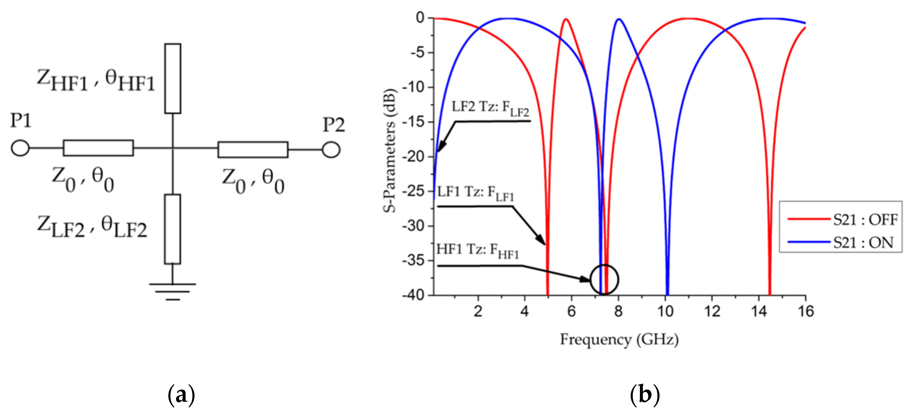
DBRs are based on the parallel association of two bandstop structures that can be two open-ended stubs, a quarter wavelength long, at a specific frequency (Figure 1a). Each resonator has its own specific length to give a transmission zero. By appropriately selecting these transmission zeroes (TZ), a bandpass filter can be obtained.
Thus, the longer resonator in Figure 1a is for the low-frequency (LF1) transmission zero and the shorter one is for the high-frequency (HF1) transmission zero. Figure 1b shows an example of simplified simulated results, i.e., without end effects or dielectric losses, obtained using the Advanced Design Systems (ADS) electronics software from Keysight Technologies©, where the two TZ make a 5.7 GHz bandpass filter possible. Then, if one resonator is short-circuited, this modifies the transmission zero and, consequently, the central frequency of the bandpass filter.
By using one active element, there are two alternative ways to create a switchable DBR. The first option is to short-circuit a stub as shown in Figure 2a; the LF transmission zero LF1 becomes LF2, thus modifying the central frequency from 5.7 GHz to 3.2 GHz (Figure 2b) in the OFF and ON states, respectively. The second option is to short-circuit the high-frequency resonator (Figure 3a); the high-frequency transmission zero HF1 becomes HF2, which makes it possible to switch the central frequency from 5.7 GHz in the OFF state to 2.5 GHz in the ON state (Figure 3b).

3. Switchable DBR Demonstrator

Based on the switchable DBR concept, our objective here was to co-design a DBR and its active element on a high-resistivity silicon (HR-Si) substrate. Indeed, a high resistivity was chosen to minimize the losses of the propagating waves in the substrate. Furthermore, the advantage of using this kind of substrate, i.e., a semiconductor, is that it makes it possible to design transmission lines and ScDDAs at the same time and thus to co-design a switchable DBR. We can, therefore, optimize electrical performances of the two states and enhance the integrability by using a low-cost technology compatible with mass-production.

3.1. Design and Modeling

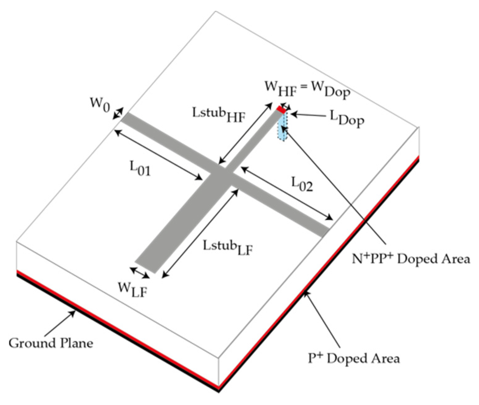
A P-type silicon substrate was chosen with a 675 µm thickness and doped with boron with a resistivity of 2500 Ω·cm. The active element was an N+PP+ junction with a surface doping of around 3 × 10¹⁹ atoms/cm3 for the two N+ and P+ regions and doping depths of around 3 µm. Figure 4 shows the switchable DBR design with its integrated active element, located at the end of the HF resonator. The length × width dimensions of the low- and high-frequency stubs are noted LstubHF × WHF and LstubLF × WLF, respectively, and the dimensions of the doped area are noted LDOP × WDOP. The lengths and widths of the two resonators were calculated to obtain a low-frequency transmission zero at 4.8 GHz and a high-frequency transmission zero at 7.2 GHz, based on the synthesis in [17]. The access line widths were dimensioned to have a 50 Ω characteristic impedance and their lengths were chosen to be sufficiently long to be easily measured. The DBR dimensions are listed in Table 1.
This demonstrator was simulated using an HFSSTM electromagnetic simulator to predict its behavior. The semiconductor losses were taken into account using the substrate resistivity in the calculation loss tangent as follows:
t a n δ = 1 ρ ω ε 0 ε r + 0.0018
where ρ is the resistivity, ω is equal to 2 π f r e q , ε 0 is the vacuum dielectric permittivity and ε r is the silicon dielectric permittivity, equal to 11.9.
The active element was simulated using two 3 µm deep layers of 7.1 × 10⁵ S/m conductivity, corresponding to the conductivity of heavily doped areas. Between these two layers, i.e., between the top and the bottom sides, within the substrate itself, a resistivity of 2500 Ω·cm in the OFF state and a resistivity of 0.1 Ω·cm in the ON state, which was estimated using AtlasTM from Silvaco© when the junction was forward biased. Figure 5 presents the electromagnetic simulated results of the switchable DBR1 demonstrator in OFF and ON states. In the OFF state, the two transmission zeroes at 4.8 GHz and 7.2 GHz make it possible to obtain a bandpass filter at 5.52 GHz. When the N+PP+ is simulated in forward bias, the high-frequency transmission zero is switched to DC allowing a transmission frequency band at 2.44 GHz. The simulated insertion losses are 0.9 dB at 5.52 GHz in the OFF state and 2.01 dB at 2.44 GHz in the ON state.

3.2. Fabrication and Measurements

This demonstrator was fabricated with only two masks: one for the doping steps and one for the metallization steps of the upper side. The manufacturing steps are detailed in [27].
Figure 6 shows a photograph of the switchable DBR1 demonstrator, placed between two SMA connectors for measurement. The two RF cables and DC source were connected to an R&S® ZVA 67 Vector Network Analyzer (VNA). The DC bias voltage was applied with the RF signal. Because the DC ground was connected to the RF ground, a negative voltage was required to forward bias the N+PP+ junction. A Short Open Load through (SOLT) calibration was performed to remove the losses of the cables but not the losses from the SMA connectors.
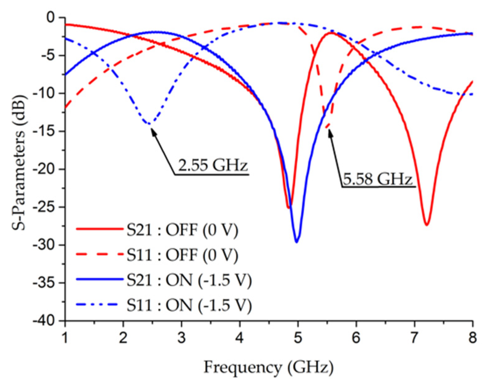
The measured results are presented in Figure 7. In the OFF state, with a zero-bias voltage, the two transmission zeroes are measured at 4.83 GHz and 7.2 GHz, which implies a central frequency at 5.58 GHz with an insertion loss level of 1.97 dB. In the ON state, the lowest frequency transmission zero stays relatively constant, whereas the high-frequency transmission zero is moved to the DC frequency so the central frequency is switched to 2.55 GHz with a bias voltage of −1.5 V. The insertion loss level is then 1.9 dB.
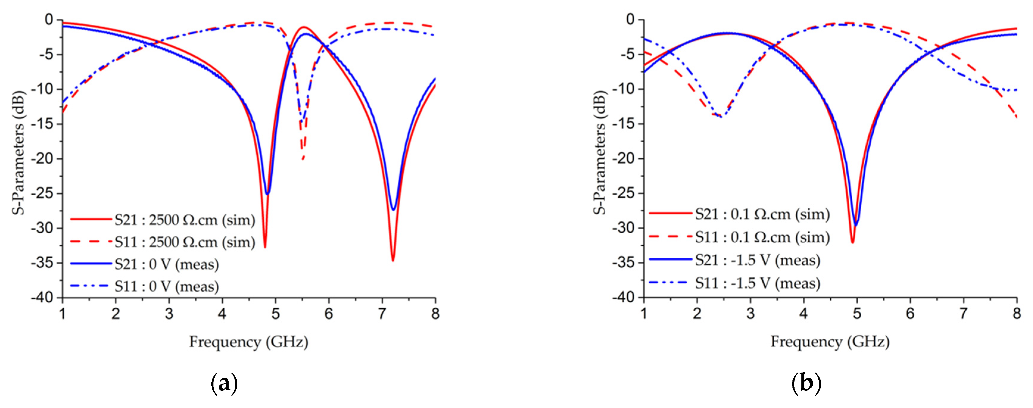
Figure 8a,b show comparisons of the simulated and measured results in the OFF and ON states. A good agreement was obtained overall, with slight differences that could be due to the substrate resistivity (given by the manufacturer as between 1 kΩ·cm and 10 kΩ·cm), the SMA connector losses themselves and the losses related to connection defects, i.e., the gap that exists between the connector and the substrate because these are separate elements.

4. Discussion

The co-design approach used in the present study offers great flexibility and accuracy for the dimensioning and positioning of the doped areas, thanks to the semiconductor process. In order to show an overview of the possibilities, three other demonstrators (Figure 9) with different doped lengths and widths were designed and characterized. These switchable DBRs had the same metal layout as the first demonstrator DBR1, only the dimensions (listed in Table 2) of the doped areas (located at the end of the resonator) were modified.
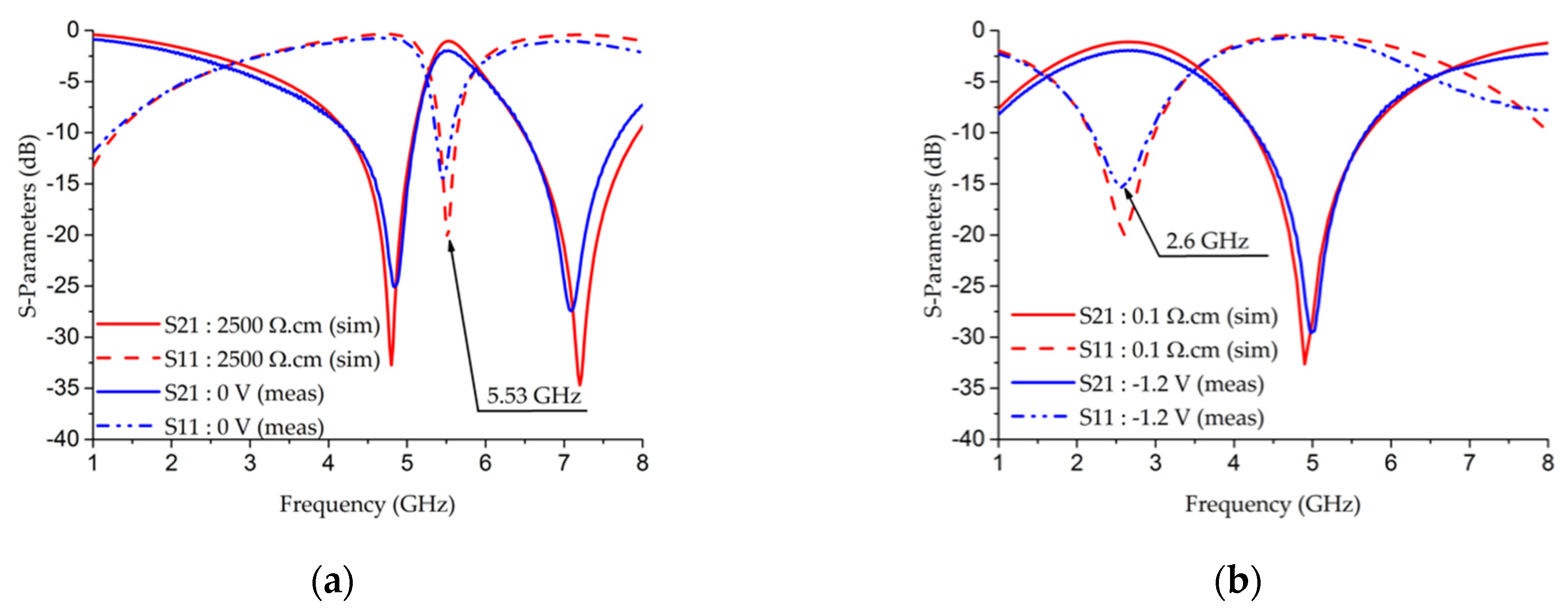
Figure 10a,b show comparisons of the simulated and measured results of switchable DBR2 in the OFF and ON states. As for DBR1, a good agreement was obtained overall. It has a longer ScDDA than DBR1 on the HF stub, with 1 mm length. Therefore, compared with DBR1, the central frequency is the same in the OFF state, i.e., equal to 5.53 GHz, with a 0 V bias voltage. The insertion loss level is 1.97 dB. In the ON state, with a −1.2 V bias voltage, the highest transmission zero is moved to DC and the transmission frequency band is at 2.6 GHz, with an insertion loss level of 1.95 dB. The bias voltage is lower than for DBR1 because the doped area is longer.
Switchable DBR3 has an ScDDA with a doped length of 0.2 mm, located at the end of the LF resonator. Figure 11a,b show comparisons of the simulated and measured results of switchable DBR3 in the OFF and ON states. These figures show a commutation in the central frequency from 5.53 GHz in the OFF state, with a 0 V bias voltage, to 3.23 GHz in the ON state, with a −1.5 V bias voltage. The insertion loss levels are 1.98 dB and 1.68 dB, respectively.
The last demonstrator, DBR4, has a wider and longer ScDDA than DBR3. This implies a capacitive effect in the OFF state, which explains why the resonant frequency, at 5.2 GHz, is lower than for the other demonstrators (Figure 12a). It also has a shorter resonator in the ON state, which gives a resonant frequency of 3.8 GHz in the ON state (higher than with DBR3) (Figure 12b), with a bias voltage of −1 V. The insertion losses are 1.94 dB and 1.95 dB in the OFF and ON states, respectively.
Moreover, with a 5.52 GHz filter in the OFF state, the central frequency in the ON state can be selected between 2.44 GHz and 5 GHz by choosing the length of the doped area and short-circuiting the LF- or HF- stub (Figure 13). The ratio can be between 1:1.1 and 1:2.25, which offers many possibilities depending on the application. The greater the doped area surface, the lower the bias voltage. Thus, if the bias voltage is not an issue, the size can be minimized while maintaining the switched frequency. This can be a good solution in the case of multiple states, such as in [25].
Table 3 shows a comparison between the state-of-the-art and the results of the present study. Our work shows a great agility, with the best tradeoff between the highest frequency ratio and good performances, i.e., low losses, without any additional components.
Although devices of this kind present measurement difficulties due to their fragility and size and, therefore, require measurement by SMA connectors without the possibility of soldering, the devices tested here show good performances in both states, with the same losses overall. Indeed, in the ON state, even though the demonstrators have different surface areas, their equivalent resistance values can be roughly the same with different bias voltages.

5. Conclusions

This paper shows a novel method for switching DBR filters without any additional components. Four demonstrators were characterized, offering a large range of reconfigurability without sacrificing performances, i.e., a low switching voltage, low losses, and a high level of integrability, all obtained with a well-known manufacturing process (the same as for semiconductor components), with a reduced number of masks and steps. Such a co-design offers flexibility in terms of positioning and dimensioning of the ScDDAs, which implies a good agility, with a large range of choice for the ratio: between 1:1.1 and 1:2.25.

Author Contributions

Investigation, R.A.; Resources, R.A., D.L.B., C.Q., D.C., V.G., D.V. and J.B.; Writing—original draft, R.A. All authors have read and agreed to the published version of the manuscript.

Funding

This research received no external funding.

Acknowledgments

The authors would like to thank the TECHYP platform (the High Performance Computing Cluster at Lab-STICC) thanks to which the devices could be simulated. This work was partly supported by the French CERTeM Technological Platform and by the French RENATECH network. This publication is supported by the European Union through the European Regional Development Fund (ERDF), by the Ministry of Higher Education and Research and Brittany Brest Métropole, through the CPER Project SOPHIE/STIC & Ondes.

Conflicts of Interest

The authors declare no conflict of interest.

References

  1. Kumar, N.; Singh, Y.K. RF-MEMS-based bandpass-to-bandstop switchable single- and dual-band filters with variable FBW and reconfigurable selectivity. IEEE Trans. Microw. Theory Tech. 2017, 65, 3824–3837. [Google Scholar] [CrossRef]
  2. Fan, M.; Song, K.; Zhu, Y.; Fan, Y. Compact Bandpass-to-Bandstop Reconfigurable Filter with Wide Tuning Range. IEEE Microw. Wirel. Compon. Lett. 2019, 29, 198–200. [Google Scholar] [CrossRef]
  3. Yang, T.; Rebeiz, G.M. A 1.9–2.6 GHz filter with both bandpass-to-bandstop reconfigurable function and bandpass-and-bandstop cascading function. In Proceedings of the 2017 IEEE MTT-S International Microwave Symposium (IMS), Honololu, HI, USA, 4–9 June 2017; pp. 264–266. [Google Scholar]
  4. Naglich, E.J.; Lee, J.; Peroulis, D.; Chappell, W.J. A tunable bandpass-to-bandstop reconfigurable filter with independent bandwidths and tunable response shape. IEEE Trans. Microw. Theory Tech. 2010, 58, 3770–3779. [Google Scholar] [CrossRef]
  5. Cheng, T.; Tam, K.-W. A wideband bandpass filter with reconfigurable bandwidth based on cross-shaped resonator. IEEE Microw. Wirel. Compon. Lett. 2017, 27, 909–911. [Google Scholar] [CrossRef]
  6. Tu, W.-H. Compact Low-Loss Reconfigurable Bandpass Filter with Switchable Bandwidth. IEEE Microw. Wirel. Compon. Lett. 2010, 20, 208–210. [Google Scholar] [CrossRef]
  7. Lugo, C.; Papapolymerou, J. Electronic switchable bandpass filter using PIN diodes for wireless low cost system-on-a-package applications. IEEE Proc. Microw. Antennas Propag. 2004, 151, 497–502. [Google Scholar] [CrossRef]
  8. Brito-Brito, Z.; Llamas-Garro, I.; Navarro-Munoz, G.; Perruisseau-Carrier, J.; Pradell, L. UMTS-WiFi switchable bandpass filter. In Proceedings of the 2009 European Microwave Conference (EuMC), Rome, Italy, 29 September–1 October 2009; pp. 125–128. [Google Scholar]
  9. Wong, P.W.; Hunter, I. A New Class of Low-Loss High-Linearity Electronically Reconfigurable Microwave Filter. IEEE Trans. Microw. Theory Tech. 2008, 56, 1945–1953. [Google Scholar] [CrossRef]
  10. Mahe, F.; Tanne, G.; Rius, E.; Person, C.; Toutain, S.; Biron, F.; Billonnet, L.; Jarry, B.; Guillon, P. Electronically Switchable Dual-Band Microstrip Interdigital Bandpass Filter For Multistandard Communication Applications. In Proceedings of the 2000 30th European Microwave Conference, Paris, France, 2–5 October 2000. [Google Scholar]
  11. Chen, C.-C.; Wang, S.-M. Design of an LTCC switchable filter for Dual-Band RF Front-End applications. In Proceedings of the TENCON 2007—2007 IEEE Region 10 Conference, Taipei, Taiwan, 30 October–2 November 2007. [Google Scholar]
  12. Weng, S.; Hsu, K.; Tu, W. Switchable and High-Isolation Diplexer with Wide Stopband. IEEE Microw. Wirel. Compon. Lett. 2014, 24, 373–375. [Google Scholar] [CrossRef]
  13. Xu, J. Compact Switchable Bandpass Filter and Its Application to Switchable Diplexer Design. IEEE Microw. Wirel. Compon. Lett. 2016, 26, 13–15. [Google Scholar] [CrossRef]
  14. Yang, S.; Li, W.; Vaseem, M.; Shamim, A. Fully Printed VO2 Switch Based Flexible and Reconfigurable Filter. In Proceedings of the 2020 IEEE/MTT-S International Microwave Symposium (IMS), Los Angeles, CA, USA, 4–6 August 2020; pp. 49–52. [Google Scholar] [CrossRef]
  15. Ninic, M.; Jokanovic, B.; Meyer, P. Reconfigurable Multi-State Composite Split-Ring Resonators. IEEE Microw. Wirel. Compon. Lett. 2016, 26, 267–269. [Google Scholar] [CrossRef]
  16. Lugo, C.; Papapolymerou, J. Six-State Reconfigurable Filter Structure for Antenna Based Systems. IEEE Trans. Antennas Propag. 2006, 54, 479–483. [Google Scholar] [CrossRef]
  17. Quendo, C.; Rius, E.; Person, C. Narrow bandpass filters using dual-behavior resonators based on stepped-impedance stubs and different-length stubs. IEEE Trans. Microw. Theory Tech. 2004, 52, 1034–1044. [Google Scholar] [CrossRef]
  18. Quendo, C.; Rius, E.; Person, C. An original topology of dual-band filter with transmission zeros. In Proceedings of the IEEE MTT-S International Microwave Symposium Digest, 2003, Philadelphia, PA, USA, 8–13 June 2003; Volume 2, pp. 1093–1096. [Google Scholar]
  19. Foum, E.; Rius, E.; Tanne, G.; Manchec, A.; Quendo, C. Frequency Variations Improvement of a Bandwidth and Central Frequency Reconfigurable DBR Filter. In Proceedings of the 2006 European Microwave Conference, Manchester, UK, 10–15 September 2006. [Google Scholar]
  20. Gómez-García, R.; Muñoz-Ferreras, J.-M.; Psychogiou, D. Dual-Behavior Resonator-Based Fully Reconfigurable Input Reflectionless Bandpass Filters. IEEE Microw. Wirel. Compon. Lett. 2019, 29, 35–37. [Google Scholar] [CrossRef]
  21. Othman, A.; Barrak, R.; Mabrouk, M. New approach to design tunable RF filters using DBR topology for SDR receivers. In Proceedings of the 2013 13th Mediterranean Microwave Symposium (MMS), Saida, Lebanon, 2–5 September 2013; pp. 1–4. [Google Scholar]
  22. Laur, V.; Moussavou, A.; Tanne, G.; Laurent, P.; Bouquet, V.; Deputier, S.; Guilloux-Viry, M.; Huret, F. Tunable DBR resonators using KTN ferroelectric thin-films. In Proceedings of the 2007 IEEE/MTT-S International Microwave Symposiumpp, Honolulu, HI, USA, 3–8 June 2007; pp. 2059–2062. [Google Scholar]
  23. Allanic, R.; Quéré, Y.; le Berre, D.; Quendo, C. A Novel Approach to Co-Design microwave Devices with Distributed Switches. In Proceedings of the 2016 Asia-Pacific Microwave Conference (APMC), New Delhi, India, 5–9 December 2016. [Google Scholar]
  24. Allanic, R.; Quéré, Y.; le Berre, D.; Quendo, C. Intrinsically microwave tunable resonator designed on silicon. IEEE Electron. Lett. 2016, 52, 1697–1699. [Google Scholar] [CrossRef]
  25. Allanic, R.; le Berre, D.; Quere, Y.; Quendo, C.; Chouteau, D.; Grimal, V.; Valente, D.; Billoue, J. Three-State Microwave Tunable Resonator Integrating Several Active Elements on Silicon Technology in a Global Design. IEEE Microw. Wirel. Compon. Lett. 2018, 28, 141–143. [Google Scholar] [CrossRef]
  26. Allanic, R.; le Berre, D.; Quere, Y.; Quendo, C.; Chouteau, D.; Grimal, V.; Valente, D.; Billoue, J. Continuously Tunable Resonator Using a Novel Triangular Doped Area on a Silicon Substrate. IEEE Microw. Wirel. Compon. Lett. 2018, 28, 1095–1097. [Google Scholar] [CrossRef]
  27. Allanic, R.; le Berre, D.; Quere, Y.; Quendo, C.; Chouteau, D.; Grimal, V.; Valente, D.; Billoue, J. A Novel Synthesis for Bandwidth Switchable Bandpass Filters Using Semi-conductor Distributed Doped Areas. IEEE Access 2020, 8, 122599–122609. [Google Scholar] [CrossRef]
Figure 1. (a) Dual behavior resonator (DBR) design in the OFF state with two open-ended stubs linked to the two frequencies LF1 and HF1; (b) example of simulated results with the two transmission zeroes for a central frequency of 5.6 GHz.
Electronics 09 02021 g001
Figure 2. (a) DBR design in the ON state with the LF2 stub short-circuited and the HF1 stub open-circuited; (b) Example of simulated results for central frequencies of 5.7 GHz in the OFF state and 3.2 GHz in the ON state.
Electronics 09 02021 g002
Figure 3. (a) DBR design in the ON state with the LF1 stub open-circuited and the HF2 stub short-circuited; (b) Example of simulated results for central frequencies of 5.7 GHz in the OFF state and 2.5 GHz in the ON state.
Electronics 09 02021 g003
Figure 4. 3-D diagram of the switchable DBR1 demonstrator.
Electronics 09 02021 g004
Figure 5. HFSSTM-simulated results of switchable DBR1 in the OFF and ON states.
Electronics 09 02021 g005
Figure 6. Photograph of switchable DBR1.
Electronics 09 02021 g006
Figure 7. Measured results of switchable DBR1 in the OFF and ON states.
Electronics 09 02021 g007
Figure 8. Comparison of simulated and measured results of switchable DBR1. (a) in the OFF state; (b) in the ON state.
Electronics 09 02021 g008
Figure 9. Top views of switchable DBRs. (a) DBR1 with doped area dimensions of 0.2 mm × 0.314 mm. (b) DBR2 with doped area dimensions of 1 mm × 0.314 mm. (c) DBR3 with doped area dimensions of 0.2 mm × 0.836 mm. (d) DBR4 with doped area dimensions of 2 mm × 1.5 mm. Measured results of switchable DBR1 in the OFF and ON states.
Electronics 09 02021 g009
Figure 10. Comparison of simulated and measured results of switchable DBR2. (a) in the OFF state; (b) in the ON state.
Electronics 09 02021 g010
Figure 11. Comparison of simulated and measured results of switchable DBR3. (a) in the OFF state; (b) in the ON state.
Electronics 09 02021 g011
Figure 12. Comparison of simulated and measured results of switchable DBR4. (a) in the OFF state; (b) in the ON state.
Electronics 09 02021 g012
Figure 13. Central frequency of a switchable DBR in the ON state depending on the doped area length, for a central frequency of 5.52 GHz in the OFF state.
Electronics 09 02021 g013
Table 1. Dimensions of Switchable DBR1.
AccessLF ResonatorHF ResonatorScDDAs
LengthL01 = 3.74 mm
L02 = 4 mm
LstubLF = 5.46 mmLstubHF = 3.8 mmLDop = 0.2 mm
WidthW0 = 0.56 mmWstubLF = 0.84 mmWstubHF = 0.31 mmWDop = 0.31 mm
Table 2. Dimensions of the ScDDAs of the four demonstrators.
ScDDA of DBR1ScDDA of DBR2ScDDA of DBR3ScDDA of DBR4
LengthLDop = 0.2 mmLDop = 1 mmLDop = 0.2 mmLDop = 2 mm
WidthWDop = 0.31 mmWDop = 0.31 mmWDop = 0.84 mmWDop = 1.5 mm
Table 3. Comparison between previous two-state switchable filters and this work.
Ref.Freq. (GHz)
LF Band
Freq. (GHz)
HF Band
IL (dB)
LF Band
IL (dB)
HF Band
Active ComponentsFrequency Ratio
[8]1.942.433.843.35PIN diodes1:1.25
[9]1.061.511.71.7PIN diodes1:1.42
[10]1.922.083.943.07PIN diodes1:1.08
[10]2.034.4724.463.77PIN diodes1:2.2
[11]2.534.93.772.64PIN diodes1:1.94
[12]1.21.52.12.21PIN diodes1:1.25
[13]0.901.251.81.9PIN diodes1:1.38
[14]3.742.62.6Vanadium-di-oxide1:1.08
This study DBR12.555.581.971.9Integrated ScDDA1:2.19
This study
DBR2
2.65.531.971.95Integrated ScDDA1:2.13
This study
DBR3
3.235.531.981.68Integrated ScDDA1:1.71
This study
DBR4
3.85.21.941.95Integrated ScDDA1:1.37
Publisher’s Note: MDPI stays neutral with regard to jurisdictional claims in published maps and institutional affiliations.